

Page 1
1-385
H
High Bandwidth, Analog/Video
Optocouplers
Technical Data
Features
• Wide Bandwidth
[1]
:
17 MHz (HCPL-4562)
9 MHz (HCNW4562)
• High Voltage Gain
[1]
:
2.0 (HCPL-4562)
3.0 (HCNW4562)
• Low GV Temperature
Coefficient: -0.3%/°C
• Highly Linear at Low Drive
Currents
• High-Speed AlGaAs Emitter
• Safety Approval
UL Recognized - 2500 V rms
for 1 minute (5000 V rms for
1 minute for HCPL4562#020 and HCNW4562)
per UL 1577
CSA Approved
VDE 0884 Approved
-V
IORM
= 1414 V peak for
HCNW4562
BSI Certified (HCNW4562)
• Available in 8-Pin DIP and
Widebody Packages
Applications
• Video Isolation for the
Following Standards/
Formats: NTSC, PAL,
SECAM, S-VHS, ANALOG
RGB
• Low Drive Current Feedback
Element in Switching Power
Supplies, e.g., for ISDN
Networks
• A/D Converter Signal
Isolation
• Analog Signal Ground
Isolation
• High Voltage Insulation
Description
The HCPL-4562 and HCNW4562
optocouplers provide wide bandwidth isolation for analog signals.
They are ideal for video isolation
when combined with their
application circuit (Figure 4).
High linearity and low phase shift
are achieved through an AlGaAs
LED combined with a high speed
detector. These single channel
optocouplers are available in
8-Pin DIP and Widebody package
configurations.
HCPL-4562
HCNW4562
CAUTION: It is advised that normal static precautions be taken in handling and assembly of this component to
prevent damage and/or degradation which may be induced by ESD.
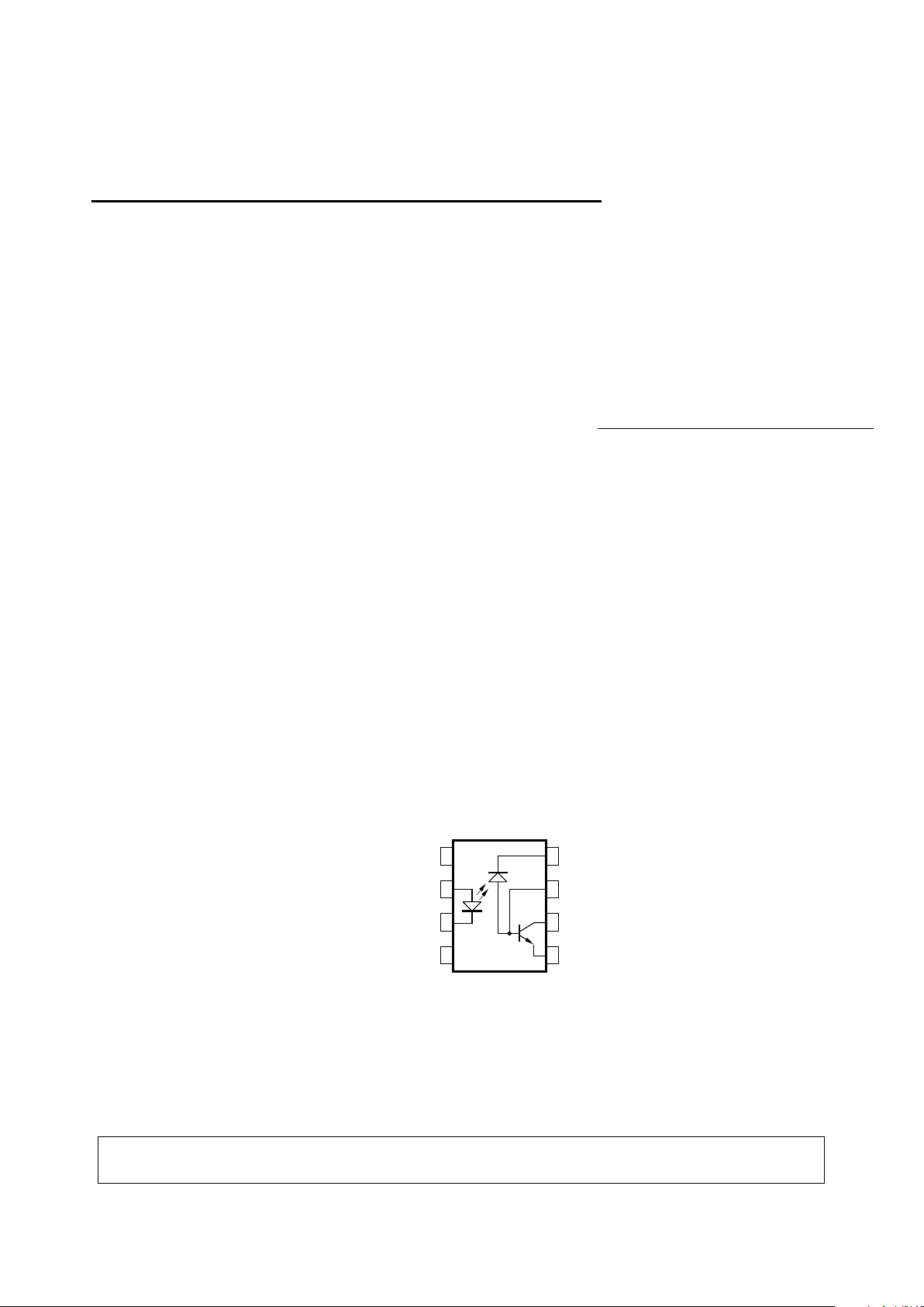
Functional Diagram
7
1
2
3
4
5
6
8
NC
ANODE
CATHODE
NC
V
CC
V
B
V
O
GND
5965-3579E
Page 2
1-386
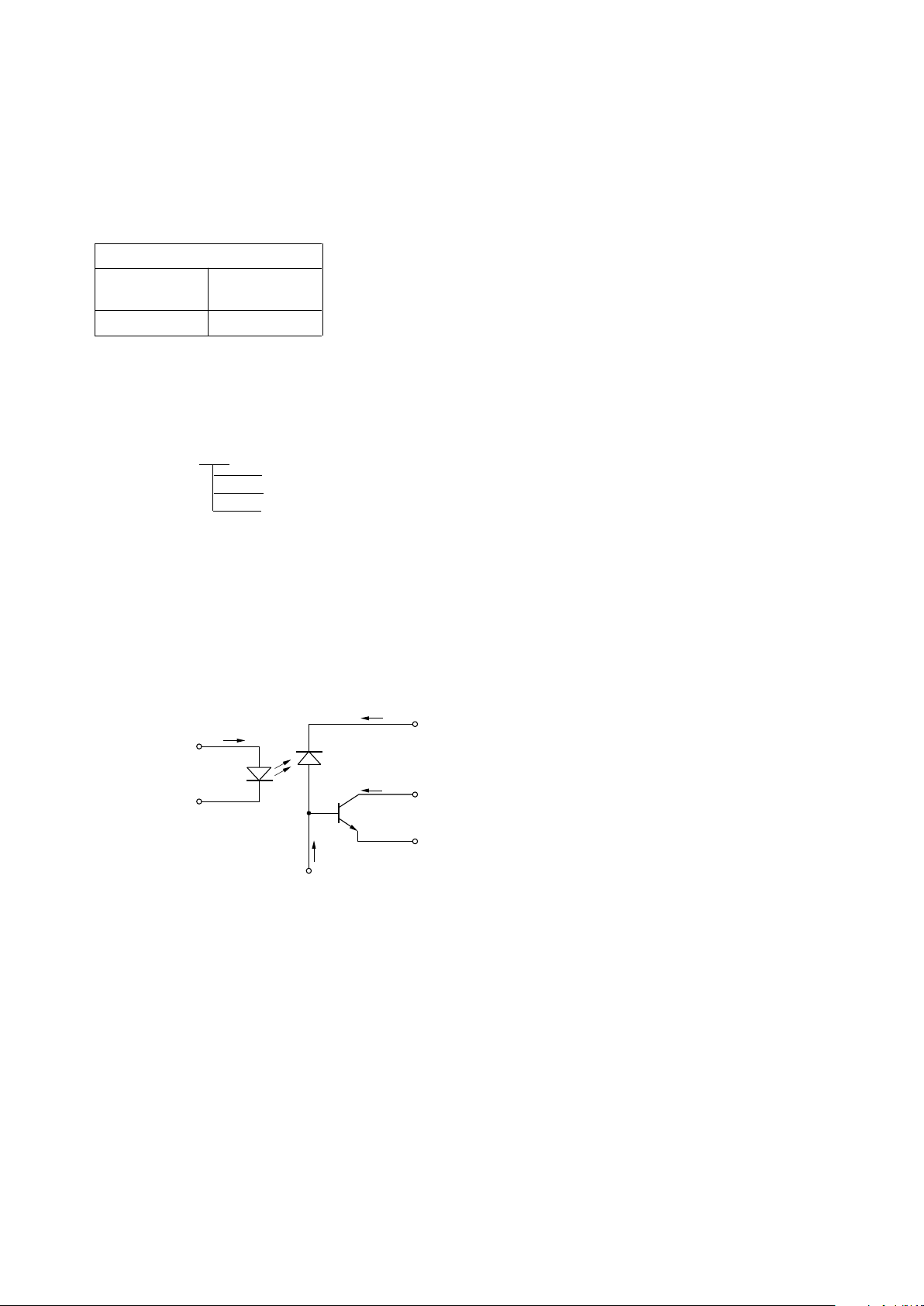
Selection Guide
Single Channel Packages
8-Pin DIP Widebody
(300 Mil) (400 Mil)
HCPL-4562 HCNW4562
Ordering Information
Specify Part Number followed by Option Number (if desired).
Example:
HCPL-4562#XXX
020 = UL 5000 V rms/1 Minute Option*
300 = Gull Wing Surface Mount Option†
500 = Tape and Reel Packaging Option
Option data sheets are available. Contact your Hewlett-Packard sales representative or authorized
distributor for information.
*For HCPL-4562 only.
†Gull wing surface mount option applies to through hole parts only.
Schematic
I
F
8
6
5
GND
V
CC
2
3
V
O
I
CC
V
F
I
O
ANODE
CATHODE
+
–
7
V
B
I
B
Page 3
1-387
Package Outline Drawings
8-Pin DIP Package (HCPL-4562)
8-Pin DIP Package with Gull Wing Surface Mount Option 300 (HCPL-4562)
0.635 ± 0.25
(0.025 ± 0.010)
12° NOM.
9.65 ± 0.25
(0.380 ± 0.010)
0.635 ± 0.130
(0.025 ± 0.005)
7.62 ± 0.25
(0.300 ± 0.010)
5
6
7
8
4
3
2
1
9.65 ± 0.25
(0.380 ± 0.010)
6.350 ± 0.25
(0.250 ± 0.010)
1.016 (0.040)
1.194 (0.047)
1.194 (0.047)
1.778 (0.070)
9.398 (0.370)
9.906 (0.390)
4.826
(0.190)
TYP.
0.381 (0.015)
0.635 (0.025)
PAD LOCATION (FOR REFERENCE ONLY)
1.080 ± 0.320
(0.043 ± 0.013)
4.19
(0.165)
MAX.
1.780
(0.070)
MAX.
1.19
(0.047)
MAX.
2.54
(0.100)
BSC
DIMENSIONS IN MILLIMETERS (INCHES).
LEAD COPLANARITY = 0.10 mm (0.004 INCHES).
0.254
+ 0.076
- 0.051
(0.010
+ 0.003)
- 0.002)
9.65 ± 0.25
(0.380 ± 0.010)
1.78 (0.070) MAX.
1.19 (0.047) MAX.
HP XXXXZ
YYWW
DATE CODE
1.080 ± 0.320
(0.043 ± 0.013)
2.54 ± 0.25
(0.100 ± 0.010)
0.51 (0.020) MIN.
0.65 (0.025) MAX.
4.70 (0.185) MAX.
2.92 (0.115) MIN.
DIMENSIONS IN MILLIMETERS AND (INCHES).
5678
4321
5° TYP.
OPTION NUMBER*
UL
RECOGNITION
UR
0.254
+ 0.076
- 0.051
(0.010
+ 0.003)
- 0.002)
7.62 ± 0.25
(0.300 ± 0.010)
6.35 ± 0.25
(0.250 ± 0.010)
* MARKING CODE LETTER FOR OPTION NUMBERS.
"L" = OPTION 020
"V" = OPTION 060
OPTION NUMBERS 300 AND 500 NOT MARKED.
TYPE NUMBER
Page 4
1-388
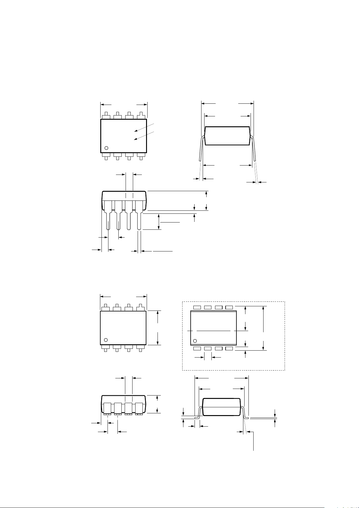
8-Pin Widebody DIP Package (HCNW4562)
8-Pin Widebody DIP Package with Gull Wing Surface Mount Option 300 (HCNW4562)
5
6
7
8
4
3
2
1
11.15 ± 0.15
(0.442 ± 0.006)
1.78 ± 0.15
(0.070 ± 0.006)
5.10
(0.201)
MAX.
1.55
(0.061)
MAX.
2.54 (0.100)
TYP.
DIMENSIONS IN MILLIMETERS (INCHES).
7° TYP.
0.254
+ 0.076
- 0.0051
(0.010
+ 0.003)
- 0.002)
11.00
(0.433)
9.00 ± 0.15
(0.354 ± 0.006)
MAX.
10.16 (0.400)
TYP.
HP
HCNWXXXX
YYWW
DATE CODE
TYPE NUMBER
0.51 (0.021) MIN.
0.40 (0.016)
0.56 (0.022)
3.10 (0.122)
3.90 (0.154)
1.00 ± 0.15
(0.039 ± 0.006)
7° NOM.
12.30 ± 0.30
(0.484 ± 0.012)
0.75 ± 0.25
(0.030 ± 0.010)
11.00
(0.433)
5
6
7
8
4
3
2
1
11.15 ± 0.15
(0.442 ± 0.006)
9.00 ± 0.15
(0.354 ± 0.006)
1.3
(0.051)
12.30 ± 0.30
(0.484 ± 0.012)
6.15
(0.242)
TYP.
0.9
(0.035)
PAD LOCATION (FOR REFERENCE ONLY)
1.78 ± 0.15
(0.070 ± 0.006)
4.00
(0.158)
MAX.
1.55
(0.061)
MAX.
2.54
(0.100)
BSC
DIMENSIONS IN MILLIMETERS (INCHES).
LEAD COPLANARITY = 0.10 mm (0.004 INCHES).
0.254
+ 0.076
- 0.0051
(0.010
+ 0.003)
- 0.002)
MAX.
Page 5
1-389
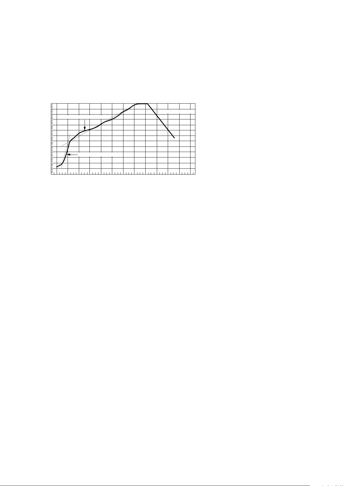
Note: Use of nonchlorine activated fluxes is highly recommended.
240
∆T = 115°C, 0.3°C/SEC
0
∆T = 100°C, 1.5°C/SEC
∆T = 145°C, 1°C/SEC
TIME – MINUTES
TEMPERATURE – °C
220
200
180
160
140
120
100
80
60
40
20
0
260
123456789101112
Solder Reflow Temperature Profile (Gull Wing Surface Mount Option Parts)
Regulatory Information
The devices contained in this data
sheet have been approved by the
following organizations:
UL
Recognized under UL 1577,
Component Recognition
Program, File E55361.
CSA
Approved under CSA Component
Acceptance Notice #5, File CA
88324.
VDE
Approved according to VDE
0884/06.92 (HCNW4562 only).
BSI
Certification according to
BS415:1994
(BS EN60065:1994);
BS EN60950:1992
(BS7002:1992) and
EN41003:1993 for Class II
applications (HCNW4562 only).
Page 6

1-390
Insulation and Safety Related Specifications
8-Pin DIP Widebody
(300 Mil) (400 Mil)
Parameter Symbol Value Value Units Conditions
Minimum External L(101) 7.1 9.6 mm Measured from input terminals to
Air Gap (External output terminals, shortest distance
Clearance) through air.
Minimum External L(102) 7.4 10.0 mm Measured from input terminals to
Tracking (External output terminals, shortest distance
Creepage) path along body.
Minimum Internal 0.08 1.0 mm Through insulation distance,
Plastic Gap conductor to conductor, usually the
(Internal Clearance) direct distance between the photo-
emitter and photodetector inside the
optocoupler cavity.
Minimum Internal NA 4.0 mm Measured from input terminals to
Tracking (Internal output terminals, along internal cavity.
Creepage)
Tracking Resistance CTI 200 200 Volts DIN IEC 112/VDE 0303 Part 1
(Comparative
Tracking Index)
Isolation Group IIIa IIIa Material Group
(DIN VDE 0110, 1/89, Table 1)
Option 300 - surface mount classification is Class A in accordance with CECC 00802.
Page 7

1-391
VDE 0884 Insulation Related Characteristics (HCNW4562 ONLY)
Description Symbol Characteristic Units
Installation classification per DIN VDE 0110/1.89, Table 1
for rated mains voltage ≤ 600 V rms I-IV
for rated mains voltage ≤ 1000 V rms I-III
Climatic Classification 55/85/21
Pollution Degree (DIN VDE 0110/1.89) 2
Maximum Working Insulation Voltage V
IORM
1414 V peak
Input to Output Test Voltage, Method b*
V
IORM
x 1.875 = VPR, 100% Production Test with tm = 1 sec, V
PR
2652 V peak
Partial Discharge < 5 pC
Input to Output Test Voltage, Method a*
V
IORM
x 1.5 = VPR, Type and sample test, V
PR
2121 V peak
tm = 60 sec, Partial Discharge < 5 pC
Highest Allowable Overvoltage*
(Transient Overvoltage, t
ini
= 10 sec) V
IOTM
8000 V peak
Safety Limiting Values
(Maximum values allowed in the event of a failure,
also see Figure 17, Thermal Derating curve.)
Case Temperature T
S
150 °C
Input Current I
S,INPUT
400 mA
Output Power P
S,OUTPUT
700 mW
Insulation Resistance at TS, VIO = 500 V R
S
≥ 10
9
Ω
*Refer to the front of the optocoupler section of the current catalog, under Product Safety Regulations section (VDE 0884), for a
detailed description.
Note: Isolation characteristics are guaranteed only within the safety maximum ratings which must be ensured by protective circuits in
application.
Page 8

1-392
Absolute Maximum Ratings
Parameter Symbol Device Min. Max. Units Note
Storage Temperature T
S
-55 125 °C
Operating Temperature T
A
-40 85 °C
Average Forward Input Current I
F(avg)
HCPL-4562 12 mA
HCNW4562 25
Peak Forward Input Current I
F(PEAK)
HCPL-4562 18.6 mA
HCNW4562 40
Effective Input Current I
F(EFF)
HCPL-4562 12.9 mA rms
Reverse LED Input Voltage (Pin 3-2) V
R
HCPL-4562 1.8 V
HCNW4562 3
Input Power Dissipation P
IN
HCNW4562 40 mW
Average Output Current (Pin 6) I
O(AVG)
8mA
Peak Output Current (Pin 6) I
O(PEAK)
16 mA
Emitter-Base Reverse Voltage (Pin 5-7) V
EBR
5V
Supply Voltage (Pin 8-5) V
CC
-0.3 30 V
Output Voltage (Pin 6-5) V
O
-0.3 20 V
Base Current (Pin 7) I
B
5mA
Output Power Dissipation P
O
100 mW 2
Lead Solder Temperature T
LS
HCPL-4562 260 °C
HCNW4562 260 °C
Reflow Temperature Profile T
RP
Option
300 Drawings Section
1.6 mm Below Seating Plane, 10 Seconds
up to Seating Plane, 10 Seconds
Recommended Operating Conditions
Parameter Symbol Device Min. Max. Units Note
Operating Temperature T
A
HCPL-4562 -10 70 °C
Quiescent Input Current I
FQ
HCPL-4562 6 mA
HCNW4562 10
Peak Input Current I
F(PEAK)
HCPL-4562 10 mA
HCNW4562 17
See Package Outline
Page 9

1-393
Electrical Specifications (DC)
TA = 25°C, IF = 6 mA for HCPL-4562 and IF = 10 mA for HCNW4562 (i.e., Recommended IFQ) unless
otherwise specified.
Parameter Symbol Device Min. Typ.* Max. Units Test Conditions Fig. Note
Base Photo I
PB
13 31 65 µAIF = 10 mA VPB ≥ 5 V 2, 6
Current HCPL-4562 19.2 IF = 6 mA
I
PB
∆IPB/ -0.3 %/°C 2 mA < IF < 10 mA, 2
Temperature ∆TV
PB
≥ 5 V
Coefficient
I
PB
HCPL-4562 0.25 % 2 mA < IF < 10 mA 2, 6 3
Nonlinearity HCNW4562 0.15 6 mA < IF < 14 mA
Input Forward V
F
HCPL-4562 1.1 1.3 1.6 V IF = 5 mA 5
Voltage HCNW4562 1.2 1.6 1.8 IF = 10 mA
Input Reverse BV
R
HCPL-4562 1.8 5 V IR = 10 µA
Breakdown HCNW4562 3 IR = 100 µA
Voltage
Transistor h
FE
60 160 IC = 1 mA,
Current Gain VCE = 1.25 V
Current CTR HCPL-4562 45 % VCE = 1.25 V, 8, 9 4
Transfer Ratio HCNW4562 52 VPB ≥ 5 V
DC Output V
OUT
HCPL-4562 4.25 V GV = 2, VCC = 9 V 4,
Voltage HCNW4562 5.0 15
Page 10

1-394
Small Signal Characteristics (AC)
TA = 25°C, IF = 6 mA for HCPL-4562 and IF = 10 mA for HCNW4562 (i.e., Recommended IFO) unless
otherwise specified.
Parameter Symbol Device Min. Typ.* Max. Units Test Conditions Fig. Note
Voltage Gain G
V
HCPL-4562 0.8 2.0 4.2 VIN = 1 V
P-P
16
(0.1 MHz) HCNW4562 3.0
GV Temperature ∆GV/∆T -0.3 %/°CVIN = 1 V
P-P
,1, 11
Coefficient f
REF
= 0.1 MHz
Base Photo ∆i
PB
HCPL-4562 1.1 3.0 -dB VIN = 1 V
P-P
, 3, 10,
Current (6 MHz) HCNW4562 0.36 f
REF
= 0.1 MHz 12
Variation
-3 dB Frequency i
PB
HCPL-4562 6 15 MHz VIN = 1 V
P-P
, 3, 10, 7
(i
PB
) (-3 dB) HCNW4562 13 f
REF
= 0.1 MHz 12
-3 dB Frequency G
V
HCPL-4562 6 17 MHz VIN = 1 V
P-P
, 1, 11 7
(G
V
) (-3 dB) HCNW4562 9 f
REF
= 0.1 MHz
Gain Variation ∆G
V
HCPL-4562 1.1 3.0 -dB TA = 25°CVIN = 1 V
P-P
, 1, 11
(6 MHz) HCNW4562 0.54 f
REF
= 0.1 MHz
HCPL-4562 0.8 T
A
= -10° C
1.5 T
A
= 70°C
∆G
V
HCPL-4562 1.15 -dB VIN = 1 V
P-P
,
(10 MHz) HCNW4562 2.27 f
REF
= 0.1 MHz
Differential HCPL-4562 ± 1.0 % I
Fac
= 0.7 mA p-p, 3, 7 8
Gain at I
Fdc
= 3 to 9 mA
f = 3.58 MHz HCNW4562 ± 0.9 I
Fac
= 1 mA p-p,
I
Fdc
= 7 to 13 mA
Differential HCPL-4562 ± 1 deg. I
Fac
= 0.7 mA p-p, 3, 7 9
Phase at I
Fdc
= 3 to 9 mA
f = 3.58 MHz HCNW4562 ± 0.6 I
Fac
= 1 mA p-p,
I
Fdc
= 7 to 13 mA
Total Harmonic THD HCPL-4562 2.5 % VIN = 1 V
P-P
,410
Distortion HCNW4562 0.75 f = 3.58 MHz, G
V
= 2
Output Noise VO(noise) 950 µV rms 10 Hz to 10 MHz 1
Voltage
Isolation Mode IMRR HCPL-4562 122 dB f = 120 Hz, GV = 2 14 11
Rejection Ratio HCNW4562 119
Page 11

1-395
Package Characteristics
All Typicals at TA = 25°C
Parameter Sym. Device Min. Typ. Max. Units Test Conditions Fig. Note
Input-Output V
ISO
HCPL-4562 2500 V rms RH ≤ 50%, 5, 12
Momentary HCNW4562 5000 t = 1 min., 5, 13
Withstand HCPL-4562 5000 TA = 25°C 5, 13
Voltage* (Option 020)
Input-Output R
I-O
HCPL-4562 10
12
Ω V
I-O
= 500 Vdc 5
Resistance HCNW4562 10
12
10
13
TA = 25°C
10
11
TA = 100° C
Input-Output C
I-O
HCPL-4562 0.6 pF f = 1 MHz 5
Capacitance HCNW4562 0.5 0.6
*The Input-Output Momentary Withstand Voltage is a dielectric voltage rating that should not be interpreted as an input-output
continuous voltage rating. For the continuous voltage rating refer to the VDE 0884 Insulation Related Characteristics Table (if
applicable), your equipment level safety specification or HP Application Note 1074 entitled “Optocoupler Input-Output Endurance
Voltage,” publication number 5963-2203E.
Notes:
1. When used in the circuit of Figure 1
or Figure 4; GV = V
OUT/VIN
; IFQ =
6 mA (HCPL-4562), IFQ = 10 mA
(HCNW4562).
2. Derate linearly above 70°C free-air
temperature at a rate of 2.0 mW/°C
(HCPL-4562).
3. Maximum variation from the best fit
line of IPB vs. IF expressed as a
percentage of the peak-to-peak full
scale output.
4. CURRENT TRANSFER RATIO (CTR)
is defined as the ratio of output
collector current, IO, to the forward
LED input current, IF, times 100%.
5. Device considered a two-terminal
device: Pins 1, 2, 3, and 4 shorted
together and Pins 5, 6, 7, and 8
shorted together.
6. Flat-band, small-signal voltage gain.
7. The frequency at which the gain is
3 dB below the flat-band gain.
8. Differential gain is the change in the
small-signal gain of the optocoupler
at 3.58 MHz as the bias level is varied
over a given range.
9. Differential phase is the change in the
small-signal phase response of the
optocoupler at 3.58 MHz as the bias
level is varied over a given range.
10. TOTAL HARMONIC DISTORTION
(THD) is defined as the square root
of the sum of the square of each
harmonic distortion component. The
THD of the isolated video circuit is
measured using a 2.6 kΩ load in
series with the 50 Ω input impedance
of the spectrum analyzer.
11. ISOLATION MODE REJECTION
RATIO (IMRR), a measure of the
optocoupler’s ability to reject signals
or noise that may exist between input
and output terminals, is defined by
20 log10 [(V
OUT/VIN
)/(V
OUT/VIM
)],
where VIM is the isolation mode
voltage signal.
12. In accordance with UL 1577, each
optocoupler is proof tested by
applying an insulation test voltage
≥ 3000 V rms for 1 second (leakage
detection current limit, I
I-O
≤ 5 µA).
This test is performed before the
100% Production test shown in the
VDE 0884 Insulation Related
Characteristics Table, if applicable.
13. In accordance with UL 1577, each
optocoupler is proof tested by
applying an insulation test voltage
≥ 6000 V rms for 1 second (leakage
detection current limit, I
I-O
≤ 5 µA).
This test is performed before the
100% Production test shown in the
VDE 0884 Insulation Related
Characteristics Table, if applicable.
Page 12

1-396
Figure 1. Gain and Bandwidth Test Circuit.
Figure 2. Base Photo Current Test
Circuit.
Figure 3. Base Photo Current Frequency Response Test Circuit.
Figure 4. Recommended Isolated Video Interface Circuit.
162 Ω (HCPL-4562)
90.9 Ω (HCNW4562)
162 Ω (HCPL-4562)
90.9 Ω (HCNW4562)
Page 13

1-397
Figure 5. Input Current vs. Forward Voltage.
Figure 6. Base Photo Current vs. Input Current.
Figure 7. Small-Signal Response vs. Input Current.
SMALL-SIGNAL GAIN
0
0.92
IF – INPUT CURRENT – mA
204
1
122 8 10 16
1.02
0.96
0.94
0.98
18614
PHASE
GAIN
1
2
0
-1
-2
-3
SMALL-SIGNAL PHASE – DEGREES
NORMALIZED
I
F
= 6 mA
f = 3.58 MHz
T
A
= 25 °C
SEE FIG. 3
HCNW4562
HCNW4562
HCPL-4562
HCNW4562
I
F
– INPUT FORWARD VOLTAGE – mA
1.0
0.01
VF – FORWARD VOLTAGE – V
1.51.1
1.0
1.2
10
100
0.1
V
F
I
F
1.3
HCPL-4562
1.4
+
–
TA = 70 °C
TA = 25 °C
T
A
= -10 °C
I
PB
– BASE PHOTO CURRENT – µA
0
0
IF – INPUT CURRENT – mA
204
70
122 8 10 16
80
30
20
50
18614
T
A
= 25 °C
V
PB
> 5 V
HCPL-4562
60
40
10
Page 14

1-398
Figure 8. Current Transfer Ratio vs. Temperature.
Figure 9. Current Transfer Ratio vs. Input Current.
Figure 10. Base Photo Current Variation vs. Bias Conditions.
HCNW4562
HCNW4562
HCNW4562
NORMALIZED CURRENT TRANSFER RATIO
-10
0.86
T – TEMPERATURE – °C
7010
1.02
400203050
1.04
0.94
0.92
0.98
60
HCPL-4562
1.00
0.96
0.88
NORMALIZED
T
A
= 25 °C
I
F
= 6.0 mA
V
CE
= 1.25 V
V
PB
> 5 V
0.90
CTR – NORMALIZED CURRENT TRANSFER RATIO
0
0.50
IF – INPUT CURRENT – mA
204
1.00
122 8 10 16
1.10
0.70
0.60
0.90
18614
V
CE
= 5.0 V
NORMALIZED
T
A
= 25 °C
I
F
= 6 mA
V
CE
= 1.25 V
V
PB
> 5 V
0.80
VCE = 1.25 V
VCE = 0.4 V
HCPL-4562
∆i
PB
– BASE PHOTO CURRENT VARIATION – dB
1
-2.7
IFQ – QUIESCENT INPUT CURRENT – mA
123
-1.1
62457
-0.9
-1.9
-2.1
-1.5
8
HCPL-4562
-1.3
-1.7
-2.5
TA = 25 °C
F
REF
= 0.1 MHz
-2.3
91011
FREQUENCY = 6 MHz
FREQUENCY = 10 MHz
Page 15

1-399
Figure 11. Normalized Voltage Gain vs. Frequency.
Figure 12. Normalized Base Photo Current vs. Frequency.
Figure 13. Phase vs. Frequency.
HCNW4562
HCNW4562
HCNW4562
∅ – PHASE – DEGREES
0
-250
f – FREQUENCY – MHz
20
-25
624
0
-150
-175
-100
8
HCPL-4562
-75
-125
-225
VIDEO INTERFACE
CIRCUIT PHASE
SEE FIGURE 4
-200
10 12
-50
14 16 18
TA = 25 °C
IPB PHASE
SEE FIGURE 3
NORMALIZED BASE PHOTO CURRENT – dB
0.01
-4.5
f – FREQUENCY – KHz
100,000
0
100.1 1.0
0.5
-2.5
-3.0
-1.5
100
HCPL-4562
-1.0
-2.0
-4.0
NORMALIZED
T
A
= 25 °C
f = 0.1 MHz
-3.5
1000 10,000
-0.5
NORMALIZED VOLTAGE GAIN – dB
0.01
-7
f – FREQUENCY – KHz
100,000
2
100.1 1.0
3
-3
-4
-1
100
HCPL-4562
0
-2
-6
NORMALIZED
T
A
= 25 °C
f = 0.1 MHz
-5
1000 10,000
TA = -10 °C
TA = 70 °C
1
TA = 25 °C
Page 16

1-400
Figure 17. Thermal Derating Curve,
Dependence of Safety Limiting Value
with Case Temperature per VDE
0884.
Figure 14. Isolation Mode Rejection Ratio vs. Frequency.
Figure 15. DC Output Voltage vs. Transistor Current Gain.
Figure 16. Output Buffer Stage for
Low Impedance Loads.
I
C
Q4
= 2 mA
R
9
Q
3
R
10
R
11
Q
4
Q
5
R
12
V
OUT
V
CC
LOW
IMPEDANCE
LOAD
ADDITIONAL
BUFFER
STAGE
HCNW4562
HCNW4562
OUTPUT POWER – P
S
, INPUT CURRENT – I
S
0
0
TS – CASE TEMPERATURE – °C
175
1000
50
400
12525 75 100 150
600
800
200
100
300
500
700
900
PS (mW)
I
S
(mA)
HCNW4562
IMRR – ISOLATION MODE REJECTION RATIO – dB
0.01
0
f – FREQUENCY – KHz
10,0000.1
150
60
90
1.0
HCPL-4562
30
10
120
100 1000
TA = 25 °C
-20 dB/DECADE SLOPE
Gv
v
OUT
/
v
IM
IMRR = 20 LOG
10
V
O
– DC OUTPUT VOLTAGE – V
50
3.0
hFE – TRANSISTOR CURRENT GAIN
450150
5.5
100 250 350
6.0
4.0
3.5
5.0
400200 300
4.5
HCPL-4562
Page 17

1-401
Conversion from HCPL-4562 to
HCNW4562
In order to obtain similar circuit performance when
converting from the HCPL-4562 to the HCNW4562,
it is recommended to increase the Quiescent Input
Current, IFQ, from 6 mA to 10 mA. If the application
circuit in Figure 4 is used, then potentiometer R4
should be adjusted appropriately.
Design Considerations of the
Application Circuit
The application circuit in Figure 4 incorporates
several features that help maximize the bandwidth
performance of the HCPL-4562/HCNW4562. Most
important of these features is peaked response of
the detector circuit that helps extend the frequency
range over which the voltage gain is relatively
constant. The number of gain stages, the overall
circuit topology, and the choice of DC bias points
are all consequences of the desire to maximize
bandwidth performance.
To use the circuit, first select R1 to set VE for the
desired LED quiescent current by:
V
E
GV VE R
10
IFQ = –– ≅ ––––––––––––– (1)
R4(∂IPB/∂IF) R7R
9
For a constant value V
INp-p
, the circuit topology
(adjusting the gain with R4) preserves linearity by
keeping the modulation factor (MF) dependent only
on VE.
i
Fp-p
≅ VIN/R
4
(2)
i
Fp-piPBp-p
V
INp-p
–––– ≅ ––––– = ––––– (3)
I
FQ
I
PBQ
V
E
Modulation
i
F(p-p)VINp-p
Factor (MF): ––––– = ––––– (4)
2 I
FQ
2 V
E
For a given GV, VE, and VCC, DC output voltage will
vary only with h
FEX
.
R
9
VO = VCC – V
BE
– ––– [V
BEX
– (I
PBQ
– I
BXQ
) R7] (5)
R
10
Where:
GV VER
10
I
PBQ
≅ –––––––– (6)
R7R
9
and,
VCC – 2 V
BE
I
BXQ
≅ –––––––––– (7)
R6 h
FEX
Figure 15 shows the dependency of the DC output
voltage on h
FEX
.
For 9 V < VCC < 12 V, select the value of R11 such
that
V
O
4.25 V
I
CQ4
≅ ––– ≤ –––––– ≤ 9.0 mA (8)
R
11
470 Ω
The voltage gain of the second stage (Q3) is
approximately equal to:
R
9
1
––– * ––––––––––––––––––––––––– (9)
R
10
1
1 + s R9CCQ + –––––––––
2π R′11 f
T4
Increasing R′11 (R′11 includes the parallel
combination of R11 and the load impedance) or
reducing R9 (keeping R9/R10 ratio constant) will
improve the bandwidth.
If it is necessary to drive a low impedance load,
bandwidth may also be preserved by adding an
additional emitter following the buffer stage (Q5 in
Figure 16), in which case R11 can be increased to
set I
CQ4
≅ 2 mA.
Finally, adjust R4 to achieve the desired voltage
gain.
V
OUT
∂IPBR7R
9
GV ≅ –––– ≅ –––– –––––– (10)
V
IN
∂IFR4R
10
∂I
PB
where typically –––– = 0.0032
∂I
F
Definition:
GV = Voltage Gain
IFQ = Quiescent LED forward current
i
Fp-p
= Peak-to-peak small signal LED forward
current
V
INp-p
= Peak-to-peak small signal input voltage
i
PBp-p
= Peak-to-peak small signal
base photo current
I
PBQ
= Quiescent base photo current
V
BEX
= Base-Emitter voltage of HCPL-4562/
HCNW4562 transistor
I
BXQ
= Quiescent base current of HCPL-4562/
HCNW4562 transistor
h
FEX
= Current Gain (IC/IB) of HCPL-4562/
HCNW4562 transistor
VE = Voltage across emitter degeneration
resistor R
4
fT = Unity gain frequency of Q
5
CCQ = Effective capacitance from collector of Q
3
to ground
p-p
4
(p-p)
p-p
p-p
p-p
p-p
Q4
3
4
4
3
 Loading...