

Page 1

1-33
H
High CMR, High Speed
Optocouplers
Technical Data
HCPL-4504
HCPL-0454
HCNW4504
Features
• Short Propagation Delays
for TTL and IPM
Applications
• 15 kV/µs Minimum Common
Mode Transient Immunity at
VCM = 1500 V for TTL/Load
Drive
• High CTR at T
A
= 25°C
>25% for HCPL-4504/0454
>23% for HCNW4504
• Electrical Specifications for
Common IPM Applications
• TTL Compatible
• Guaranteed Performance
from 0°C to 70°C
• Open Collector Output
• Safety Approval
UL Recognized - 2500 V rms
for 1 minute (5000 V rms for
1 minute for
HCPL-4504#020 and
HCNW4504)per UL1577
CSA Approved
VDE 0884 Approved
-V
IORM
= 630 V peak for
HCPL-4504#060
-V
IORM
= 1414 V peak for
HCNW4504
BSI Certified (HCNW4504)
• Available in 8-Pin DIP, SO-8,
Widebody Packages
Applications
• Inverter Circuits and
Intelligent Power Module
(IPM) interfacing -
High Common Mode Transient
Immunity (> 10 kV/µs for an
IPM load/drive) and (t
PLH
- t
PHL
)
Specified (See Power Inverter
Dead Time section)
• Line Receivers -
Short Propagation Delays and
Low Input-Output Capacitance
• High Speed Logic Ground
Isolation - TTL/TTL, TTL/
CMOS, TTL/LSTTL
• Replaces Pulse
Transformers -
Save Board Space and Weight
• Analog Signal Ground
Isolation -
Integrated Photodetector
Provides Improved Linearity
over Phototransistors
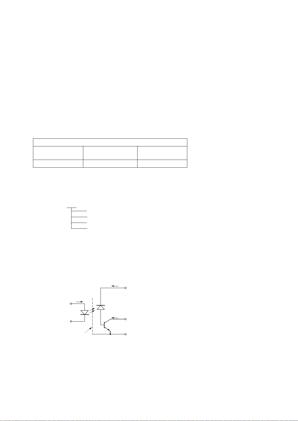
Functional Diagram
CAUTION: It is advised that normal static precautions be taken in handling and assembly of this component to
prevent damage and/or degradation which may be induced by ESD.
A 0.1 µF bypass capacitor between pins 5 and 8 is recommended.
7
1
2
3
4
5
6
8
NC
ANODE
CATHODE
NC
V
CC
NC
V
O
GND
TRUTH TABLE
LED
ON
OFF
V
O
LOW
HIGH
Description
These optocouplers are similar to
HP’s other high speed transistor
optocouplers but with shorter
propagation delays and higher
CTR. The HCPL-4504/0454 and
HCNW4504 also have a guaranteed propagation delay difference
(t
PLH
- t
PHL
). These features make
these optocouplers an excellent
solution to IPM inverter dead time
and other switching problems.
5965-3604E
Page 2
1-34
The HCPL-4504/0454 and
HCNW4504 CTR, propagation
delay, and CMR are specified for
both TTL and IPM load/drive
conditions. Specifications and
typical performance plots for both
TTL and IPM conditions are
provided for ease of application.
These single channel, diodetransistor optocouplers are
available in 8-Pin DIP, SO-8, and
Widebody package configurations. An insulating layer between
a LED and an integrated
photodetector provide electrical
insulation between input and
output. Separate connections for
Selection Guide
Single Channel Packages
8-Pin DIP Small Outline Widebody
(300 Mil) SO-8 (400 Mil)
HCPL-4504 HCPL-0454 HCNW4504
Ordering Information
Specify Part Number followed by Option Number (if desired).
Example:
HCPL-4504#XXX
020 = UL 5000 V rms/1 Minute Option*
060 = VDE 0884 V
IORM
= 630 V peak Option*
300 = Gull Wing Surface Mount Option†
500 = Tape and Reel Packaging Option
Option data sheets available. Contact your Hewlett-Packard sales representative or authorized distributor for
information.
*For HCPL-4504 only. Combination of Option 020 and Option 060 is not available.
†Gull wing surface mount option applies to through hole parts only.
Schematic
I
F
SHIELD
8
6
5
GND
V
CC
2
3
V
O
I
CC
V
F
I
O
ANODE
CATHODE
+
–
the photodiode bias and outputtransistor collector increase the
speed up to a hundred times that
of a conventional phototransistor
coupler by reducing the base
collector capacitance.
Page 3
1-35
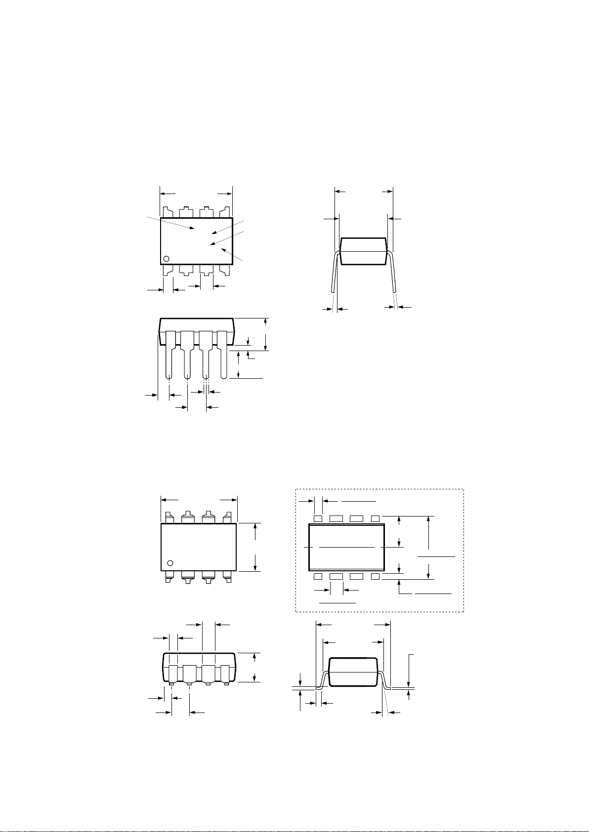
Package Outline Drawings
8-Pin DIP Package (HCPL-4504)
8-Pin DIP Package with Gull Wing Surface Mount Option 300 (HCPL-4504)
0.635 ± 0.25
(0.025 ± 0.010)
12° NOM.
9.65 ± 0.25
(0.380 ± 0.010)
0.635 ± 0.130
(0.025 ± 0.005)
7.62 ± 0.25
(0.300 ± 0.010)
5
6
7
8
4
3
2
1
9.65 ± 0.25
(0.380 ± 0.010)
6.350 ± 0.25
(0.250 ± 0.010)
1.016 (0.040)
1.194 (0.047)
1.194 (0.047)
1.778 (0.070)
9.398 (0.370)
9.906 (0.390)
4.826
(0.190)
TYP.
0.381 (0.015)
0.635 (0.025)
PAD LOCATION (FOR REFERENCE ONLY)
1.080 ± 0.320
(0.043 ± 0.013)
4.19
(0.165)
MAX.
1.780
(0.070)
MAX.
1.19
(0.047)
MAX.
2.54
(0.100)
BSC
DIMENSIONS IN MILLIMETERS (INCHES).
LEAD COPLANARITY = 0.10 mm (0.004 INCHES).
0.254
+ 0.076
- 0.051
(0.010
+ 0.003)
- 0.002)
9.65 ± 0.25
(0.380 ± 0.010)
1.78 (0.070) MAX.
1.19 (0.047) MAX.
HP XXXXZ
YYWW
DATE CODE
1.080 ± 0.320
(0.043 ± 0.013)
2.54 ± 0.25
(0.100 ± 0.010)
0.51 (0.020) MIN.
0.65 (0.025) MAX.
4.70 (0.185) MAX.
2.92 (0.115) MIN.
DIMENSIONS IN MILLIMETERS AND (INCHES).
5678
4321
5° TYP.
OPTION CODE*
UL
RECOGNITION
UR
0.254
+ 0.076
- 0.051
(0.010
+ 0.003)
- 0.002)
7.62 ± 0.25
(0.300 ± 0.010)
6.35 ± 0.25
(0.250 ± 0.010)
TYPE NUMBER
* MARKING CODE LETTER FOR OPTION NUMBERS.
"L" = OPTION 020
"V" = OPTION 060
OPTION NUMBERS 300 AND 500 NOT MARKED.
Page 4
1-36
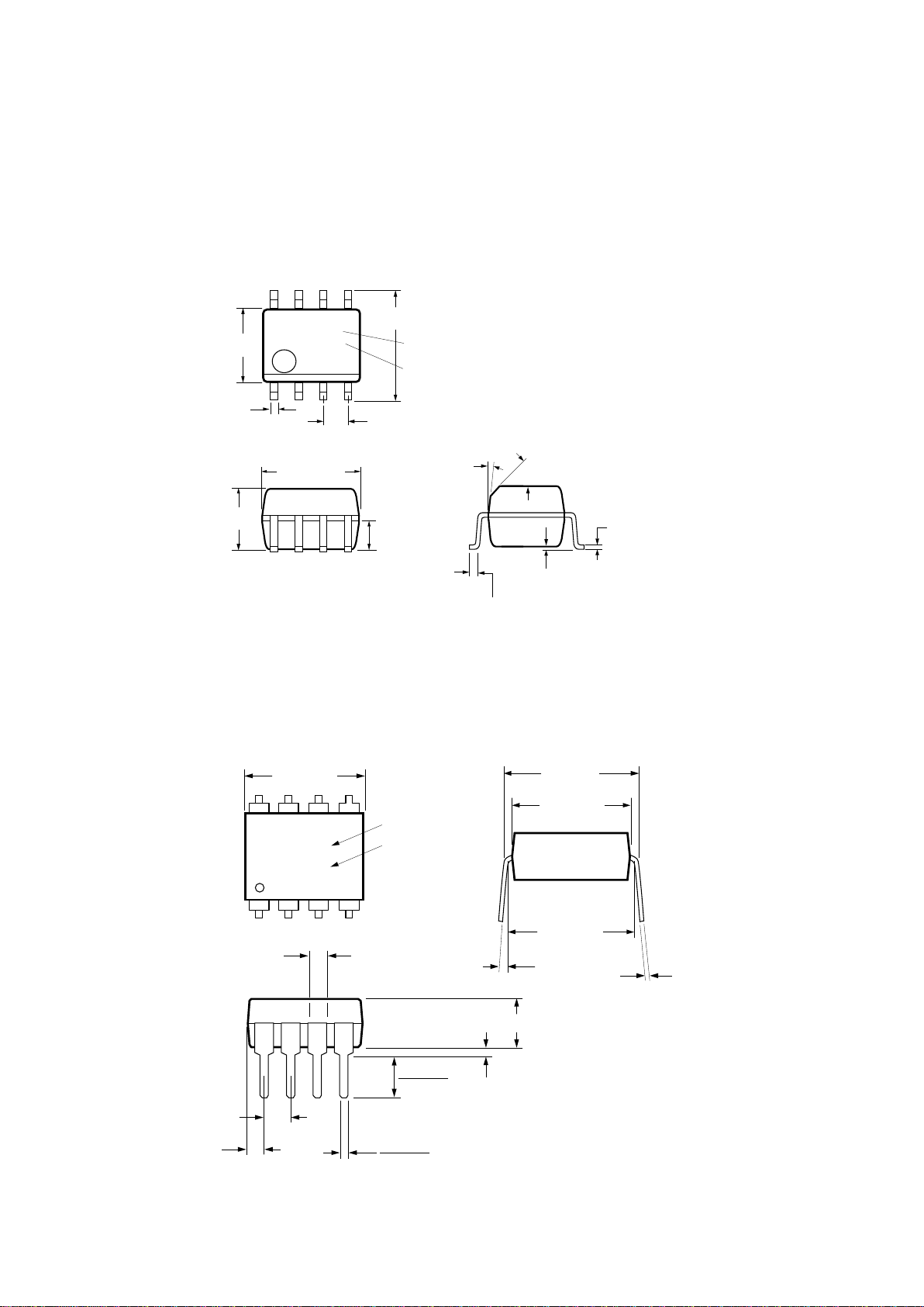
Small Outline SO-8 Package (HCPL-0454)
8-Pin Widebody DIP Package (HCNW4504)
XXX
YWW
8765
4321
5.842 ± 0.203
(0.236 ± 0.008)
3.937 ± 0.127
(0.155 ± 0.005)
0.381 ± 0.076
(0.016 ± 0.003)
1.270
(0.050)
BSG
5.080 ± 0.127
(0.200 ± 0.005)
3.175 ± 0.127
(0.125 ± 0.005)
1.524
(0.060)
45° X
0.432
(0.017)
0.228 ± 0.025
(0.009 ± 0.001)
TYPE NUMBER
(LAST 3 DIGITS)
DATE CODE
0.305
(0.012)
MIN.
DIMENSIONS IN MILLIMETERS (INCHES).
LEAD COPLANARITY = 0.10 mm (0.004 INCHES).
0.152 ± 0.051
(0.006 ± 0.002)
7°
5
6
7
8
4
3
2
1
11.15 ± 0.15
(0.442 ± 0.006)
1.78 ± 0.15
(0.070 ± 0.006)
5.10
(0.201)
MAX.
1.55
(0.061)
MAX.
2.54 (0.100)
TYP.
DIMENSIONS IN MILLIMETERS (INCHES).
7° TYP.
0.254
+ 0.076
- 0.0051
(0.010
+ 0.003)
- 0.002)
11.00
(0.433)
9.00 ± 0.15
(0.354 ± 0.006)
MAX.
10.16 (0.400)
TYP.
HP
HCNWXXXX
YYWW
DATE CODE
TYPE NUMBER
0.51 (0.021) MIN.
0.40 (0.016)
0.56 (0.022)
3.10 (0.122)
3.90 (0.154)
Page 5
1-37
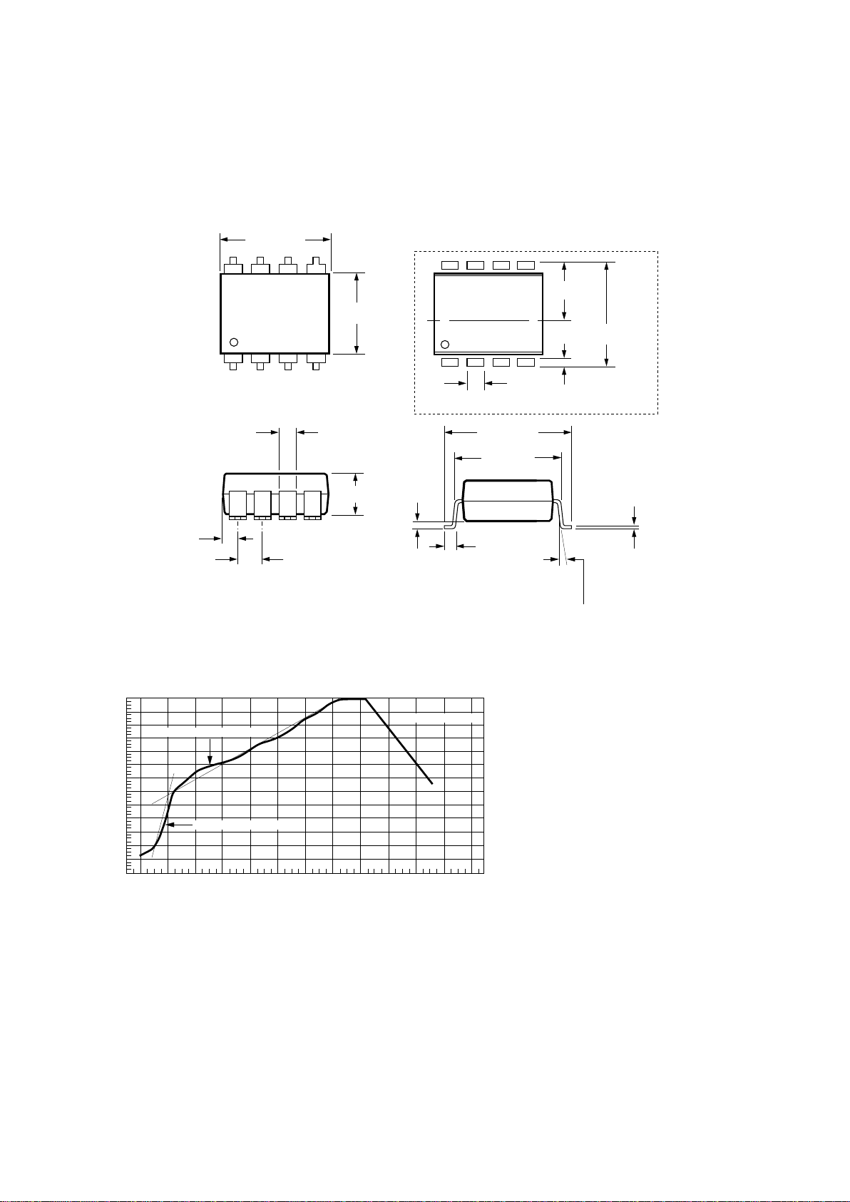
8-Pin Widebody DIP Package with Gull Wing Surface Mount Option 300 (HCNW4504)
Note: Use of nonchlorine activated fluxes is highly recommended.
240
∆T = 115°C, 0.3°C/SEC
0
∆T = 100°C, 1.5°C/SEC
∆T = 145°C, 1°C/SEC
TIME – MINUTES
TEMPERATURE – °C
220
200
180
160
140
120
100
80
60
40
20
0
260
123456789101112
Solder Reflow Temperature Profile
(HCPL-0454 and Gull Wing Surface Mount Option Parts)
1.00 ± 0.15
(0.039 ± 0.006)
7° NOM.
12.30 ± 0.30
(0.484 ± 0.012)
0.75 ± 0.25
(0.030 ± 0.010)
11.00
(0.433)
5
6
7
8
4
3
2
1
11.15 ± 0.15
(0.442 ± 0.006)
9.00 ± 0.15
(0.354 ± 0.006)
1.3
(0.051)
12.30 ± 0.30
(0.484 ± 0.012)
6.15
(0.242)
TYP.
0.9
(0.035)
PAD LOCATION (FOR REFERENCE ONLY)
1.78 ± 0.15
(0.070 ± 0.006)
4.00
(0.158)
MAX.
1.55
(0.061)
MAX.
2.54
(0.100)
BSC
DIMENSIONS IN MILLIMETERS (INCHES).
LEAD COPLANARITY = 0.10 mm (0.004 INCHES).
0.254
+ 0.076
- 0.0051
(0.010
+ 0.003)
- 0.002)
MAX.
Page 6

1-38
Insulation and Safety Related Specifications
8-Pin DIP Widebody
(300 Mil) SO-8 (400 Mil)
Parameter Symbol Value Value Value Units Conditions
Minimum External L(101) 7.1 4.9 9.6 mm Measured from input terminals
Air Gap (External to output terminals, shortest
Clearance) distance through air.
Minimum External L(102) 7.4 4.8 10.0 mm Measured from input terminals
Tracking (External to output terminals, shortest
Creepage) distance path along body.
Minimum Internal 0.08 0.08 1.0 mm Through insulation distance,
Plastic Gap conductor to conductor, usually
(Internal Clearance) the direct distance between the
photoemitter and photodetector
inside the optocoupler cavity.
Minimum Internal NA NA 4.0 mm Measured from input terminals
Tracking (Internal to output terminals, along
Creepage) internal cavity.
Tracking Resistance CTI 200 200 200 Volts DIN IEC 112/VDE 0303 Part 1
(Comparative
Tracking Index)
Isolation Group IIIa IIIa IIIa Material Group
(DIN VDE 0110, 1/89, Table 1)
Option 300 - surface mount classification is Class A in accordance with CECC 00802.
Regulatory Information
The devices contained in this data
sheet have been approved by the
following organizations:
UL
Recognized under UL 1577,
Component Recognition
Program, File E55361.
CSA
Approved under CSA Component
Acceptance Notice #5, File CA
88324.
VDE
Approved according to VDE
0884/06.92 (HCNW4504 and
HCPL-4504#060 only).
BSI
Certification according to
BS451:1994,
(BS EN60065:1994);
BS EN60950:1992
(BS7002:1992) and
EN41003:1993 for Class II
applications (HCNW4504 only).
Page 7

1-39
VDE 0884 Insulation Related Characteristics
(HCPL-4504 OPTION 060 ONLY)
Description Symbol Characteristic Units
Installation classification per DIN VDE 0110/1.89, Table 1
for rated mains voltage ≤ 300 V rms I-IV
for rated mains voltage ≤ 450 V rms I-III
Climatic Classification 55/100/21
Pollution Degree (DIN VDE 0110/1.89) 2
Maximum Working Insulation Voltage V
IORM
630 V peak
Input to Output Test Voltage, Method b*
V
IORM
x 1.875 = VPR, 100% Production Test with tm = 1 sec, V
PR
1181 V peak
Partial Discharge < 5 pC
Input to Output Test Voltage, Method a*
V
IORM
x 1.5 = VPR, Type and sample test, V
PR
945 V peak
tm = 60 sec, Partial Discharge < 5 pC
Highest Allowable Overvoltage*
(Transient Overvoltage, t
ini
= 10 sec) V
IOTM
6000 V peak
Safety Limiting Values
(Maximum values allowed in the event of a failure,
also see Figure 15, Thermal Derating curve.)
Case Temperature T
S
175 °C
Input Current I
S,INPUT
230 mA
Output Power P
S,OUTPUT
600 mW
Insulation Resistance at TS, VIO = 500 V R
S
≥ 10
9
Ω
VDE 0884 Insulation Related Characteristics (HCNW4504 ONLY)
Description Symbol Characteristic Units
Installation classification per DIN VDE 0110/1.89, Table 1
for rated mains voltage ≤ 600 V rms I-IV
for rated mains voltage ≤ 1000 V rms I-III
Climatic Classification 55/85/21
Pollution Degree (DIN VDE 0110/1.89) 2
Maximum Working Insulation Voltage V
IORM
1414 V peak
Input to Output Test Voltage, Method b*
V
IORM
x 1.875 = VPR, 100% Production Test with tm = 1 sec, V
PR
2652 V peak
Partial Discharge < 5 pC
Input to Output Test Voltage, Method a*
V
IORM
x 1.5 = VPR, Type and sample test, V
PR
2121 V peak
tm = 60 sec, Partial Discharge < 5 pC
Highest Allowable Overvoltage*
(Transient Overvoltage, t
ini
= 10 sec) V
IOTM
8000 V peak
Safety Limiting Values
(Maximum values allowed in the event of a failure,
also see Figure 15, Thermal Derating curve.)
Case Temperature T
S
150 °C
Input Current I
S,INPUT
400 mA
Output Power P
S,OUTPUT
700 mW
Insulation Resistance at TS, VIO = 500 V R
S
≥ 10
9
Ω
*Refer to the front of the optocoupler section of the current catalog under Product Safety Regulations section (VDE 0884), for a
detailed description.
Note: Isolation characteristics are guaranteed only within the safety maximum ratings which must be ensured by protective circuits in
application.
Page 8

1-40
Absolute Maximum Ratings
Parameter Symbol Device Min. Max. Units Note
Storage Temperature T
S
-55 125 °C
Operating Temperature T
A
HCPL-4504 -55 100 °C
HCPL-0454
HCNW4504 -55 85
Average Forward Input Current I
F(AVG)
25 mA 1
Peak Forward Input Current I
F(PEAK)
HCPL-4504
(50% duty cycle, 1 ms pulse width) HCPL-0454 50 mA 2
(50% duty cycle, 1 ms pulse width) HCNW4504 40
Peak Transient Input Current I
F(TRANS)
HCPL-4504 1 A
(≤ 1 µs pulse width, 300 pps) HCPL-0454
HCNW4504 0.1
Reverse LED Input Voltage (Pin 3-2) V
R
HCPL-4504 5 V
HCPL-0454
HCNW4504 3
Input Power Dissipation P
IN
HCPL-4504 45 mW 3
HCPL-0454
HCNW4504 40
Average Output Current (Pin 6) I
O(AVG)
8mA
Peak Output Current I
O(PEAK)
16 mA
Supply Voltage (Pin 8-5) V
CC
-0.5 30 V
Output Voltage (Pin 6-5) V
O
-0.5 20 V
Output Power Dissipation P
O
100 mW 4
Lead Solder Temperature
(Through-Hole Parts Only)
1.6 mm below seating plane, T
LS
HCPL-4504 260 °C
10 seconds up to seating plane, 10 seconds
Reflow Temperature Profile T
RP
HCPL-0454
and
Option 300
See Package Outline
Drawings section
HCNW4504 260 °C
Page 9

1-41
Parameter Symbol Device Min. Typ.* Max. Units Test Conditions Fig. Note
Current CTR HCPL-4504 25 32 60 % TA = 25°CVO = 0.4 V IF = 16 mA, 1, 2, 5
Transfer Ratio HCPL-0454 21 34 VO = 0.5 V VCC = 4.5 V 4
HCNW4504 23 29 60 TA = 25°CVO = 0.4 V
19 31 63 VO = 0.5 V
Current CTR HCPL-4504 26 35 65 % TA = 25°CVO = 0.4 V IF = 12 mA, 1, 2, 5
Transfer Ratio HCPL-0454 22 37 VO = 0.5 V VCC = 4.5 V 4
HCNW4504 25 33 65 TA = 25°CVO = 0.4 V
21 35 68 VO = 0.5 V
Logic Low V
OL
HCPL-4504 0.2 0.4 V TA = 25°CIO = 4.0 mA IF = 16 mA,
Output Voltage HCPL-0454 0.5 IO = 3.3 mA VCC = 4.5 V
HCNW4504 0.2 0.4 TA = 25°CIO = 3.6 mA
0.5 IO = 3.0 mA
Logic High I
OH
0.003 0.5 µATA = 25°CVO = VCC = 5.5 V IF = 0 mA 5
Output Current 0.01 1 TA = 25°CVO = VCC = 15 V
50
Logic Low I
CCL
50 200 µAIF = 16 mA, VO = Open, VCC = 15 V 12
Supply Current
Logic High I
CCH
0.02 1 µATA = 25°CIF = 0 mA, VO = Open, 12
Supply Current 2 VCC = 15 V
Input Forward V
F
HCPL-4504 1.5 1.7 V TA = 25°CIF = 16 mA 3
Voltage HCPL-0454 1.8
HCNW4504 1.45 1.59 1.85 TA = 25°CIF = 16 mA
1.35 1.95
Input Reverse BV
R
HCPL-4504 5 V IR = 10 µA
Breakdown HCPL-0454
Voltage HCNW4504 3 IR = 100 µA, TA = 25°C
Temperature ∆V
F
HCPL-4504 -1.6 mV/°CIF = 16 mA
Coefficient of ∆T
A
HCPL-0454
Forward Voltage HCNW4504 -1.4
Input C
IN
HCPL-4504 60 pF f = 1 MHz, VF = 0 V
Capacitance HCPL-0454
HCNW4504 70
*All typicals at TA = 25°C.
Electrical Specifications (DC)
Over recommended temperature (TA = 0°C to 70°C) unless otherwise specified. See note 12.
Page 10

1-42
AC Switching Specifications
Over recommended temperature (TA = 0°C to 70°C) unless otherwise specified.
Parameter Symbol Min. Typ. Max. Units Test Conditions Fig. Note
Propagation 0.2 0.3 TA = 25°C Pulse: f = 20 kHz, 6,
Delay Time t
PHL
µs Duty Cycle = 10%, 8, 9 9
to Logic Low 0.2 0.5 I
F
= 16 mA, VCC = 5.0 V,
at Output R
L
= 1.9 kΩ, CL = 15 pF,
V
THHL
= 1.5 V
0.2 0.5 0.7 T
A
= 25°C Pulse: f = 10 kHz, 6,
Duty Cycle = 50%, 10-14 10
0.1 0.5 1.0 I
F
= 12 mA, VCC = 15.0 V,
R
L
= 20 kΩ, CL = 100 pF,
V
THHL
= 1.5 V
Propagation 0.3 0.5 TA = 25°C Pulse: f = 20 kHz, 6,
Delay Time t
PLH
µs Duty Cycle = 10%, 8, 9 9
to Logic 0.3 0.7 I
F
= 16 mA, VCC = 5.0 V,
High at R
L
= 1.9 kΩ, CL = 15 pF,
Output V
THLH
= 1.5 V
0.3 0.8 1.1 T
A
= 25°C Pulse: f = 10 kHz, 6,
Duty Cycle = 50%, 10-14 10
0.2 0.8 1.4 I
F
= 12 mA, VCC = 15.0 V,
R
L
= 20 kΩ, CL = 100 pF,
V
THLH
= 2.0 V
Propagation -0.4 0.3 0.9 TA = 25°C Pulse: f = 10 kHz, 6,
Delay t
PLH-tPHL
µs Duty Cycle = 50%, 10-14 15
Difference -0.7 0.3 1.3 I
F
= 12 mA, VCC = 15.0 V,
Between R
L
= 20 kΩ, CL = 100 pF,
Any 2 Parts V
THHL
= 1.5 V, V
THLH
= 2.0 V
Common VCC = 5.0 V, RL = 1.9 kΩ,
Mode 15 30 C
L
= 15 pF, IF = 0 mA 7 7, 9
Transient |CM
H
| kV/µsTA = 25°C
Immunity at 15 30 V
CC
= 15.0 V, RL = 20 kΩ,
Logic High V
CM
=C
L
= 100 pF, IF = 0 mA 7 8, 10
Level Output 1500 V
P-P
Common VCC = 5.0 V, RL = 1.9 kΩ,
Mode 15 30 C
L
= 15 pF, IF = 16 mA 7 7, 9
Transient |CM
L
| kV/µsTA = 25°C
Immunity at 10 30 V
CC
= 15.0 V, RL = 20 kΩ,
Logic Low V
CM
=C
L
= 100 pF, IF = 12 mA 7 8, 10
Level Output 1500 V
P-P
15 30 VCC = 15.0 V, RL = 20 kΩ, 7 8, 10
C
L
= 100 pF, IF = 16 mA
*All typicals at TA = 25°C.
7 8, 10
Page 11

1-43
Package Characteristics
Over recommended temperature (TA = 0°C to 25°C) unless otherwise specified.
Parameter Sym. Device Min. Typ.* Max. Units Test Conditions Fig. Note
Input-Output V
ISO
HCPL-4504 2500 V rms RH ≤ 50%, 6, 13
Momentary HCPL-0454 t = 1 min.,
Withstand TA = 25° C
Voltage†
HCPL-4504 5000 6, 11,
(Option 020) 14
Input-Output R
I-O
HCPL-4504 10
12
Ω V
I-O
= 500 Vdc 6
Resistance HCPL-0454
HCNW4504 10
12
10
13
TA = 25° C
10
11
TA = 100° C
Input-Output C
I-O
HCPL-4504 0.6 pF f = 1 MHz 6
Capacitance HCPL-0454
HCNW4504 0.5 0.6
*All typicals at TA = 25°C..
†The Input-Output Momentary Withstand Voltage is a dielectric voltage rating that should not be interpreted as an input-output
continuous voltage rating. For the continuous voltage rating refer to the VDE 0884 Insulation Related Characteristics Table (if
applicable), your equipment level safety specification or HP Application Note 1074 entitled “Optocoupler Input-Output Endurance
Voltage.”
HCNW4504 5000
Notes:
1. Derate linearly above 70°C free-air temperature at a rate of 0.8 mA/°C (8-Pin DIP).
Derate linearly above 85°C free-air temperature at a rate of 0.5 mA/°C (SO-8).
2. Derate linearly above 70°C free-air temperature at a rate of 1.6 mA/°C (8-Pin DIP).
Derate linearly above 85°C free-air temperature at a rate of 1.0 mA/°C (SO-8).
3. Derate linearly above 70°C free-air temperature at a rate of 0.9 mW/°C (8-Pin DIP).
Derate linearly above 85°C free-air temperature at a rate of 1.1 mW/°C (SO-8).
4. Derate linearly above 70°C free-air temperature at a rate of 2.0 mW/°C (8-Pin DIP).
Derate linearly above 85°C free-air temperature at a rate of 2.3 mW/°C (SO-8).
5. CURRENT TRANSFER RATIO in percent is defined as the ratio of output collector current, IO, to the forward LED input current,
IF, times 100.
6. Device considered a two-terminal device: Pins 1, 2, 3, and 4 shorted together and Pins 5, 6, 7, and 8 shorted together.
7. Under TTL load and drive conditions: Common mode transient immunity in a Logic High level is the maximum tolerable (positive)
dVCM/dt on the leading edge of the common mode pulse, VCM, to assure that the output will remain in a Logic High state
(i.e., VO> 2.0 V). Common mode transient immunity in a Logic Low level is the maximum tolerable (negative) dVCM/dt on the
trailing edge of the common mode pulse signal, VCM, to assure that the output will remain in a Logic Low state (i.e., VO < 0.8 V).
6, 14
8. Under IPM (Intelligent Power Module) load and LED drive conditions: Common mode transient immunity in a Logic High level is
the maximum tolerable dVCM/dt on the leading edge of the common mode pulse, VCM, to assure that the output will remain in a
Logic High state (i.e., VO > 3.0 V). Common mode transient immunity in a Logic Low level is the maximum tolerable dVCM/dt on
the trailing edge of the common mode pulse signal, VCM, to assure that the output will remain in a Logic Low state
(i.e., VO< 1.0 V).
9. The 1.9 kΩ load represents 1 TTL unit load of 1.6 mA and the 5.6 kΩ pull-up resistor.
10. The RL = 20 kΩ, CL = 100 pF load represents an IPM (Intelligent Power Module) load.
11. See Option 020 data sheet for more information.
12. Use of a 0.1 µF bypass capacitor connected between pins 5 and 8 is recommended.
13. In accordance with UL 1577, each optocoupler is proof tested by applying an insulation test voltage ≥ 3000 V rms for 1 second
(leakage detection current limit, I
i-o
≤ 5 µA). This test is performed before the 100% Production test shown in the VDE 0884
Insulation Related Characteristics Table, if applicable.
14. In accordance with UL 1577, each optocoupler is proof tested by applying an insulation test voltage ≥ 6000 V rms for 1 second
(leakage detection current limit, I
i-o
≤ 5 µA). This test is performed before the 100% Production test shown in the VDE 0884
Insulation Related Characteristics Table, if applicable.
15. The difference between t
PLH
and t
PHL
between any two devices (same part number) under the same test condition. (See Power
Inverter Dead Time and Propagation Delay Specifications section.)
Page 12

1-44
Figure 1. DC and Pulsed Transfer Characteristics.
Figure 2. Current Transfer Ratio vs. Input Current.
Figure 3. Input Current vs. Forward Voltage.
0
10
20
V
O
– OUTPUT VOLTAGE – V
I
O
– OUTPUT CURRENT – mA
20
10
0
T = 25°C
V = 5.0 V
A
CC
40 mA
35 mA
30 mA
25 mA
20 mA
15 mA
10 mA
I = 5 mA
F
HCNW4504
2
4
6
8
12
14
16
18
IF – INPUT CURRENT – mA
NORMALIZED CURRENT TRANSFER RATIO
1.6
0.8
0
510150
20 25
IF = 16 mA
VO = 0.4 V
V
CC
= 5.0 V
T
A
= 25°C
NORMALIZED
HCNW4504
0.4
1.2
2.0
0
10
20
V
O
– OUTPUT VOLTAGE – V
I
O
– OUTPUT CURRENT – mA
10
5
0
T = 25°C
V = 5.0 V
A
CC
40 mA
35 mA
30 mA
25 mA
20 mA
15 mA
10 mA
I = 5 mA
F
HCPL-4504/0454
IF – INPUT CURRENT – mA
NORMALIZED CURRENT TRANSFER RATIO
1.5
1.0
0.5
0.0
2 4 6 8 10 12 14 16
180202224 26
IF = 16 mA
V
O
= 0.4 V
V
CC
= 5.0 V
T
A
= 25°C
NORMALIZED
HCPL-4504/0454
VF – FORWARD VOLTAGE – VOLTS
100
10
0.1
0.01
1.1 1.2 1.3 1.4
I
F
– FORWARD CURRENT – mA
1.61.5
1.0
0.001
1000
I
F
V
F
+
T = 25°C
A
–
HCPL-4504/0454
VF – FORWARD VOLTAGE – VOLTS
100
10
0.1
0.01
1.2 1.3 1.4 1.5
I
F
– FORWARD CURRENT – mA
1.71.6
1.0
0.001
1000
I
F
V
F
+
T = 25°C
A
–
HCNW4504
Page 13

1-45
Figure 6. Switching Test Circuit.
Figure 4. Current Transfer Ratio vs. Temperature. Figure 5. Logic High Output Current
vs. Temperature.
TA – TEMPERATURE – °C
I
OH
– LOGIC HIGH OUTPUT CURRENT – nA
10
4
10
3
10
2
10
1
10
0
10
-1
10
-2
-40 -20 0 20 40 60 80 100
120
-60
IF = 0 mA
VO = VCC = 5.0 V
V
O
PULSE
GEN.
Z = 50 Ω
t = 5 ns
O
r
I MONITOR
F
I
F
0.1µF
L
R
C
L
R
M
0
t
PHL
t
PLH
O
V
I
F
OL
V
THHL
V
THLH
V
V
CC
V
CC
1
2
3
4
8
7
6
5
Figure 7. Test Circuit for Transient Immunity and Typical Waveforms.
TA – TEMPERATURE – °C
NORMALIZED CURRENT TRANSFER RATIO
1.0
0.9
0.85
1.05
0.95
-40
-20020
40 60 80 100 120-60
IF = 16 mA
V
O
= 0.4 V
V
CC
= 5.0 V
T
A
= 25°C
NORMALIZED
HCNW4504
TA – TEMPERATURE – °C
NORMALIZED CURRENT TRANSFER RATIO
1.0
0.8
0.6
1.1
0.7
0.9
-40
-20020
40 60 80 100 120-60
IF = 16 mA
VO = 0.4 V
V
CC
= 5.0 V
TA = 25°C
NORMALIZED
HCPL-4504/0454
V
O
I
F
0.1µF
L
R
A
B
PULSE GEN.
V
CM
+
V
FF
L
C
O
V
OL
V
O
V
0 V
10%
90% 90%
10%
SWITCH AT A: I = 0 mA
F
SWITCH AT B: I = 12 mA, 16 mA
F
CM
V
t
r
t
f
CC
V
V
CC
–
1
2
3
4
8
7
6
5
Page 14

1-46
RL – LOAD RESISTANCE – kΩ
t
p
– PROPAGATION DELAY – µs
1.6
1.4
1.2
1.0
0.6
0.2
0.0
510152025303540450
VCC = 15.0 V
T
A
= 25° C
C
L
= 100 pF
V
THHL
= 1.5 V
V
THLH
= 2.0 V
50
t
PLH
t
PHL
1.8
0.4
0.8
IF = 10 mA
I
F
= 16 mA
50% DUTY CYCLE
RL– LOAD RESISTANCE – kΩ
t
p
– PROPAGATION DELAY – µs
1.4
1.2
1.0
0.8
0.6
0.4
0.2
0.0
2 4 6 8 10 12 14 16 180
20
1.6
1.8
2.0
2.2
2.4
2.6
VCC = 5.0 V
T
A
= 25° C
C
L
= 100 pF
V
THHL
= 1.5 V
V
THLH
= 2.0 V
IF = 10 mA
I
F
= 16 mA
t
PLH
t
PHL
50% DUTY CYCLE
RL – LOAD RESISTANCE – kΩ
t
p
– PROPAGATION DELAY – µs
1.4
1.2
1.0
0.8
0.6
0.4
0.2
0.0
2 4 6 8 10 12 14 16
18
0
20
t
PHL
VCC = 5.0 V
T
A
= 25° C
C
L
= 15 pF
V = V = 1.5 V
IF = 10 mA
I
F
= 16 mA
t
PLH
10% DUTY CYCLE
THHL THLH
Figure 14. Propagation Delay Time vs.
Supply Voltage.
Figure 11. Propagation Delay Time vs.
Temperature.
Figure 13. Propagation Delay Time vs.
Load Capacitance.
Figure 12. Propagation Delay Time vs.
Load Resistance.
Figure 8. Propagation Delay Time vs. Temperature.
Figure 10. Propagation Delay Time vs.
Load Resistance.
Figure 9. Propagation Delay Time vs.
Load Resistance.
RL – LOAD CAPACITANCE – pF
t
p
– PROPAGATION DELAY – µs
2.0
1.5
0.5
0.0
100 200 300 400 500 600 700 800 9000
VCC = 15.0 V
T
A
= 25° C
R
L
= 20 kΩ
V
THHL
= 1.5 V
V
THLH
= 2.0 V
1000
t
PLH
t
PHL
2.5
3.0
3.5
1.0
IF = 10 mA
I
F
= 16 mA
50% DUTY CYCLE
V
CC
– SUPPLY VOLTAGE – V
tp – PROPAGATION DELAY – µs
0.9
0.8
0.6
0.2
11 12 13 14 15 16 17 18 1910 20
1.0
1.1
1.2
0.7
TA = 25° C
R
L
= 20 kΩ
C
L
= 100 pF
V
V
0.5
0.4
0.3
t
PLH
t
PHL
IF = 10 mA
I
F
= 16 mA
50% DUTY CYCLE
THHL
= 1.5 V
= 2.0 V
THLH
TA – TEMPERATURE – °C
t
p
– PROPAGATION DELAY – µs
0.50
0.45
0.40
0.35
0.30
0.25
0.20
0.15
0.10
-40 -20 0 20 40 60 80 100
120
-60
VCC = 5.0 V
R
L
= 1.9 kΩ
C
L
= 15 pF
V
THHL
t
PLH
t
PHL
IF = 10 mA
I
F
= 16 mA
= V
THLH
= 1.5 V
10% DUTY CYCLE
HCPL-4504/0454
T
A
– TEMPERATURE – °C
t
p
– PROPAGATION DELAY – µs
1.1
1.0
0.9
0.8
0.7
0.6
0.5
0.4
0.3
-40 -20 0 20 40
60 80 100 120
-60
VCC = 15.0 V
R
L
= 20 kΩ
C
L
= 100 pF
V
THHL
= 1.5 V
V
THLH
= 2.0 V
t
PLH
t
PHL
IF = 10 mA
I
F
= 16 mA
50% DUTY CYCLE
TA – TEMPERATURE – °C
t
p
– PROPAGATION DELAY – µs
0.50
0.45
0.40
0.35
0.30
0.25
0.20
0.15
0.10
-40 -20 0 20 40 60 80 100
120
-60
VCC = 5.0 V
R
L
= 1.9 kΩ
C
L
= 15 pF
V
THHL
t
PLH
t
PHL
IF = 10 mA
I
F
= 16 mA
= V
THLH
= 1.5 V
10% DUTY CYCLE
HCNW4504
Page 15

1-47
Figure 15. Thermal Derating Curve,
Dependence of Safety Limiting Valve
with Case Temperature per VDE 0884.
Figure 16. Typical Power Inverter.
BASE/GATE
DRIVE CIRCUIT
HCPL-4504/0454
HCNW4504
2
3
8
7
6
5
+HV
Q1
LED 1
OUT 1
BASE/GATE
DRIVE CIRCUIT
2
3
8
7
6
5
–HV
Q2
LED 2
OUT 2
+
+
HCPL-4504/0454
HCNW4504
OUTPUT POWER – P
S
, INPUT CURRENT – I
S
0
0
TS – CASE TEMPERATURE – °C
175
1000
50
400
12525 75 100 150
600
800
200
100
300
500
700
900
PS (mW)
I
S
(mA)
HCNW4504
OUTPUT POWER – P
S
, INPUT CURRENT – I
S
0
0
TS – CASE TEMPERATURE – °C
20050
400
12525 75 100 150
600
800
200
100
300
500
700
PS (mW)
I
S
(mA)
HCPL-4504 OPTION 060
175
(230)
Figure 17. LED Delay and Dead Time Diagram.
LED 1
OUT 1
LED 2
OUT 2
t
PLH min
t
PLH max
t
PHL min
t
PHL max
(t
PLH max–tPLH min
)
(t
PHL max–tPHL min
)
TURN-ON DELAY
MAXIMUM DEAD TIME
(t
PLH max–tPLH min
)
Power Inverter Dead
Time and Propagation
Delay Specifications
The HCPL-4504/0454 and
HCNW4504 include a specification intended to help designers
minimize “dead time” in their
power inverter designs. The new
“propagation delay difference”
specification (t
PLH-tPHL
) is useful
for determining not only how
much optocoupler switching delay
is needed to prevent “shootthrough” current, but also for
determining the best achievable
worst-case dead time for a given
design.
When inverter power transistors
switch (Q1 and Q2 in Figure 17),
it is essential that they never
Page 16

1-48
time is the sum of the maximum
difference in turn-on delay plus
the maximum difference in turnoff delay,
[(t
PLHmax-tPLHmin
)+(t
PHLmax-tPHLmin
)].
This expression can be
rearranged to obtain
[(t
PLHmax-tPHLmin
)-(t
PHLmin-tPHLmax
)],
and further rearranged to obtain
[(t
PLH-tPHL)max
-(t
PLH-tPHL)min
],
which is the maximum minus the
minimum data sheet values of
(t
PLH-tPHL
). The difference
between the maximum and
minimum values depends directly
on the total spread in propagation
delays and sets the limit on how
good the worst-case dead time
can be for a given design.
Therefore, optocouplers with tight
propagation delay specifications
(and not just shorter delays or
lower pulse-width distortion) can
achieve short dead times in power
inverters. The HCPL-4504/0454
and HCNW4504 specify a
minimum (t
PLH-tPHL
) of -0.7 µs
over an operating temperature
range of 0-70°C, resulting in a
maximum dead time of 2.0 µs
when the LED turn-on delay is
equal to (t
PLH-tPHL
)
max
, or 1.3 µs.
It is important to maintain
accurate LED turn-on delays
because delays shorter than
(t
PLH-tPHL
)
max
may allow shootthrough currents, while longer
delays will increase the worst-case
dead time.
conduct at the same time.
Extremely large currents will flow
if there is any overlap in their
conduction during switching
transitions, potentially damaging
the transistors and even the surrounding circuitry. This “shootthrough” current is eliminated by
delaying the turn-on of one
transistor (Q2) long enough to
ensure that the opposing
transistor (Q1) has completely
turned off. This delay introduces a
small amount of “dead time” at
the output of the inverter during
which both transistors are off
during switching transitions.
Minimizing this dead time is an
important design goal for an
inverter designer.
The amount of turn-on delay
needed depends on the propagation delay characteristics of the
optocoupler, as well as the
characteristics of the transistor
base/gate drive circuit. Considering only the delay characteristics
of the optocoupler (the characteristics of the base/gate drive
circuit can be analyzed in the
same way), it is important to
know the minimum and maximum
turn-on (t
PHL
) and turn-off (t
PLH
)
propagation delay specifications,
preferably over the desired
operating temperature range. The
importance of these specifications
is illustrated in Figure 17. The
waveforms labeled “LED1”,
“LED2”, “OUT1”, and “OUT2” are
the input and output voltages of
the optocoupler circuits driving
Q1 and Q2 respectively. Most
inverters are designed such that
the power transistor turns on
when the optocoupler LED turns
on; this ensures that both power
transistors will be off in the event
of a power loss in the control
circuit. Inverters can also be
designed such that the power
transistor turns off when the
optocoupler LED turns on; this
type of design, however, requires
additional fail-safe circuitry to
turn off the power transistor if an
over-current condition is
detected. The timing illustrated in
Figure 17 assumes that the power
transistor turns on when the
optocoupler LED turns on.
The LED signal to turn on Q2
should be delayed enough so that
an optocoupler with the very
fastest turn-on propagation delay
(t
PHLmin
) will never turn on before
an optocoupler with the very
slowest turn-off propagation delay
(t
PLHmax
) turns off. To ensure this,
the turn-on of the optocoupler
should be delayed by an amount
no less than (t
PLHmax-tPHLmin
),
which also happens to be the
maximum data sheet value for the
propagation delay difference
specification, (t
PLH-tPHL
). The
HCPL-4504/0454 and
HCNW4504 specify a maximum
(t
PLH-tPHL
) of 1.3 µs over an
operating temperature range
of 0-70°C.
Although (t
PLH-tPHL
)
max
tells the
designer how much delay is
needed to prevent shoot-through
current, it is insufficient to tell the
designer how much dead time a
design will have. Assuming that
the optocoupler turn-on delay is
exactly equal to (t
PLH
- t
PHL
)
max
,
the minimum dead time is zero
(i.e., there is zero time between
the turn-off of the very slowest
optocoupler and the turn-on of
the very fastest optocoupler).
Calculating the maximum dead
time is slightly more complicated.
Assuming that the LED turn-on
delay is still exactly equal to
(t
PLH-tPHL
)
max
, it can be seen in
Figure 17 that the maximum dead
 Loading...