

Page 1
1-348
H
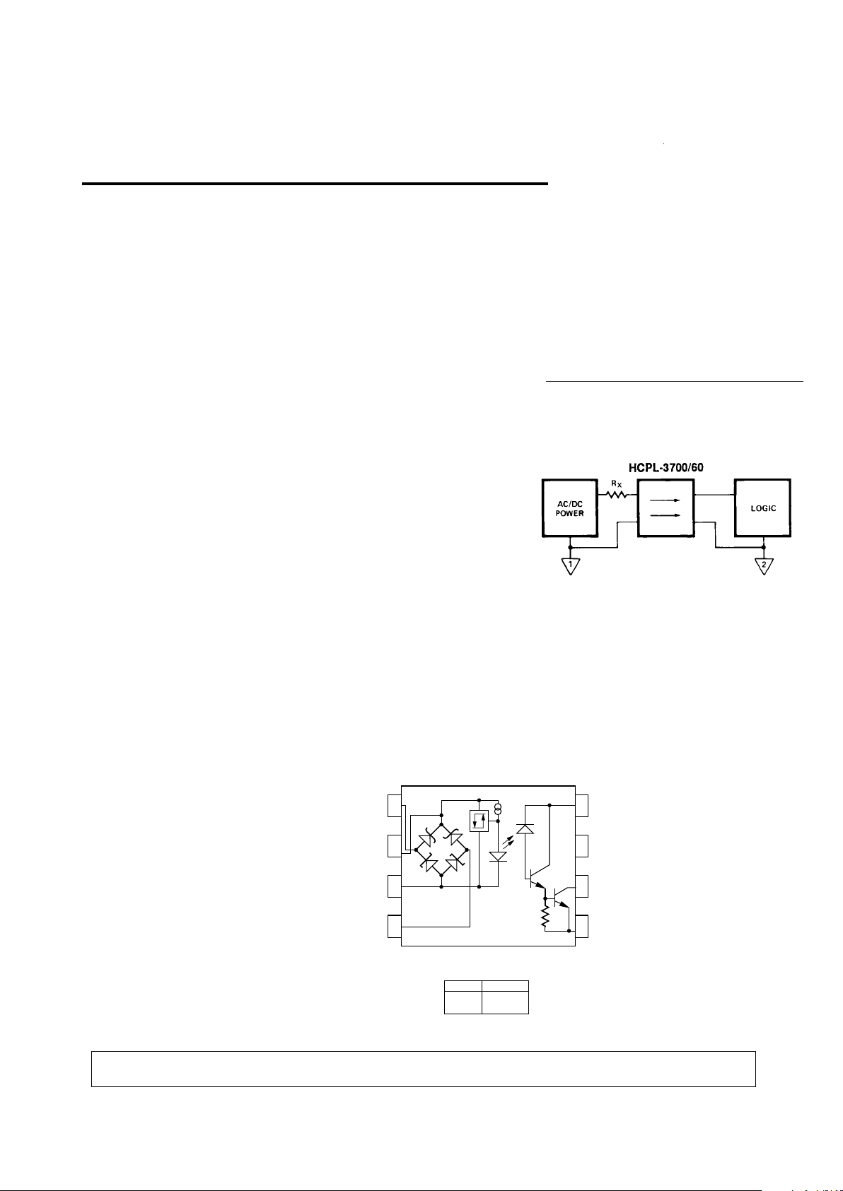
AC/DC to Logic Interface
Optocouplers
Technical Data
HCPL-3700
HCPL-3760
Description
The HCPL-3700 and HCPL-3760
are voltage/current threshold
detection optocouplers. The
HCPL-3760 is a low-current
version of the HCPL-3700. To
obtain lower current operation,
the HCPL-3760 uses a highefficiency AlGaAs LED which
provides higher light output at
lower drive currents. Both
devices utilize threshold sensing
input buffer ICs which permit
control of threshold levels over a
wide range of input voltages with
a single external resistor.
Features
• Standard (HCPL-3700) and
Low Input Current
(HCPL-3760) Versions
• AC or DC Input
• Programmable Sense Voltage
• Hysteresis
• Logic Compatible Output
• Thresholds Guaranteed over
Temperature
• Thresholds Independent of
LED Optical Parameters
• Recognized under UL 1577
and CSA Approved for
Dielectric Withstand Proof
Test Voltage of 2500 Vac, 1
Minute
Applications
• Limit Switch Sensing
• Low Voltage Detector
• 5 V-240 V AC/DC Voltage
Sensing
• Relay Contact Monitor
• Relay Coil Voltage Monitor
• Current Sensing
• Microprocessor Interfacing
CAUTION: It is advised that normal static precautions be taken in handling and assembly of this component to
prevent damage and/or degradation which may be induced by ESD.
The input buffer incorporates
several features: hysteresis for
extra noise immunity and
switching immunity, a diode
bridge for easy use with ac input
signals, and internal clamping
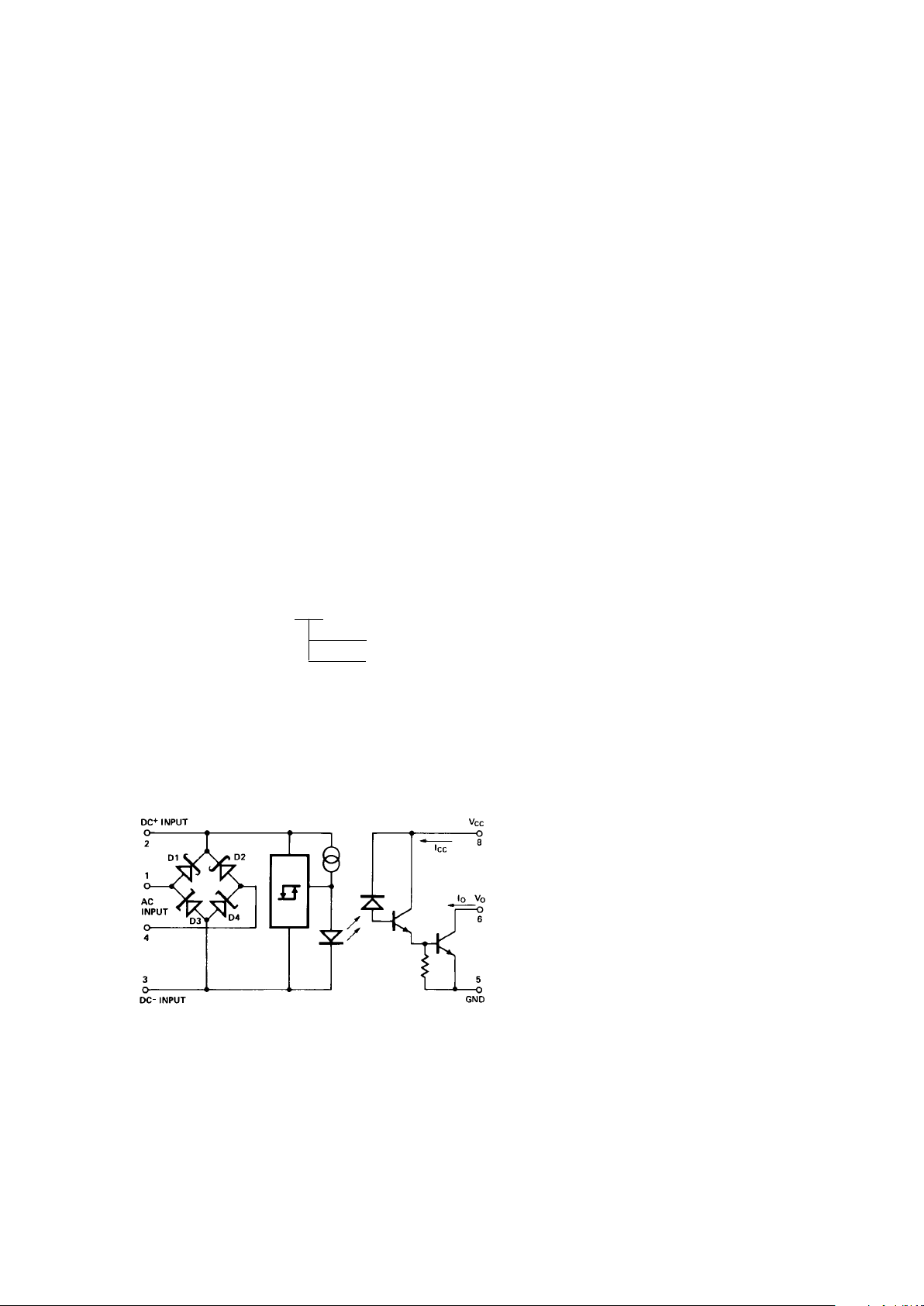
Functional Diagram
1
2
3
4
8
7
6
5
AC
DC+
DC-
AC
V
CC
V
O
GND
TRUTH TABLE
(POSITIVE LOGIC)
INPUT
H
L
OUTPUT
L
H
NC
5965-3582E
Page 2
1-349
diodes to protect the buffer and
LED from a wide range of overvoltage and over-current
transients. Because threshold
sensing is done prior to driving
the LED, variations in optical
coupling from the LED to the
detector will have no effect on the
threshold levels.
The HCPL-3700's input buffer IC
has a nominal turn on threshold
of 2.5 mA (ITH +) and 3.7 volts
(VTH +).
The buffer IC for the HCPL-3760
was redesigned to permit a lower
input current. The nominal turn
on threshold for the HCPL-3760
is 1.2 mA (ITH +) and 3.7 volts
(VTH +).
The high gain output stage
features an open collector output
providing both TTL compatible
saturation voltages and CMOS
compatible breakdown voltages.
By combining several unique
functions in a single package, the
user is provided with an ideal
component for industrial control
computer input boards and other
applications where a predetermined input threshold level is
desirable.
Ordering Information
Specify Part Number followed by Option Number (if desired)
Example
HCPL-3700#XXX
300 = Gull Wing Surface Mount Option
500 = Tape/Reel Package Option (1 K min.)
Option data sheets available. Contact your Hewlett-Packard sales representative or authorized distributor for
information.
Schematic
Page 3
1-350
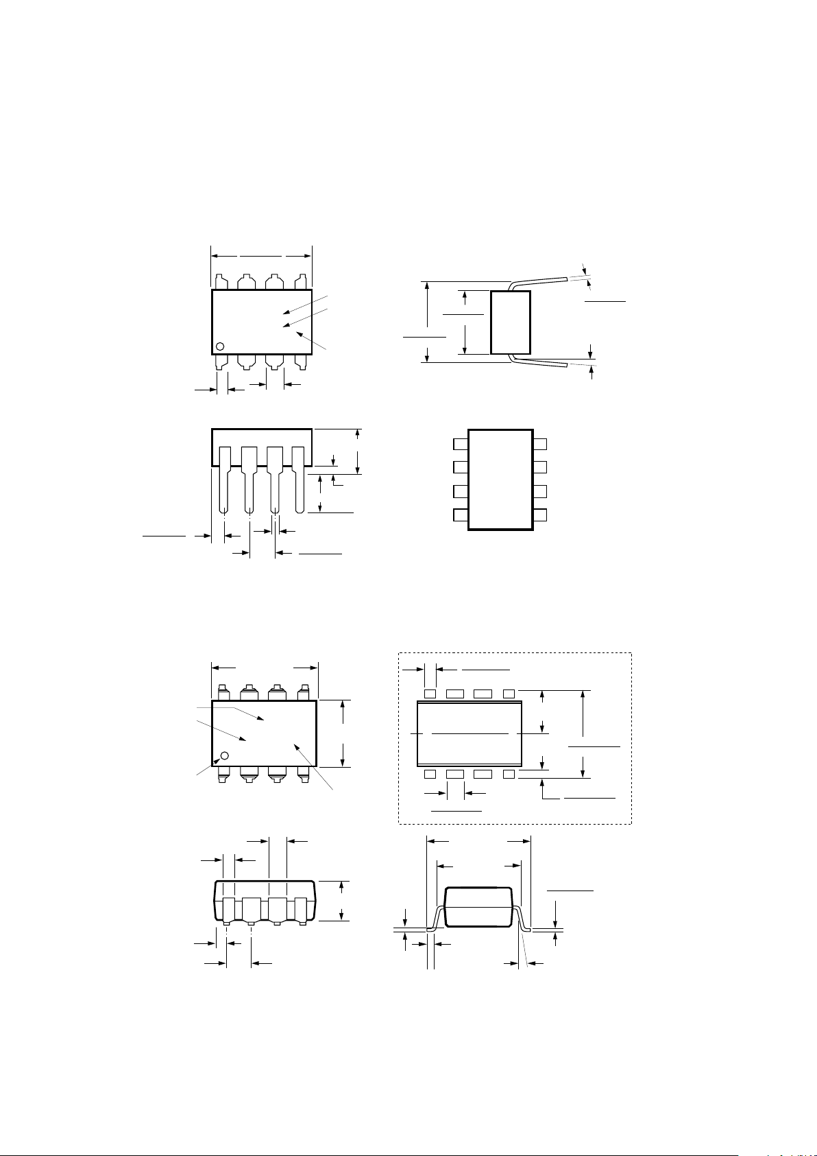
Package Outline Drawings
Standard DIP Package
Gull Wing Surface Mount Option 300
9.40 (0.370)
9.90 (0.390)
1.78 (0.070) MAX.
1.19 (0.047) MAX.
HP XXXX
YYWW
DATE CODE
0.76 (0.030)
1.40 (0.056)
2.28 (0.090)
2.80 (0.110)
0.51 (0.020) MIN.
0.65 (0.025) MAX.
4.70 (0.185) MAX.
2.92 (0.115) MIN.
DIMENSIONS IN MILLIMETERS AND (INCHES).
5678
4321
0.20 (0.008)
0.33 (0.013)
6.10 (0.240)
6.60 (0.260)
5° TYP.
7.36 (0.290)
7.88 (0.310)
1
2
3
4
8
7
6
5
AC
AC
DC+
DC-
GND
V
CC
NC
V
O
PIN ONE
TYPE NUMBER
UL
RECOGNITION
UR
0.635 ± 0.25
(0.025 ± 0.010)
12° NOM.
0.20 (0.008)
0.33 (0.013)
9.65 ± 0.25
(0.380 ± 0.010)
0.635 ± 0.130
(0.025 ± 0.005)
7.62 ± 0.25
(0.300 ± 0.010)
5
6
7
8
4
3
2
1
9.65 ± 0.25
(0.380 ± 0.010)
6.350 ± 0.25
(0.250 ± 0.010)
1.016 (0.040)
1.194 (0.047)
1.194 (0.047)
1.778 (0.070)
9.398 (0.370)
9.906 (0.390)
4.826
(0.190)
TYP.
0.381 (0.015)
0.635 (0.025)
PAD LOCATION (FOR REFERENCE ONLY)
1.080 ± 0.320
(0.043 ± 0.013)
4.19
(0.165)
MAX.
1.780
(0.070)
MAX.
1.19
(0.047)
MAX.
2.540
(0.100)
BSC
DIMENSIONS IN MILLIMETERS (INCHES).
TOLERANCES (UNLESS OTHERWISE SPECIFIED):
LEAD COPLANARITY
MAXIMUM: 0.102 (0.004)
xx.xx = 0.01
xx.xxx = 0.005
HP XXXX
YYWW
DATE CODE
TYPE NUMBER
UL
RECOGNITION
UR
MOLDED
Page 4
1-351
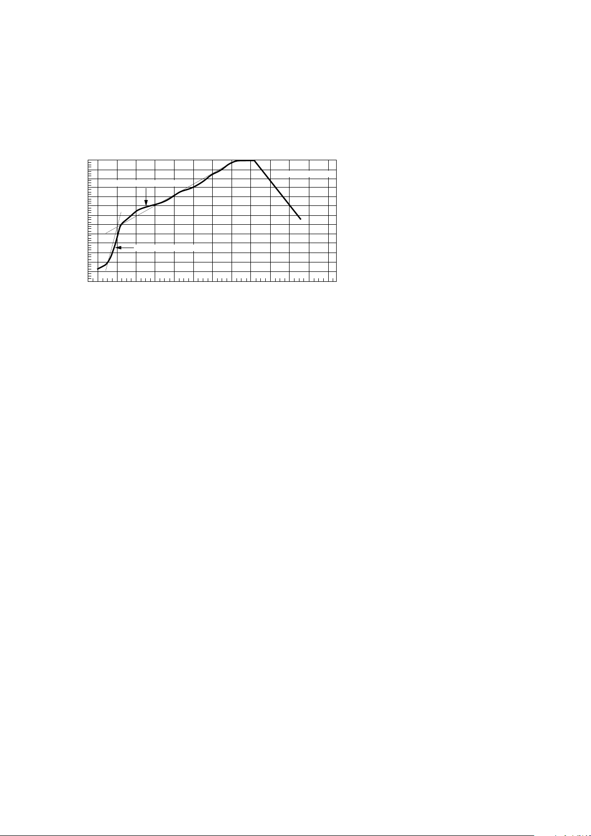
Maximum Solder Reflow Thermal Profile
240
∆T = 115°C, 0.3°C/SEC
0
∆T = 100°C, 1.5°C/SEC
∆T = 145°C, 1°C/SEC
TIME – MINUTES
TEMPERATURE – °C
220
200
180
160
140
120
100
80
60
40
20
0
260
123456789101112
(NOTE: USE OF NON-CHLORINE ACTIVATED FLUXES IS RECOMMENDED.)
Regulatory Information
The HCPL-3700/60 has been
approved by the following
organizations:
UL
Recognized under UL 1577,
component recognition program,
File E55361.
CSA
Approved under CSA Component
Acceptance Notice #5, File CA
88324.
Page 5

1-352
Insulation and Safety Related Specifications
Parameter Symbol Value Units Conditions
Min. External Air Gap L(IO1) 7.1 mm Measured from input terminals to output terminals,
(External Clearance) shortest distance through air
Min. External Tracking L(IO2) 7.4 mm Measured from input terminals to output terminals,
Path (External Creepage) shortest distance path along body
Min. Internal Plastic 0.08 mm Through insulation distance, conductor to conductor,
Gap (Internal Clearance) usually the direct distance between the photoemitter
and photodetector inside the optocoupler cavity
Tracking Resistance CTI 200 V DIN IEC 112/VDE 0303 PART 1
(Comparative
Tracking Index)
Isolation Group IIIa Material Group (DIN VDE 0110, 1/89, Table 1)
Option 300 – surface mount classification is Class A in accordance with CECC 00802.
Absolute Maximum Ratings (No derating required up to 70°C)
Parameter Symbol Min. Max. Units Note
Storage Temperature T
S
-55 125 °C
Operating Temperature T
A
-40 85 °C
Lead Soldering Cycle Temperature 260 °C1
Time 10 s
Input Current Average 50 2
Surge I
IN
140 mA 2, 3
Transient 500
Input Voltage (Pins 2-3) V
IN
-0.5 V
Input Power Dissipation P
IN
230 mW 4
Total Package Power Dissipation P
T
305 mW 5
Output Power Dissipation P
O
210 mW 6
Output Current Average I
O
30 mA 7
Supply Voltage (Pins 8-5) V
CC
-0.5 20 V
Output Voltage (Pins 6-5) V
O
-0.5 20 V
Solder Reflow Temperature Profile See Package Outline Drawings section
Recommended Operating Conditions
Parameter Symbol Min. Max. Units Note
Supply Voltage V
CC
218 V
Operating Temperature T
A
070°C
Operating Frequency f 0 4 kHz 8
Page 6

1-353
Parameter Sym. Device Min. Typ.
[9]
Max. Units Conditions Fig. Note
Input Threshold I
TH+
HCPL-3700 1.96 2.5 3.11 mA VIN = V
TH+
; VCC = 4.5 V; 2, 3 14
HCPL-3760 0.87 1.2 1.56
I
TH-
HCPL-3700 1.00 1.3 1.62 VIN = V
TH-
; VCC = 4.5 V;
HCPL-3760 0.43 0.6 0.80
Input DC V
TH+
3.35 3.7 4.05 V VIN = V2 - V3; Pins 1 & 4 Open
Threshold (Pins 2, 3) V
CC
= 4.5 V; VO = 0.4 V;
Voltage I
O
≥ 4.2 mA
V
TH-
2.01 2.6 2.86 V VIN = V2 - V3; Pins 1 & 4 Open
V
CC
= 4.5 V; VO = 2.4 V;
I
O
≤ 100 µA
AC V
TH+
4.23 4.9 5.50 V VIN = |V1 - V4|; 14, 15
(Pins 1, 4) Pins 2 & 3 Open
V
CC
= 4.5 V; VO = 0.4 V;
I
O
≥ 4.2 mA
V
TH-
2.87 3.7 4.20 V VIN = |V1 - V4|;
Pins 2 & 3 Open
V
CC
= 4.5 V; VO = 2.4 V;
I
O
≤ 100 µA
Hysteresis I
HYS
HCPL-3700 1.2 mA I
HYS
= I
TH+
– I
TH-
2
HCPL-3760 0.6
V
HYS
1.2 V V
HYS
= V
TH+
– V
TH-
Input Clamp Voltage V
IHC1
5.4 6.0 6.6 V V
IHC1
= V2 - V3; V3 = GND; 1
I
IN
= 10 mA; Pins 1 & 4
Connected to Pin 3
V
IHC2
6.1 6.7 7.3 V V
IHC2
= |V1 - V4|;
|I
IN
| = 10 mA;
Pins 2 & 3 Open
V
IHC3
12.0 13.4 V V
IHC3
= V2 - V3; V3 = GND;
I
IN
= 15 mA; Pins 1 & 4 Open
V
ILC
-0.76 V V
ILC
= V2 - V3; V3 = GND;
I
IN
= -10 mA
Input Current IINHCPL-3700 3.0 3.7 4.4 mA VIN = V2 – V3 = 5.0 V 5
HCPL-3760 1.5 1.8 2.2
Bridge Diode V
D1,2
HCPL-3700 0.59 V IIN = 3 mA
HCPL-3760 0.51 IIN = 1.5 mA
V
D3,4
HCPL-3700 0.74 IIN = 3 mA
HCPL-3760 0.71 IIN = 1.5 mA
Logic Low Output V
OL
0.1 0.4 V VCC = 4.5 V; IOL = 4.2 mA 5 14
Voltage
Logic High I
OH
100 µAVOH = VCC = 18 V 14
Output Current
Logic Low Supply I
CCL
HCPL-3700 1.2 4 mA V2 – V3 = 5.0 V; VO = Open; 6
HCPL-3760 0.7 3 VCC = 5.0 V
Logic High Supply I
CCH
0.002 4 µAVCC = 18 V; VO = Open 4 14
Current
Input Capacitance C
IN
50 pF f = 1 MHz; VIN = 0 V,
Pins 2 & 3, Pins 1 & 4 Open
VO = 0.4 V; IO ≥ 4.2 mA
V
O
= 2.4 V; IOH ≤ 100 µA
Forward Voltage
Electrical Specifications
Over Recommended Temperature TA = 0°C to 70°C, Unless Otherwise Specified.
Current
Current
Pins 1 & 4 Open
Page 7

1-354
Parameter Sym. Device Min. Typ. Max. Units Test Conditions Fig. Note
Propagation Delay HCPL-3700 4.0
Time to Logic Low t
PHL
15.0 µsRL = 4.7 kΩ, CL = 30 pF 10
at Output HCPL-3760 4.5
7, 10
Propagation Delay HCPL-3700 10.0
Time to Logic High t
PLH
40.0 µsRL = 4.7 kΩ, CL = 30 pF 11
at Output HCPL-3760 8.0
HCPL-3700 20
Output Rise Time t
r
µsRL = 4.7 kΩ, CL = 30 pF
(10-90%) HCPL-3760 14
8
HCPL-3700 0.3
Output Fall Time t
f
µsRL = 4.7 kΩ, CL = 30 pF
(90-10%) HCPL-3760 0.4
Common Mode IIN = 0 mA, RL = 4.7 kΩ,
Transient Immunity |CMH| 4000 V/µsV
O min
= 2.0 V, VCM = 1400 V
at Logic High Output
9, 11 12, 13
Common Mode HCPL-3700 IIN = 3.11 mA RL = 4.7 kΩ,
Transient Immunity |CML| 600 V/µsV
O max
= 0.8 V,
at Logic Low Output HCPL-3760 IIN = 1.56 mA VCM = 140 V
Switching Specifications
TA = 25°C, VCC = 5.0 V, Unless Otherwise Specified.
Package Characteristics
Over Recommended Temperature TA = 0°C to 70°C, Unless Otherwise Specified.
Parameter Sym. Min. Typ.
[9]
Max. Units Conditions Fig. Note
Input-Output Momentary V
ISO
2500 V rms RH ≤ 50%, t = 1 min; 16,
Withstand Voltage* TA = 25°C17
Input-Output Resistance R
I-O
10
12
Ω V
I-O
= 500 Vdc 16
Input-Output Capacitance C
I-O
0.6 pF f = 1 MHz; V
I-O
= 0 Vdc
*The Input-Output Momentary Withstand Voltage is a dielectric voltage rating that should not be interpreted as an input-output
continuous voltage rating. For the continuous voltage rating refer to the VDE 0884 Insulation Characteristics Table (if applicable), your
equipment level safety specification, or HP Application Note 1074, “Optocoupler Input-Output Endurance Voltage.”
Page 8
1-355
Notes:
1. Measured at a point 1.6 mm below seating plane.
2. Current into/out of any single lead.
3. Surge input current duration is 3 ms at 120 Hz pulse repetition rate. Transient input current duration is 10 µs at 120 Hz pulse
repetition rate. Note that maximum input power, PIN, must be observed.
4. Derate linearly above 70°C free-air temperature at a rate of 4.1 mW/°C. Maximum input power dissipation of 230 mW allows an input
IC junction temperature of 125°C at an ambient temperature of TA = 70°C with a typical thermal resistance from junction to ambient
of θ
JA1
= 240°C/W. Excessive PIN and TJ may result in IC chip degradation.
5. Derate linearly above 70°C free-air temperature at a rate of 5.4 mW/°C.
6. Derate linearly above 70°C free-air temperature at a rate of 3.9 mW/°C. Maximum output power dissipation of 210 mW allows an
output IC junction temperature of 125°C at an ambient temperature of TA = 70°C with a typical thermal resistance from junction to
ambient of θ
JA0
= 265°C/W.
7. Derate linearly above 70°C free-air temperature at a rate of 0.6 mA/°C.
8. Maximum operating frequency is defined when output waveform Pin 6 obtains only 90% of VCC with RL = 4.7 kΩ, CL = 30 pF using
a 5 V square wave input signal.
9. All typical values are at TA = 25°C, VCC = 5.0 V unless otherwise stated.
10. The t
PHL
propagation delay is measured from the 2.5 V level of the leading edge of a 5.0 V input pulse (1 µs rise time) to the 1.5 V
level on the leading edge of the output pulse (see Figure 10).
11. The t
PLH
propagation delay is measured from the 2.5 V level of the trailing edge of a 5.0 V input pulse (1 µs fall time) to the 1.5 V
level on the trailing edge of the output pulse (see Figure 10).
12. Common mode transient immunity in Logic High level is the maximum tolerable (positive) dVCM/dt on the leading edge of the
common mode pulse, VCM, to insure that the output will remain in a Logic High state (i.e., VO > 2.0 V). Common mode transient
immunity in Logic Low level is the maximum tolerable (negative) dVCM/dt on the trailing edge of the common mode pulse signal,
VCM, to insure that the output will remain in a Logic Low state (i.e., VO < 0.8 V). See Figure 11.
13. In applications where dVCM/dt may exceed 50,000 V/µs (such as static discharge), a series resistor, RCC, should be included to
protect the detector IC from destructively high surge currents. The recommended value for RCC is 240 Ω per volt of allowable drop
in VCC (between Pin 8 and VCC) with a minimum value of 240 Ω.
14. Logic low output level at Pin 6 occurs under the conditions of VIN ≥ V
TH+
as well as the range of VIN > V
TH–
once VIN has exceeded
V
TH+
. Logic high output level at Pin 6 occurs under the conditions of VIN ≤ V
TH-
as well as the range of VIN < V
TH+
once VIN has
decreased below V
TH-
.
15. AC voltage is instantaneous voltage.
16. Device considered a two terminal device: Pins 1, 2, 3, 4 connected together, and Pins 5, 6, 7, 8 connected together.
17. In accordance with UL 1577, each optocoupler is proof tested by applying an insulation test voltage ≥ 3000 V rms for 1 second
(leakage detection current limit, I
i-o
≤ 5 µA).
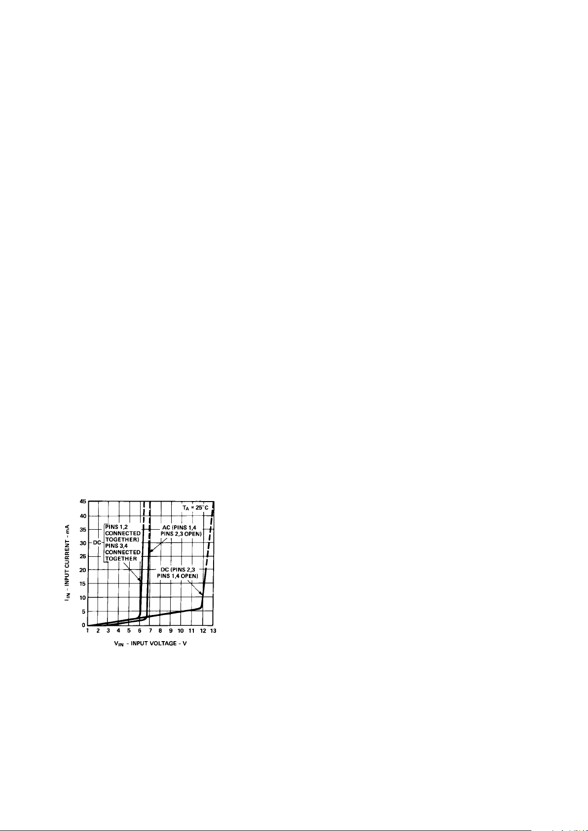
Figure 1. Typical Input Characteristics, IIN vs. VIN (AC Voltage is Instantaneous Value).
Page 9

1-356
INPUT
DEVICE TH+TH–CONNNECTION
ITHHCPL-3700 2.5 mA 1.3 mA PINS 2, 3
HCPL-3760 1.2 mA 0.6 mA OR 1, 4
V
TH(dc)
BOTH 3.7 V 2.6 V PINS 2, 3
V
TH(ac)
BOTH 4.9 V 3.7 V PINS 1, 4
Figure 3. Typical DC Threshold Levels vs. Temperature.
Figure 2. Typical Transfer Characteristics.
V
TH
– VOLTAGE THRESHOLD – V
TA – TEMPERATURE – °C
2.4
-20
4.2
04060
1.8
3.4
3.8
-40 80
2.2
2.0
20
HCPL-3700
2.6
2.8
3.0
3.2
3.6
4.0
1.4
3.2
0.8
2.4
2.8
1.2
1.0
1.6
1.8
2.0
2.2
2.6
3.0
I
TH
– CURRENT THRESHOLD – mA
I
TH+
V
TH-
I
TH-
V
TH+
V
TH
– VOLTAGE THRESHOLD – V
TA – TEMPERATURE – °C
2.4
-25
4.2
05075
1.8
3.4
3.8
-40 85
2.2
2.0
25
HCPL-3760
2.6
2.8
3.0
3.2
3.6
4.0
0.7
1.6
0.4
1.2
1.4
0.6
0.5
0.8
0.9
1.0
1.1
1.3
1.5
I
TH
– CURRENT THRESHOLD – mA
V
TH+
I
TH+
V
TH-
I
TH-
Page 10

1-357
Figure 5. Typical Input Current, IIN, and Low Level Output Voltage, VOL, vs. Temperature.
Figure 6. Typical Logic Low Supply Current vs. Supply Voltage.
I
IN
– INPUT CURRENT – mA
TA – TEMPERATURE – °C
2.4
-20
4.2
04060
1.8
3.4
3.8
-40 80
2.2
2.0
20
HCPL-3700
2.6
2.8
3.0
3.2
3.6
4.0
60
240
0
160
200
40
20
80
100
120
140
180
220
V
OL
– LOW LEVEL OUTPUT VOLTAGE – mV
V
IN
= 5.0 V
(PINS 2, 3)
V
CC
= 5.0 V
I
IN
V
CC
= 5.0 V
I
OL
= 4.2 mA
V
OL
Figure 4. Typical High Level Supply Current, I
CCH
vs.
Temperature.
I
IN
– INPUT CURRENT – mA
TA – TEMPERATURE – °C
1.2
-25
2.1
05075
0.9
1.7
1.9
-40 85
1.1
1.0
25
HCPL-3760
1.3
1.4
1.5
1.6
1.8
2.0
60
240
0
160
200
40
20
80
100
120
140
180
220
V
OL
– LOW LEVEL OUTPUT VOLTAGE – mV
V
IN
= 5.0 V
(PINS 2, 3)
V
CC
= 5.0 V
I
IN
V
CC
= 5.0 V
I
OL
= 4.2 mA
V
OL
I
CCL
– LOGIC LOW SUPPLY CURRENT – mA
VCC – SUPPLY VOLTAGE – V
2.50
2.00
6.0
4.00
8.0 12.0 14.0
0
3.00
3.50
4.0 20.018.0
1.50
1.00
0.50
10.0 16.0
HCPL-3700
I
CCL
– LOGIC LOW SUPPLY CURRENT – mA
V
CC
– SUPPLY VOLTAGE – V
1.50
6.0
3.00
8.0 12.0 14.0
0
2.00
2.50
4.0 20.018.0
1.00
0.50
10.0 16.0
HCPL-3760
I
CCH
– HIGH LEVEL SUPPLY CURRENT – µA
TA – TEMPERATURE – °C
-25
10
0
05075
10
-5
10
-1
-40 85
10
-4
25
10
-3
10
-2
V
CC
= 18 V
V
O
= OPEN
I
IN
= 0 mA
I
CCH
I
CCH
Page 11

1-358
t
p
– PROPAGATION DELAY – µs
TA – TEMPERATURE – °C
6
-202404060
0
16
20
-40 80
4
2
20
HCPL-3700
8
10
12
14
18
22
R
L
= 4.7 kΩ
C
L
= 30 pF
V
CC
= 5.0 V
V
IN
=
t
PLH
5.0 V
1 ms PULSE WIDTH
f = 100 Hz
t
r
, tf = 1 µs (10-90%)
t
PHL
Figure 7. Typical Propagation Delay vs. Temperature.
t
r
– RISE TIME – µs
TA – TEMPERATURE – °C
-206004060
0
40
50
-40 80
10
20
HCPL-3700
20
30
R
L
= 4.7 kΩ
C
L
= 30 pF
V
CC
= 5.0 V
V
IN
=
t
r
5.0 V
1 ms PULSE WIDTH
f = 100 Hz
t
r
, tf = 1 µs (10-90%)
600
0
400
500
100
200
300
t
f
– FALL TIME – ns
t
f
t
p
– PROPAGATION DELAY – µs
TA – TEMPERATURE – °C
6
-252405075
0
16
20
-40 85
4
2
25
HCPL-3760
8
10
12
14
18
22
R
L
= 4.7 kΩ
C
L
= 30 pF
V
CC
= 5.0 V
V
IN
=
t
PLH
5.0 V
1 ms PULSE WIDTH
f = 100 Hz
t
r
, tf = 1 µs (10-90%)
t
PHL
t
r
– RISE TIME – µs
TA – TEMPERATURE – °C
-253005075
0
20
25
-40 85
5
25
HCPL-3760
10
15
R
L
= 4.7 kΩ
C
L
= 30 pF
V
CC
= 5.0 V
V
IN
=
t
f
5.0 V
1 ms PULSE WIDTH
f = 100 Hz
tr, tf = 1 µs (10-90%)
t
r
t
f
– FALL TIME – ns
700
100
500
600
200
300
400
Figure 8. Typical Rise, Fall Times vs. Temperature.
Figure 9. Common Mode Transient Immunity
vs. Common Mode Transient Amplitude.
CM – COMMON MODE TRANSIENT IMMUNITY – V/ µs
VCM – COMMON MODE TRANSIENT AMPLITUDE – V
400
5000
800 1600
0
3000
4000
0 2000
500
1200
1000
2000
V
CC
= 5.0 V
I
IN
= 3.11 mA (3700)
I
IN
= 1.53 mA (3760)
V
OL
= 0.8 V
R
L
= 4.7 kΩ
T
A
= 25 °C
V
CC
= 5.0 V
I
IN
= 0 mA
V
OH
= 2.0 V
R
L
= 4.7 kΩ
T
A
= 25 °C
CM
L
CM
H
Page 12
1-359
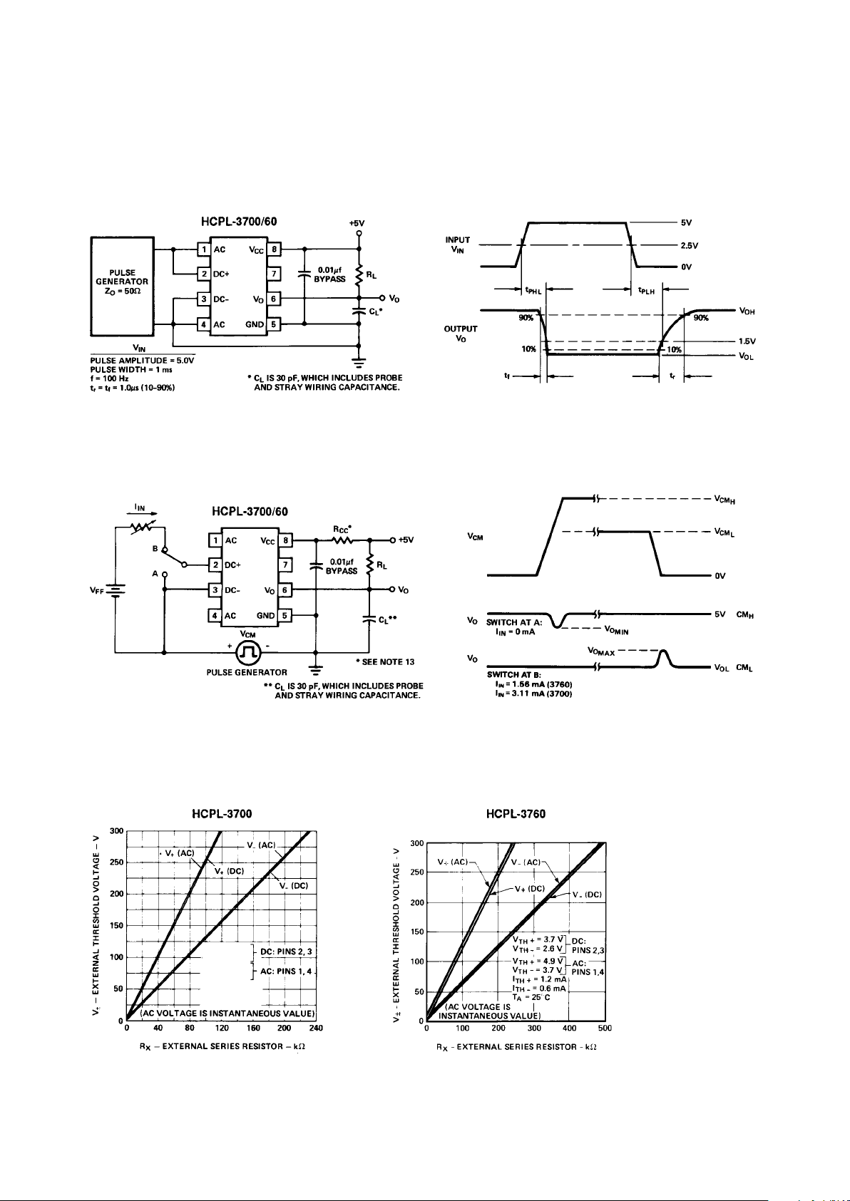
Figure 12. Typical External Threshold Characteristics, V ± vs. R
X
.
Figure 10. Switching Test Circuit.
Figure 11. Test Circuit for Common Mode Transient Immunity and Typical Waveforms.
V
TH+
= 3.7 V
V
TH–
= 2.6 V
V
TH+
= 4.9 V
V
TH–
= 3.7 V
I
TH+
= 2.5 mA
I
TH–
= 1.3 mA
T
A
= 25 °C
Page 13

1-360
Electrical Considerations
The HCPL-3700/3760 optocouplers have internal temperature
compensated, predictable voltage
and current threshold points
which allow selection of an
external resistor, RX, to determine
larger external threshold voltage
levels. For a desired external
threshold voltage, V±, a corresponding typical value of RX can
be obtained from Figure 12.
Specific calculation of RX can be
obtained from Equation (1).
Specification of both V+ and V
-
voltage threshold levels simultaneously can be obtained by the
use of RX and RP as shown in
Figure 13 and determined by
Equations (2) and (3).
RX can provide over-current
transient protection by limiting
input current during a transient
condition. For monitoring contacts of a relay or switch, the
HCPL-3700/3760 in combination
with RX and RP can be used to
allow a specific current to be
conducted through the contacts
for cleaning purposes (wetting
current).
The choice of which input voltage
clamp level to choose depends
upon the application of this
device (see Figure 1). It is recommended that the low clamp
condition be used when possible.
The low clamp condition in
conjunction with the low input
current feature will ensure
extremely low input power
dissipation.
In applications where dVCM/dt
may be extremely large (such as
static discharge), a series resistor,
RCC, should be connected in
series with VCC and Pin 8 to protect the detector IC from destructively high surge currents. See
Note 13 for determination of RCC.
In addition, it is recommended
that a ceramic disc bypass
capacitor of 0.01 µF be placed
between Pins 8 and 5 to reduce
the effect of power supply noise.
For interfacing ac signals to TTL
systems, output low pass filtering
can be performed with a pullup
resistor of 1.5 kΩ and 20 µF
capacitor. This application
requires a Schmitt trigger gate to
avoid slow rise time chatter
problems. For ac input applications, a filter capacitor can be
placed across the dc input
terminals for either signal or
transient filtering.
Either ac (Pins 1, 4) or dc
(Pins 2, 3) input can be used to
determine external threshold
levels.
V+ - V
TH+
(-) (-)
RX = (1)
I
TH+
(-)
For two specifically selected
external threshold voltage levels,
V+ and V-, the use of RX and R
P
will permit this selection via
equations (2), (3) provided the
following conditions are met. If
the denominator of equation (2)
is positive, then
V
+
V
TH+
V+ - V
TH+ITH+
≥ and <
V
-
V
TH-
V- - V
TH-
I
TH-
Conversely, if the denominator of
equation (2) is negative, then
V
+
V
TH+
V+ - V
TH+ITH+
≤ and >
V
-
V
TH-
V- - V
TH-
I
TH-
V
TH-
(V+) - V
TH+
(V-)
RX = (2)
I
TH+
(V
TH-
) - I
TH-
(V
TH+
)
V
TH-
(V+) - V
TH+
(V-)
RP = (3)
I
TH+(V--VTH-
)+I
TH-(VTH+-V+
)
Figure 13. External Threshold Voltage Level Selection.
For one specifically selected
external threshold voltage level
V+ or V-, RX can be determined
without use of RP via
 Loading...