

Page 1
1-288
H
8 MBd Low Input Current
Optocoupler
Technical Data
HCPL-2300
Features
• Guaranteed Low Thresholds:
IF = 0.5 mA, V
F
≤1.5 V
• High Speed: Guaranteed
5 MBd over Temperature
• Versatile: Compatible with
TTL, LSTTL and CMOS
• Efficient 820 nm AlGaAs
LED
• Internal Shield for
Guaranteed Common Mode
Rejection
• Schottky Clamped, Open
Collector Output with
Optional Integrated Pull-Up
Resistor
• Static and Dynamic
Performance Guaranteed
from -40°C to 85°C
• Safety Approval
UL Recognized -2500 V rms for
1 minute
CSA Approved
VDE 0884 Approved with
V
IORM
= 630 V peak
(Option 060)
Applications
• Ground Loop Elimination
• Computer-Peripheral
Interfaces
• Level Shifting
• Microprocessor System
Interfaces
• Digital Isolation for A/D,
D/A Conversion
• RS-232-C Interface
• High Speed, Long Distance
Isolated Line Receiver
Description
The HCPL-2300 optocoupler
combines an 820 nm AlGaAs
photon emitting diode with an
integrated high gain photon
detector. This combination of
Hewlett-Packard designed and
manufactured semiconductor
devices brings new high
performance capabilities to
designers of isolated logic and
data communication circuits.
The new low current, high speed
AlGaAs emitter manufactured
with a unique diffused junction,
has the virtue of fast rise and fall
times at low drive currents.
Figure 6 illustrates the propagation delay vs. input current
characteristic. These unique
CAUTION: It is advised that normal static precautions be taken in handling and assembly of this component to
prevent damage and/or degradation which may be induced by ESD.
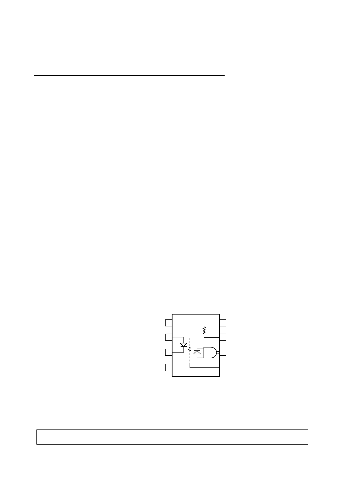
Functional Diagram
A 0.1 pF bypass capacitor must be connected between pins 5 and 8.
8
7
6
1
3
5
2
4
NC
ANODE
CATHODE
NC
V
CC
R
L
V
OUT
GND
5965-3587E
Page 2
1-289
Ordering Information
Specify part number followed by Option Number (if desired).
HCPL-2300# XXX
060 = VDE 0884 V
IORM
= 630 V peak Option
300 = Gull Wing Surface Mount Lead Option
500 = Tape/Reel Package Option (1 K min)
Option data sheets available. Contact your Hewlett-Packard sales representative or authorized distributor for
information.
characteristics enable this device
to be used in an RS-232-C interface with ground loop isolation
and improved common mode
rejection. As a line receiver, the
HCPL-2300 will operate over
longer line lengths for a given
data rate because of lower IF and
VF specifications.
The output of the shielded integrated detector circuit is an open
collector Schottky clamped transistor. The shield, which shunts
capacitively coupled common
mode noise to ground, provides a
guaranteed transient immunity
specification of 100 V/µs. The
output circuit includes an
optional integrated 1000 Ω pullup resistor for the open collector.
This gives designers the flexibility
to use the internal resistor for
pull-up to five volt logic or to use
an external resistor for connection to supply voltages up to 18 V
(CMOS logic voltage).
The Electrical and Switching
Characteristics of the HCPL-2300
are guaranteed over a temperature range of -40°C to 85°C. This
enables the user to confidently
design a circuit which will
operate under a broad range of
operating conditions.
Schematic
I
F
SHIELD
V
F
V
CC
GND
I
CC
+
–
2
3
8
5
V
O
7
6
A 0.1 µF CAPACITOR MUST
BE CONNECTED BETWEEN
PINS 8 AND 5 (SEE NOTE 1).
TRUTH TABLE
(POSITIVE LOGIC)
LED
ON
OFF
OUTPUT
L
H
R
L
1000 Ω
Page 3
1-290
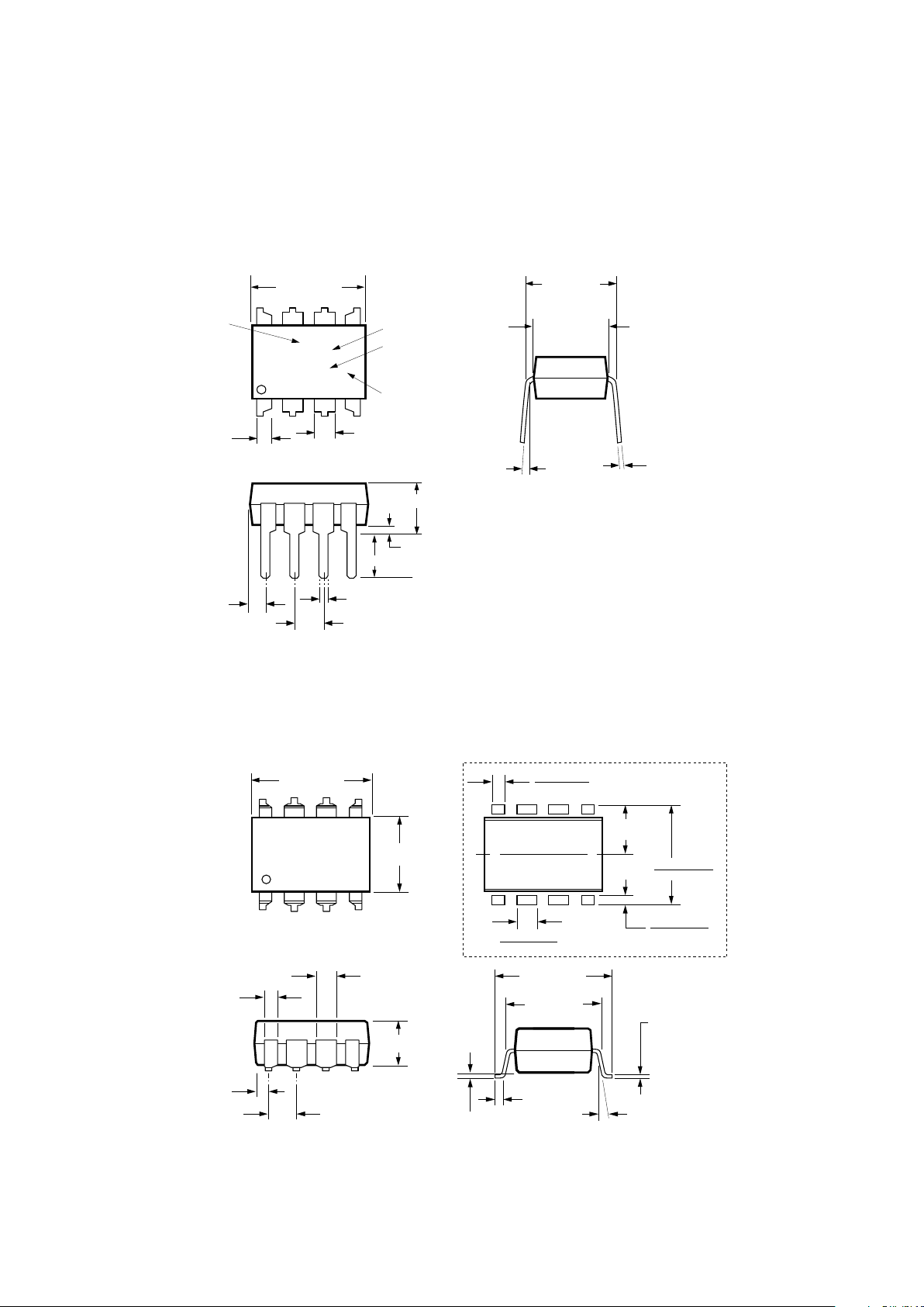
Package Outline Drawings
8-Pin DIP Package (HCPL-2300)
8-Pin DIP Package with Gull Wing Surface Mount Option 300 (HCPL-2300)
0.635 ± 0.25
(0.025 ± 0.010)
12° NOM.
9.65 ± 0.25
(0.380 ± 0.010)
0.635 ± 0.130
(0.025 ± 0.005)
7.62 ± 0.25
(0.300 ± 0.010)
5
6
7
8
4
3
2
1
9.65 ± 0.25
(0.380 ± 0.010)
6.350 ± 0.25
(0.250 ± 0.010)
1.016 (0.040)
1.194 (0.047)
1.194 (0.047)
1.778 (0.070)
9.398 (0.370)
9.906 (0.390)
4.826
(0.190)
TYP.
0.381 (0.015)
0.635 (0.025)
PAD LOCATION (FOR REFERENCE ONLY)
1.080 ± 0.320
(0.043 ± 0.013)
4.19
(0.165)
MAX.
1.780
(0.070)
MAX.
1.19
(0.047)
MAX.
2.54
(0.100)
BSC
DIMENSIONS IN MILLIMETERS (INCHES).
LEAD COPLANARITY = 0.10 mm (0.004 INCHES).
0.254
+ 0.076
- 0.051
(0.010
+ 0.003)
- 0.002)
9.65 ± 0.25
(0.380 ± 0.010)
1.78 (0.070) MAX.
1.19 (0.047) MAX.
HP XXXXZ
YYWW
DATE CODE
1.080 ± 0.320
(0.043 ± 0.013)
2.54 ± 0.25
(0.100 ± 0.010)
0.51 (0.020) MIN.
0.65 (0.025) MAX.
4.70 (0.185) MAX.
2.92 (0.115) MIN.
DIMENSIONS IN MILLIMETERS AND (INCHES).
5678
4321
5° TYP.
OPTION CODE*
UL
RECOGNITION
UR
0.254
+ 0.076
- 0.051
(0.010
+ 0.003)
- 0.002)
7.62 ± 0.25
(0.300 ± 0.010)
6.35 ± 0.25
(0.250 ± 0.010)
TYPE NUMBER
* MARKING CODE LETTER FOR OPTION NUMBERS.
"V" = OPTION 060
OPTION NUMBERS 300 AND 500 NOT MARKED.
Page 4
1-291
Insulation and Safety Related Specifications
Parameter Symbol Value Units Conditions
Min. External Air Gap L(IO1) 7.1 mm Measured from input terminals to output
(External Clearance) terminals, shortest distance through air
Min. External Tracking Path L(IO2) 7.4 mm Measured from input terminals to output
(External Creepage) terminals, shortest distance path along body
Min. Internal Plastic Gap 0.08 mm Through insulation distance, conductor to
(Internal Clearance) conductor, usually the direct distance
between the photoemitter and photodetector
inside the optocoupler cavity
Tracking Resistance CTI 200 Volts DIN IEC 112/VDE 0303 PART 1
(Comparative Tracking Index)
Isolation Group IIIa Material Group (DIN VDE 0110, 1/89, Table 1)
Option 300 – surface mount classification is Class A in accordance with CECC 00802.
Regulatory Information
The HCPL-2300 has been
approved by the following
organizations:
UL
Recognized under UL 1577,
Component Recognition
Program, File E55361.
CSA
Approved under CSA Component
Acceptance Notice #5, File CA
88324.
VDE
Approved according to VDE
0884/06.92 (Option 060 only)
Figure 1. Maximum Solder Reflow Thermal Profile.
(Note: Use of non-chlorine activated fluxes is recommended.)
240
∆T = 115°C, 0.3°C/SEC
0
∆T = 100°C, 1.5°C/SEC
∆T = 145°C, 1°C/SEC
TIME – MINUTES
TEMPERATURE – °C
220
200
180
160
140
120
100
80
60
40
20
0
260
123456789101112
Thermal Profile (Option #300)
Page 5

1-292
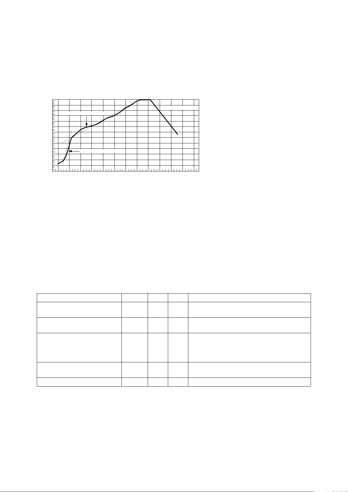
VDE 0884 Insulation Related Characteristics (HCPL-2300 Option 060 ONLY)
Description Symbol Characteristic Units
Installation classification per DIN VDE 0110/1.89, Table 1
for rated mains voltage ≤ 300 V rms I-IV
for rated mains voltage ≤ 450 V rms I-III
Climatic Classification 55/85/21
Pollution Degree (DIN VDE 0110/1.89) 2
Maximum Working Insulation Voltage V
IORM
630 V peak
Input to Output Test Voltage, Method b*
V
IORM
x 1.875 = VPR, 100% Production Test with tm = 1 sec, V
PR
1181 V peak
Partial Discharge < 5 pC
Input to Output Test Voltage, Method a*
V
IORM
x 1.5 = VPR, Type and sample test, tm = 60 sec, V
PR
945 V peak
Partial Discharge < 5 pC
Highest Allowable Overvoltage*
(Transient Overvoltage, t
ini
= 10 sec) V
IOTM
6000 V peak
Safety Limiting Values
(Maximum values allowed in the event of a failure,
also see Figure 11, Thermal Derating curve.)
Case Temperature T
S
175 °C
Input Current I
S,INPUT
230 mA
Output Power P
S,OUTPUT
600 mW
Insulation Resistance at TS, VIO = 500 V R
S
≥ 10
9
Ω
*Refer to the front of the optocoupler section of the current catalog, under Product Safety Regulations section, (VDE 0884), for a
detailed description.
Note: Isolation characteristics are guaranteed only within the safety maximum ratings which must be ensured by protective circuits in
application.
Recommended Operating Conditions
Parameter Symbol Min. Max. Units
Input Voltage, Low Level V
FL
-2.5 0.8 V
Input Current High Level 0°C to 85°CIFH0.5 1.0 mA
-40°C to 85°C 0.5 0.75
Supply Voltage, Output V
CC
4.75 5.25 V
Fan Out (TTL Load) N 5
Operating Temperature T
A
-40 85 °C
Absolute Maximum Ratings
(No Derating Required up to 55°C)
Storage Temperature, TS............................................. -55°C to +125°C
Operating Temperature, TA........................................... -40°C to +85°C
Lead Solder Temperature, max .......................................... 260°C for 10 s
(1.6 mm below seating plane)
Average Forward Input Current - IF............................................ 5 mA
[2]
Reverse Input Voltage, VR..............................................................3.0 V
Supply Voltage, VCC............................................................... 0 V to 7.0 V
Pull-Up Resistor Voltage, VRL............................................. - 0.5 V to V
CC
Output Collector Current, IO............................................ -25 to 25 mA
Input Power Dissipation, PI........................................................10 mW
Output Collector Power Dissipation, PO.....................................40 mW
Output Collector Voltage, VO........................................... -0.5 V to 18 V
Infrared and Vapor Phase Reflow Temperature
(Option #300) ..........................................see Fig. 1, Thermal Profile
Page 6

1-293
DC Electrical Specifications
For -40°C ≤ TA ≤ 85°C, 4.75 V ≤ VCC ≤ 5.25 V, VFL ≤ 0.8 V, unless otherwise specified.
All typicals at TA = 25°C and VCC = 5 V , unless otherwise specified. See note 1.
Parameter Symbol Min. Typ. Max. Units Test Conditions Fig. Note
High Level Output I
OH
0.05 250 µAVF = 0.8 V, VO = 18 V 4
Current
Low Level Output V
OL
0.4 0.5 V IF = 0.5 mA 3
Voltage IOL (Sinking) = 8 mA
High Level Supply I
CCH
4.0 6.3 mA IF = 0 mA, VCC = 5.25 V
Current
Low Level Supply Current I
CCL
6.2 10.0 mA IF = 1.0 mA, VCC = 5.25 V
Input Forward Voltage V
F
1.0 1.3 1.5 V TA = 25°CIF = 1.0 mA 2
0.85 1.65
Input Diode Temperature ∆V
F
-1.6 mV/°CIF = 1.0 mA
Coefficient
Input Reverse BV
R
3.0 V IR = 10 µA
Breakdown Voltage
Input Capacitance C
IN
18 pF VF = 0 V, f = 1 MHz
Internal Pull-up Resistor R
L
680 1000 1700 Ω TA = 25°C
∆T
A
Switching Specifications
For -40°C ≤ TA ≤ 85°C, 0.5 mA ≤ IFH ≤ 0.75 mA;
For 0°C ≤ TA ≤ 85°C, 0.5 mA ≤ IFH ≤ 1.0 mA; With 4.75 V ≤ VCC ≤ 5.25 V, VFL ≤ 0.8 V, unless otherwise
specified. All typicals at TA = 25°C and VCC = 5 V, IFH = 0.625 mA, unless otherwise specified. See note 1.
Parameter Symbol Min. Typ. Max. Units Test Conditions Fig. Note
Propagation Delay Time t
PLH
95 ns CP = 0 pF 5, 6, 8 4, 8
85 160 CP = 20 pF 5, 8
Propagation Delay Time t
PHL
110 ns CP = 0 pF 5, 6, 8 5, 8
35 200 CP = 20 pF 5, 8
Output Rise Time (10-90%) t
r
40 ns CP = 20 pF 7, 8 8
Output Fall Time (90-10%) t
f
20 ns
Common Mode Transient |CMH| 100 400 V/µsVCM = 50 V (peak), 9, 10 6
Immunity at High VO (min.) = 2 V,
Output Level RL = 560 Ω,
IF = 0 mA
Common Mode Transient |CML| 100 400 V/µsVCM = 50 V (peak), 9, 10 7
Immunity at Low VO (max.) = 0.8 V,
Output Level RL = 560 Ω,
IF = 0.5 mA
to Logic High Output Level
to Logic Low Output Level
Page 7

1-294
Notes:
1. Bypassing the power supply line is
required with a 0.1 µF ceramic disc
capacitor adjacent to each optocoupler
as illustrated in Figure 19. The power
supply bus for the optocoupler(s)
should be separate from the bus for
any active loads, otherwise a larger
value of bypass capacitor (up to
0.5 µF) may be needed to suppress
regenerative feedback via the power
supply.
2. Peaking circuits may produce transient
input currents up to 100 mA, 500 ns
maximum pulse width, provided
average current does not exceed 5 mA.
Package Characteristics
For -40°C ≤ TA ≤ 85°C, unless otherwise specified. All typicals at TA = 25°C.
Parameter Symbol Min. Typ. Max. Units Test Conditions Fig. Notes
Input-Output Momentary V
ISO
2500 V rms RH ≤ 50%, t = 1 min, 3, 9
Withstand Voltage* TA = 25°C
Resistance, Input-Output R
I-O
10
12
Ω V
I-O
= 500 V 3
Capacitance, Input-Output C
I-O
0.6 pF f = 1 MHz 3
*The Input-Output Momentary Withstand Voltage is a dielectric voltage rating that should not be interpreted as an input-output
continuous voltage rating. For the continuous voltage rating refer to the VDE 0884 Insulation Characteristics Table (if applicable),
your equipment level safety specification, or HP Application Note 1074, “Optocoupler Input-Output Endurance Voltage.”
7. CML is the maximum tolerable rate of
fall of the common mode voltage to
assure that the output will remain in a
low logic state (i.e., V
OUT
< 0.8 V).
8. CP is the peaking capacitance. Refer to
test circuit in Figure 8.
9. In accordance with UL 1577, each
optocoupler is momentary withstand
proof tested by applying an insulation
test voltage ≥ 3000 Vrms for 1 second
(leakage detection current limit,
I
I-O
≤ 5 µA). This test is performed
before the 100% production test for
partial discharge (Method b) shown in
the VDE 0884 Insulation Characteristics Table, if applicable.
3. Device considered a two terminal
device: pins 1, 2, 3, and 4 shorted
together, and pins 5, 6, 7, and 8
shorted together.
4. The t
PLH
propagation delay is
measured from the 50% point on the
trailing edge of the input pulse to the
1.5 V point on the trailing edge of the
output pulse.
5. The t
PHL
propagation delay is
measured from the 50% point on the
leading edge of the input pulse to the
1.5 V point on the leading edge of the
output pulse.
6. CMH is the maximum tolerable rate of
rise of the common mode voltage to
assure that the output will remain in a
high logic state (i.e., V
OUT
> 2.0 V).
Figure 3. Typical Output Voltage vs.
Forward Input Current vs.
Temperature.
Figure 2. Typical Input Diode
Forward Characteristics.
Figure 4. Typical Logic High Output
Current vs. Temperature.
Page 8

1-295
Figure 5. Typical Propagation Delay
vs. Temperature and Forward
Current with and without Application
of a Peaking Capacitor.
Figure 6. Typical Propagation Delay
vs. Forward Current.
Figure 7. Typical Rise, Fall Time vs.
Temperature.
Figure 8. Test Circuit for t
PHL
, t
PLH
, tr, and tf. Figure 9. Typical Common Mode
Transient Immunity vs. Common
Mode Transient Amplitude.
Page 9

1-296
Applications
The HCPL-2300 optocoupler has
the unique combination of low
0.5 mA LED operating drive
current at a 5 MBd speed
performance. Low power supply
current requirement of 10 mA
maximum at 5.25 V and the
ability to provide isolation
between logic systems fulfills
numerous applications ranging
from logic level translations, line
receiver and party line receiver
applications, microprocessor I/O
port isolation, etc. The open collector output allows for wired-OR
arrangement. Specific interface
circuits are illustrated in Figures
12-16, and 18 with corresponding component values, performance data and recommended
layout in Figures 17 and 19.
For -40°C to 85°C operating
temperature range, a mid-range
LED forward current (IF) of
0.625 mA is recommended in
order to prevent overdriving the
integrated circuit detector due to
increased LED efficiency at
temperatures between 0°C and
-40°C. For narrower temperature
range of 0°C to 85°C, a suggested
operating LED current of
0.75 mA is recommended for the
mid-range operating point and for
minimal propagation delay skew.
A peaking capacitance of 20 pF
in parallel with the current
limiting resistor for the LED
shortens t
PHL
by approximately
33% and t
PLH
by 13%. Maintaining LED forward voltage (VF)
below 0.8 V will guarantee that
the HCPL-2300 output is off.
The recommended shunt drive
technique for TTL/LSTTL/CMOS
of Figure 12 provides for optimal
speed performance, no leakage
current path through the LED,
and reduced common mode
influences associated with series
switching of a “floating” LED.
Alternate series drive techniques
with either an active CMOS
inverter or an open collector TTL/
LSTTL inverter are illustrated in
Figures 13 and 14 respectively.
Open collector leakage current of
250 µA has been compensated by
the 3.16 KΩ resistor (Figure 14)
at the expense of twice the
operating forward current.
An application of the HCPL-2300
as an unbalanced line receiver for
use in long line twisted wire pair
communication links is shown in
Figure 15. Low LED IF and V
F
allow longer line length, higher
speed and multiple stations on
the line in comparison to higher
IF, VF optocouplers. Greater
speed performance along with
nearly infinite common mode
immunity are achieved via the
balanced split phase circuit of
Figure 16. Basic balanced
differential line receiver can be
accomplished with one HCPL2300 in Figure 16, but with a
typical 400 V/µs common mode
immunity. Data rate versus
distance for both the above
unbalanced and balanced line
receiver applications are compared in Figure 17. The RS-232-C
interface circuit of Figure 18
Figure 10. Test Circuit for Common Mode Transient Immunity and Typical Waveforms.
Figure 11. Thermal Derating Curve,
Dependence of Safety Limiting Value
with Case Temperature per
VDE 0884.
OUTPUT POWER – P
S
, INPUT CURRENT – I
S
0
0
TS – CASE TEMPERATURE – °C
20050
400
12525 75 100 150
600
800
200
100
300
500
700
PS (mW)
I
S
(mA)
175
Page 10

1-297
Figure 14. Series Drive from Open Collector TTL/LSTTL
Units.
Figure 13. Active CMOS Series Drive Circuit.
Figure 12. Recommended Shunt Drive Circuit for Interfacing between TTL/LSTTL/CMOS Logic Systems.
provides guaranteed minimum
common mode immunity of
100 V/µs while maintaining the
2:1 dynamic range of IF.
A recommended layout for use
with an internal 1000 Ω resistor
or an external pull-up resistor
and required VCC bypass capacitor is given in Figure 19. V
CC1
is
used with an external pull-up
resistor for output voltage levels
(VO) greater than or equal to 5 V.
As illustrated in Figure 19, an
optional VCC and GND trace can
be located between the input and
the output leads of the HCPL2300 to provide additional noise
immunity at the compromise of
insulation capability (V
I-O
).
Page 11

1-298
Figure 15. Application of HCPL-2300 as Isolated, Unbalanced Line Receiver(s).
Figure 16. Application of Two HCPL-2300 Units Operating as an Isolated, High Speed, Balanced, Split Phase Line
Receiver with Significantly Enhanced Common Mode Immunity.
REFERENCE FIGURE 17 FOR DATA RATE vs. LINE DISTANCE L.
REFERENCE FIGURE 17 FOR DATA RATE vs. LINE DISTANCE L.
Page 12

1-299
Figure 19. Recommended Printed Circuit Board Layout.
Figure 18. RS-232-C Interface Circuit with HCPL-2300.
0°C < TA < 85°C.
Figure 17. Typical Point to Point Data Rate vs. Length of
Line for Unbalanced (Figure 15) and Balanced (Figure 16)
Line Receivers Using HCPL-2300 Optocouplers.
RS-232-C
SIGNAL
3 V – 25 V
-3 V – -25 V
(FIGURE 16)
(FIGURE 15)
 Loading...