

Page 1
HA-5340
Data Sheet September 1998 File Number 2859.3
700ns, Low Distortion, Precision Sample
and Hold Amplifier
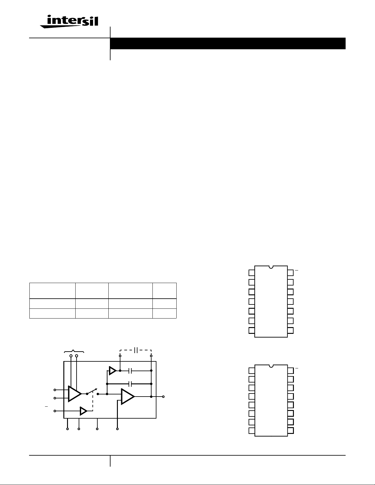
The HA-5340 combines the advantages of two sample/ hold
architectures to create a new generation of monolithic
sample/hold. High amplitude, high frequency signals can be
sampled with very low distortion being introduced. The
combination of exceptionally fast acquisition time and
specified/characterized hold mode distortion is an industry
first. Additionally, the AC performance is only minimally
affected by additional hold capacitance.
To achieve this level of performance, the benefits of an
integrating output stage have been combined with the
advantages of a buff ered hold capacitor. To the user this
translates to a front-endstagethat has high bandwidth due to
charging only a small capacitive load and an output stage with
constant pedestal error which can be nulled out using the
offset adjust pins. Since the performance penalty for
additional hold capacitance is low , the designer can further
minimize pedestal error and droop rate without sacrificing
speed.
Low distortion, fast acquisition, and low droop rate are the
result, making the HA-5340 the obvious choice for high
speed, high accuracy sampling systems. For a Military
temperature range version request the HA-5340/883 data
sheet.
Ordering Information
TEMP.
PART NUMBER
RANGE (oC) PACKAGE
HA3-5340-5 0 to 75 14 Ld PDIP E14.3
HA9P5340-5 0 to 75 16 Ld SOIC M16.3
PKG.
NO.
Functional Diagram
C
HOLD EXTERNAL
(OPTIONAL)
11
6
SIGNAL GND
C
HOLD
120pF
C
COMP
15pF
7
OUT
-IN
+IN
S/H
CONTROL
ADJUST OFFSET
437
1
2
14
95 13
V+
SUPPLYV-
GND
Features
• Fast Acquisition Time (0.01%) . . . . . . . . . . . . . . . . .700ns
• Fast Hold Mode Settling Time (0.01%). . . . . . . . . . . .200n
• Low Distortion (Hold Mode) . . . . . . . . . . . . . . . . . . -72dBc
(VIN = 200kHz, fS = 450kHz, 5V
• Bandwidth Minimally Affected By External C
P-P
)
H
• Fully Differential Analog Inputs
• Built-In 135pF Hold Capacitor
• Pin Compatible with HA-5320
Applications
• High Bandwidth Precision Data Acquisition Systems
• Inertial Navigation and Guidance Systems
• Ultrasonics
• SONAR
• RADAR
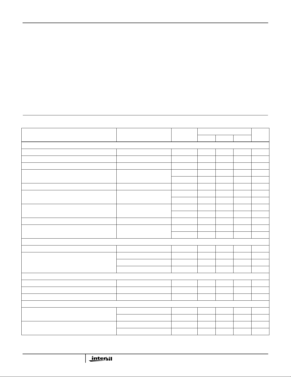
Pinouts
HA-5340
(PDIP)
TOP VIEW
-IN
+IN
OFFSET ADJ.
OFFSET ADJ.
SIG. GND
OUTPUT
-IN
+IN
OFFSET ADJ.
OFFSET ADJ.
NC
SIG. GND
OUTPUT
V-
V-
1
2
3
4
5
6
7
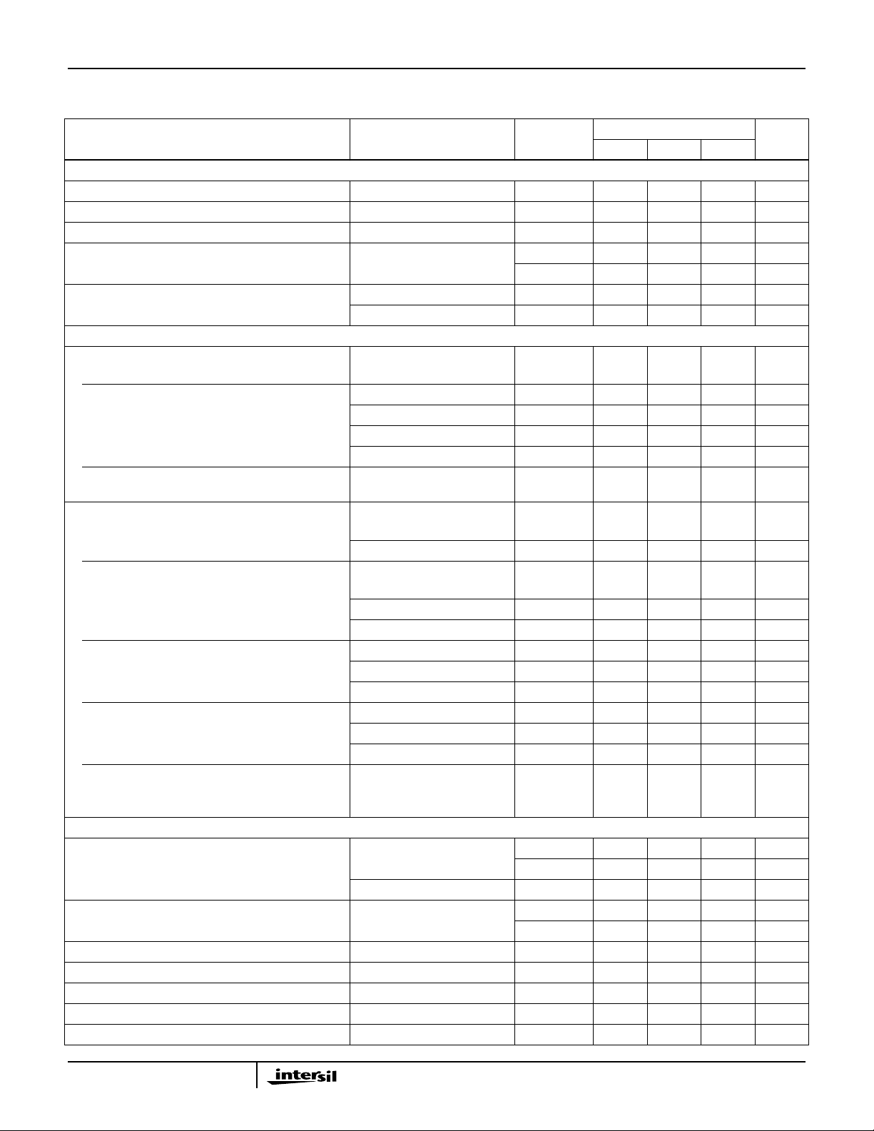
HA-5340
(SOIC)
TOP VIEW
1
2
3
4
5
6
7
8
S/H CONTROL
14
13
SUPPLY GND
12
NC
EXTERNAL
11
HOLD CAP.
10
NC
9
V+
8
NC
16
S/H CONTROL
SUPPLY GND
15
NC
14
NC
13
EXTERNAL
12
HOLD CAP.
NC
11
NC
10
V+
9
1
CAUTION: These devices are sensitive to electrostatic discharge; follow proper IC Handling Procedures.
1-888-INTERSIL or 321-724-7143
| Copyright © Intersil Corporation 1999
Page 2
HA-5340
Absolute Maximum Ratings Thermal Information
Voltage Between V+ and V- Terminals. . . . . . . . . . . . . . . . . . . . 36V
Differential Input Voltage . . . . . . . . . . . . . . . . . . . . . . . . . . . . . . 24V
Digital Input Voltage. . . . . . . . . . . . . . . . . . . . . . . . . . . . . . +8V, -6V
Output Current, Continuous. . . . . . . . . . . . . . . . . . . . . . . . . . ±20mA
Operating Conditions
Temperature Range
HA-5340-5 . . . . . . . . . . . . . . . . . . . . . . . . . . . . . . . . 0oC to 75oC
Supply Voltage Range (Typical). . . . . . . . . . . . . . . . . ±12V to ±18V
CAUTION: Stresses above those listed in “Absolute Maximum Ratings” may cause permanent damage to the device. This is a stress only rating and operation of the
device at these or any other conditions above those indicated in the operational sections of this specification is not implied.
NOTES:
1. Maximum power dissipation must be designed to maintain the junction temperature below 150oC for the plastic packages.
2. θJA is measured with the component mounted on an evaluation PC board in free air.
Thermal Resistance (Typical, Note 2) θJA (oC/W) θJC (oC/W)
PDIP Package . . . . . . . . . . . . . . . . . . . 90 N/A
SOIC Package . . . . . . . . . . . . . . . . . . . 95 N/A
Maximum Junction Temperature (Plastic Package, Note 1) . .150oC
Maximum Storage Temperature Range. . . . . . . . . . -65oC to 150oC
Maximum Lead Temperature (Soldering 10s) . . . . . . . . . . . . 300oC
(SOIC - Lead Tips Only)
Electrical Specifications V
Gain Configuration (Output tied to -Input), R
PARAMETER TEST CONDITIONS TEMP. (
INPUT CHARACTERISTICS
Input Voltage Range Full -10 - +10 V
Input Resistance (Note 3) 25 - 1 - MΩ
Input Capacitance 25 - - 3 pF
Input Offset Voltage 25 - - 1.5 mV
Offset Voltage Temperature Coefficient Full - - 30 µV/oC
Bias Current 25 - ±70 - nA
Offset Current 25 - ±50 - nA
Common Mode Range Full -10 - +10 V
CMRR ±10V, Note 4 25 - 83 - dB
TRANSFER CHARACTERISTICS
Gain DC 25 110 140 - dB
Gain Bandwidth Product CH External = 0pF Full - 10 - MHz
TRANSIENT RESPONSE
Rise Time 200mV Step 25 - 20 30 ns
Overshoot 200mV Step 25 - 35 50 %
Slew Rate 10V Step 25 40 60 - V/µs
DIGITAL INPUT CHARACTERISTICS
Input Voltage V
Input Current VIL = 0V Full - 7 40 µA
= ±15.0V; CH = Internal = 135pF; Digital Input: VIL = +0.8V (Sample), VIH = +2.0V (Hold). Non-Inverting Unity
SUPPLY
CH External = 100pF Full - 9.6 - MHz
CH External = 1000pF Full - 6.7 - MHz
IH
V
IL
VIH = 5V Full - 4 40 µA
= 2kΩ, CL = 60pF, Unless Otherwise Specified
L
o
C)
Full - - 3.0 mV
Full - - ±350 nA
Full - - ±350 nA
Full 72 - - dB
Full 2.0 - - V
Full - - 0.8 V
HA-5340-5
UNITSMIN TYP MAX
2
Page 3
HA-5340
Electrical Specifications V
= ±15.0V; CH = Internal = 135pF; Digital Input: VIL = +0.8V (Sample), VIH = +2.0V (Hold). Non-Inverting Unity
SUPPLY
Gain Configuration (Output tied to -Input), RL = 2kΩ, CL = 60pF, Unless Otherwise Specified (Continued)
HA-5340-5
PARAMETER TEST CONDITIONS TEMP. (
o
C)
UNITSMIN TYP MAX
OUTPUT CHARACTERISTICS
Output Voltage Full -10 - +10 V
Output Current Full -10 - +10 mA
Full Power Bandwidth (Note 5) Full 0.6 0.9 - MHz
Output Resistance Hold Mode 25 - 0.05 0.1 Ω
Full - 0.07 0.15 Ω
Total Output Noise
DC to 10MHz
Sample Mode 25 - 325 400 µV
Hold Mode 25 - 325 400 µV
DISTORTION CHARACTERISTICS
SAMPLE MODE
Signal to Noise Ratio (RMS Signal to RMS Noise) V
= 200kHz, 20V
IN
Total Harmonic Distortion VIN = 200kHz, 5V
VIN = 200kHz, 10V
VIN = 200kHz, 20V
VIN = 500kHz, 5V
Intermodulation Distortion VIN = 10V
, f1 = 20kHz,
P-P
P-P
P-P
P-P
P-P
P-P
Full - 115 - dB
Full -90 -100 - dBc
Full -76 -82 - dBc
Full -70 -74 - dBc
Full -66 -75 - dBc
Full -78 -83 - dBc
f2 = 21kHz
HOLD MODE (50% Duty Cycle S/H)
Signal to Noise Ratio
(RMS Signal to RMS Noise) f
= 450kHz
S
VIN = 200kHz, 5V
VIN = 200kHz, 10V
P-P
P-P
25 - 76 - dB
25 - 76 - dB
Total Harmonic Distortion
= 450kHz VIN = 200kHz, 5V
f
S
VIN = 200kHz, 10V
VIN = 200kHz, 20V
fS = 450kHz VIN = 100kHz, 5V
VIN = 100kHz, 10V
VIN = 100kHz, 20V
fS = 2fIN(Nyquist) VIN = 20kHz, 5V
VIN = 50kHz, 5V
VIN = 100kHz, 5V
P-P
P-P
P-P
P-P
P-P
P-P
P-P
P-P
P-P
25 - -72 - dBc
25 - -66 - dBc
25 - -56 - dBc
25 - -84 - dBc
25 - -71 - dBc
25 - -61 - dBc
25 - -95 - dBc
25 - -91 - dBc
25 - -82 - dBc
Intermodulation Distortion
= 450kHz VIN = 10V
f
S
P-P
25 - -79 - dBc
(f1 = 20kHz, f2 = 21kHz)
SAMPLE AND HOLD CHARACTERISTICS
Acquisition Time 10V Step to 0.01% 25 - 700 - ns
Full - - 900 ns
10V Step to 0.1% 25 - 430 600 ns
Droop Rate CH = Internal 25 - 0.1 - µV/µs
Full - - 95 µV/µs
Hold Step Error VIL = 0V, VIH = 4.0V, tR = 5ns 25 - 15 - mV
Hold Mode Settling Time To ±1mV Full - 200 300 ns
Hold Mode Feedthrough 20V
, 200kHz, Sine Full - -76 - dB
P-P
EADT (Effective Aperture Delay Time) 25 - -15 - ns
Aperture Uncertainty 25 - 0.2 - ns
RMS
RMS
3
Page 4

HA-5340
Electrical Specifications V
= ±15.0V; CH = Internal = 135pF; Digital Input: VIL = +0.8V (Sample), VIH = +2.0V (Hold). Non-Inverting Unity
SUPPLY
Gain Configuration (Output tied to -Input), RL = 2kΩ, CL = 60pF, Unless Otherwise Specified (Continued)
HA-5340-5
PARAMETER TEST CONDITIONS TEMP. (
o
C)
UNITSMIN TYP MAX
POWER SUPPLY CHARACTERISTICS
Positive Supply Current Full - 19 25 mA
Negative Supply Current Full - 19 25 mA
PSRR 10% Delta Full 75 82 - dB
NOTES:
3. Derived from Computer Simulation only, not tested.
4. +CMRR is measured from 0V to +10V, -CMRR is measured from 0V to -10V.
5. Based on the calculation FPBW = Slew Rate/2πV
PEAK
(V
PEAK
= 10V).
Test Circuits and Waveforms
1
S/H
CONTROL
INPUT
-INPUT
2
+INPUT
14
S/H CONTROL
HA-5340
OUTPUT
(CH = 135pF = INTERNAL)
FIGURE 1. HOLD STEP ERROR AND DROOP RATE
7
11
NC
V
O
S/H CONTROL
V
O
NOTE:
6. Observe the “hold step” voltage V
FIGURE 2. HOLD STEP ERROR FIGURE 3. DROOP RATE TEST
ANALOG
MUX OR
SWITCH
A
IN
20V
P-P
200kHz
SINE WAVE
S/H CONTROL
INPUT
V
IN
HOLD (+4.0V)
SAMPLE (0V)
∆V
O
HOLD (+4.0V)
SAMPLE (0V)
S/H CONTROL
V
O
∆t
NOTES:
7. Observe the voltage “droop”, ∆VO/∆t.
V
P
8. Measure the slope of the output during hold, ∆VO/∆t.
9. Droopcan be positive or negative-usually to one rail or theother
P.
HA-5340
95
1
-IN
2
+IN
14
S/H
CONTROL
SUPPLY
GND
13 6
TO
SUPPLY
COMMON
not to GND.
V-V+
REF
COM
TO
SIGNAL
GND
OUT
NOTE:
10. Feedthrough in
V
OUT
7
dB 20
V
OUT=VP-P
V
= V
IN
log=
P-P
V
OUT
-------------- -
where:
V
IN
, Hold Mode,
FIGURE 4. HOLD MODE FEEDTHROUGH ATTENUATION
4
Page 5

HA-5340
Application Information
The HA-5340 has the uncommitted differential inputs of an op
amp, allowing the Sample and Hold function to be combined
with many conventional op amp circuits . See the Intersil
Application Note AN517 for a collection of circuit ideas.
Layout
A printed circuit board with ground plane is recommended
for best performance. Bypass capacitors (0.01µF to 0.1µF,
ceramic) should be provided from each power supply
terminal to the Supply Ground terminal on pin 13.
The ideal ground connections are pin 6 (SIG. GND) directly
to the system Signal Ground, and pin 13 (Supply Ground)
directly to the system Supply Common.
Hold Capacitor
The HA-5340 includes a 135pF MOS hold capacitor,
sufficient for most high speed applications (the Electrical
Specifications section is based on this internal capacitor).
Additional capacitance may be added between pins 7 and
11. This external hold capacitance will reduce droop rate at
the expense of acquisition time, and provide other trade-offs
as shown in the Performance Curves.
The hold capacitor C
resistance and low dielectric absorption, to minimize droop
errors. Teflon®, polystyrene and polypropylene dielectric
should have high insulation
H
capacitor types offer good performance over the specified
operating temperature range.
The hold capacitor terminal (pin 11) remains at virtual
ground potential. Any PC connection to this terminal should
be kept short and “guarded” by the ground plane, since
nearby signal lines or power supply voltages will introduce
errors due to drift current.
®Teflon is a registered Trademark of Dupont Corporation.
Typical Application
Figure 5 shows the HA-5340 connected as a unity gain
noninverting amplifier - its most widely used configuration.
As an input device for a fast successive - approximation A/D
converter, it offers very high throughput rate for a monolithic
IC sample/hold amplifier. Also, the HA-5340’s hold step error
is adjustable to zero using the Offset Adjust potentiometer,
to deliver a 12-bit accurate output from the converter.
The HA-5340 output circuit does not include short circuit
protection, and consequently its output impedance remains
low at high frequencies. Thus, the step changes in load
current which occur during an A/D conversion are absorbed
at the S/H output with minimum voltage error. A momentary
short circuit to ground is permissible, but the output is not
designed to tolerate a short of indefinite duration.
V
S/H CONTROL
H
S
-
+15V
15V
OFFSET
ADJUST
≈ ±15mV
50kΩ
3495
1
IN
FIGURE 5. TYPICAL HA-5340 CONNECTIONS; NONINVERTING UNITY GAIN MODE
2
14
HA 5340-
13 6
SYSTEM
POWER
GROUND
SYSTEM
SIGNAL
GROUND
C
H
11
HI 774-
120pF
15pF
7
CONVERT
13
INPUT
5
R/
C
9
ANALOG
COMMON
NOTE: Pin Numbers Refer to
DIP Package Only.
DIGITAL
OUTPUT
5
Page 6

HA-5340
Typical Performance Curves T
S/H
CONTROL
V
OUT
FIGURE 6. T
4V
0V
POS 0 TO +10 STEP FIGURE 7. T
ACQ
A
30
28
26
24
22
20
18
16
14
12
10
8
DROOP RATE (µV/µs)
6
4
75oC
2
0
1 10 100 1000
100oC
EXTERNAL HOLD CAPACITANCE (pF)
= 25oC, VS = ±15V, Unless Otherwise Specified
S/H
0V
10V
125oC
CONTROL
V
OUT
2300
2100
1900
1700
1500
1300
1100
900
ACQUISITION TIME TO±1mV (ns)
700
0 400 800 1200 1600 2000 2400
4V
0V
0pF
470pF
1000pF
vs ADDITIONAL C
ACQ
2200pF
H
EXTERNAL HOLD CAPACITANCE (pF)
FIGURE 8. DROOP RATE vs HOLD CAPACITANCE FIGURE 9. ACQUISITION TIME (0.01%) vs HOLD CAPACITANCE
13
CH = INTERNAL
12
TEMPERATURE = 25
11
o
C
10
9
8
7
6
VIH = 3V
5
4
3
HOLD STEP ERROR (mV)
2
1
0
5101520
T
RISE
(ns)
FIGURE 10. HOLD STEP ERROR vs T
VIH = 4V
RISE
20
VIH= 4V
C
= 470pF
H
10
0
HOLD STEP ERROR (mV)
-10
-55 -35 -15 0 25 50 75 100 125
o
TEMPERATURE (
C)
FIGURE 11. HOLD STEP ERROR vs TEMPERATURE
6
Page 7

HA-5340
Typical Performance Curves T
14
T
= 5ns
RISE
TA = 25oC
12
10
8
6
HOLD STEP ERROR (mV)
4
2
0 200 400 600 800 1000
EXTERNAL HOLD CAPACITANCE (pF)
VIH = 4V
= 25oC, VS = ±15V, Unless Otherwise Specified (Continued)
A
20
VIH = 4V, CH = INTERNAL
= 5ns, 10ns, 20ns
t
R
10
0
HOLD STEP ERROR (mV)
-10
-55 -35 -15 0 25 50 75 100 125
TEMPERATURE (
5ns
10ns
20ns
o
C)
FIGURE 12. HOLD STEP ERROR vs HOLD CAPACITANCE FIGURE 13. HOLD STEP ERROR vs TEMPERATURE
40
20
MAGNITUDE (dB)
0
AV = +100, ±15V AND
±12V SUPPLIES (NOTE)
1K 10K 100K 1M 10M
MAGNITUDE
PHASE
180
90
0
-90
PHASE ANGLE (DEGREES)
-180
40
20
MAGNITUDE (dB)
0
CH = 1000pF
C
= 470pF
H
= 0pF
C
H
CH = 1000pF
= 470pF
C
H
C
= 0pF
H
MAGNITUDE
PHASE
AV = +100
NOTE: ±15V and ±12V supplies tracethesame line within
the width of the line, therefore only one line is shown.
1K 10K 100K 1M 10M
180
90
0
-90
PHASE ANGLE (DEGREES)
-180
FIGURE 14. CLOSED LOOP PHASE/GAIN FIGURE 15. CLOSED LOOP PHASE/GAIN
-20
f
V
-40
-60
THD (dBc)
-80
-100
0 100K 200K 300K 400K 500K
SAMPLE
= 5V
OUT
≅ 450kHz
P-P
HA-5340
HOLD MODE
SAMPLE MODE
FREQUENCY (Hz)
HA-5320
SAMPLE AND
HOLD MODES
HA-5340
FIGURE 16. THD vs FREQUENCY FIGURE 17. THD vs V
7
-20
-40
-60
THD (dBc)
-80
-100
HA-5340
at 200kHz, f
P-P
HA-5320
HA-5340
SAMPLE MODE
≅ 450kHz
SAMPLE
SAMPLE AND HOLD MODES
HOLD MODE
510 20
V
OUT
OUT
Page 8

Die Characteristics
HA-5340
DIE DIMENSIONS:
84mils x 139mils x 19mils
METALLIZATION:
Type: Al, 1% Cu
Thickness: 16k
Å ± 2kÅ
Metallization Mask Layout
SUPPLY (13)
GND
S/H (14)
CONTROL
HA-5340
PASSIVATION:
Type: Nitride (Si
Silox Thickness: 12k
) over Silox (SiO2, 5% Phos)
3N4
Å ± 2.0kÅ
Nitride Thickness: 3.5kÅ ± 1.5kÅ
SUBSTRATE POTENTIAL (Powered Up):
V-
TRANSISTOR COUNT:
196
HOLD CAP
(11) EXTERNAL
(9) +V
-IN (1)
+IN (2)
OFFSET ADJ (4)
OFFSET ADJ (3)
(5)
SUPPLY
-V
SUPPLY
(7) OUTPUT
(7) OUTPUT
(6) SIG GND
All Intersil semiconductor products are manufactured, assembled and tested under ISO9000 quality systems certification.
Intersil semiconductor products are sold by description only. Intersil Corporation reserves the right to make changes in circuit design and/or specifications at any time without notice. Accordingly , the reader is cautioned to verify that data sheets are current before placing orders. Information furnished by Intersil is believed to be accurate and
reliable. However, no responsibility is assumed by Intersil or its subsidiaries for its use; nor for any infringements of patents or other rights of third parties which may result
from its use. No license is granted by implication or otherwise under any patent or patent rights of Intersil or its subsidiaries.
For information regarding Intersil Corporation and its products, see web site http://www.intersil.com
8
 Loading...