

Page 1
HA-5320
Data Sheet April 1999
1 Microsecond Precision Sample and
Hold Amplifier
The HA-5320 was designed for use in precision, high speed
data acquisition systems.
The circuit consists of an input transconductance amplifier
capable of providing large amounts of charging current, a low
leakage analog switch,and an output integrating amplifier.The
analog switch sees virtual ground as its load; therefore, charge
injection on the hold capacitor is constant over the entire
input/output voltage range. The pedestalvoltage resulting from
this charge injection can be adjusted to zerobyuse of the offset
adjust inputs. The device includes a hold capacitor . Ho w e v er, if
improved droop rate is required at the e xpense of acquisition
time, additional hold capacitance may be added e xternally.
This monolithic device is manufactured using the Intersil
Dielectric Isolation Process, minimizing stray capacitance
and eliminating SCRs. This allows higher speed and latchfree operation. For further information, please see
Application Note AN538.
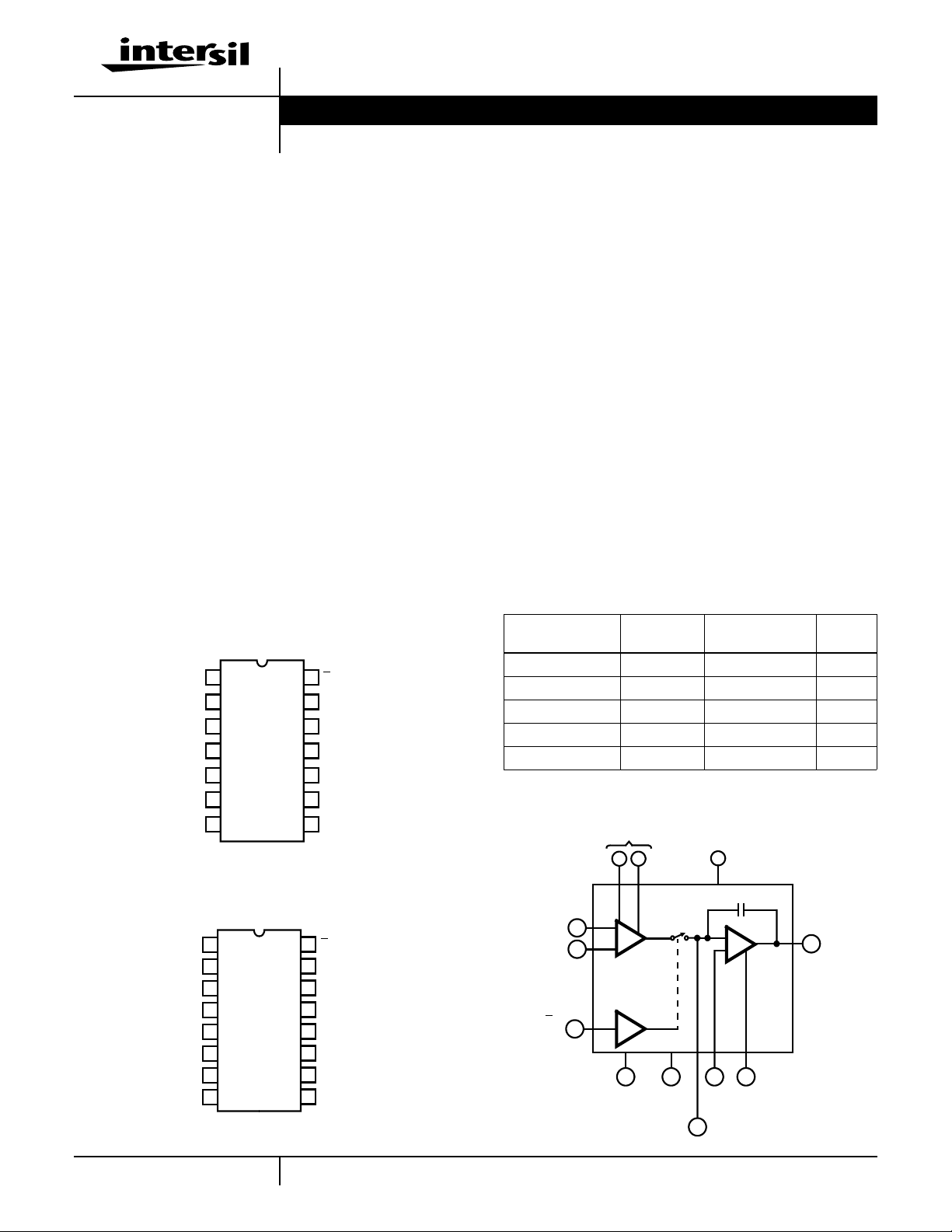
Pinouts
HA-5320
(PDIP, CERDIP)
TOP VIEW
-INPUT
+INPUT
OFFSET ADJUST
OFFSET ADJUST
SIG. GND
OUTPUT
-INPUT
+INPUT
OFFSET ADJUST
OFFSET ADJUST
SIG. GND
OUTPUT
NC
V-
V-
1
2
3
4
5
6
7
HA-5320
(SOIC)
TOP VIEW
1
2
3
4
5
6
7
8
S/H CONTROL
14
13
SUPPLY GND
12
NC
11
C
EXT
10
NC
9
V+
INTEGRATOR
8
BANDWIDTH
16
S/H CONTROL
SUPPLY GND
15
NC
14
C
13
EXT
NC
12
V+
11
INTEGRATOR
10
BANDWIDTH
NC
9
File Number 2857.4
Features
• Gain, DC. . . . . . . . . . . . . . . . . . . . . . . . . . . . . 2 x 10⁶ V/V
• Acquisition Time. . . . . . . . . . . . . . . . . . . . . 1.0µs (0.01%)
o
• Droop Rate. . . . . . . . . . . . . . . . . . . . . . 0.08µV/µs (25
C)
17µV/µs (Full Temperature)
• Aperture Time . . . . . . . . . . . . . . . . . . . . . . . . . . . . . 25ns
• Hold Step Error (See Glossary) . . . . . . . . . . . . . . . . . 5mV
• Internal Hold Capacitor
• Fully Differential Input
• TTL Compatible
Applications
• Precision Data Acquisition Systems
• Digital to Analog Converter Deglitcher
• Auto Zero Circuits
• Peak Detector
Ordering Information
TEMP.
PART NUMBER
RANGE (oC) PACKAGE
HA1-5320-2 -55 to 25 14 Ld CERDIP F14.3
HA1-5320-5 0 to 75 14 Ld CERDIP F14.3
HA3-5320-5 0 to 75 14 Ld PDIP E14.3
HA9P5320-5 0 to 75 16 Ld SOIC M16.3
HA9P5320-9 -40 to 85 16 Ld SOIC M16.3
PKG.
NO.
Functional Diagram
OFFSET
-INPUT
+INPUT
S/H
CONTROL
ADJUST
3 4
HA-5320
1
2
14
13
SUPPLY
GND
V+
9
100pF
-
+
5 6 8
V-
SIG.
GND
C
11
EXT
7
INTEGRATOR
BANDWIDTH
OUTPUT
1
CAUTION: These devices are sensitive to electrostatic discharge; follow proper IC Handling Procedures.
1-888-INTERSIL or 321-724-7143
| Copyright © Intersil Corporation 1999
Page 2
HA-5320
Absolute Maximum Ratings Thermal Information
Supply Voltage. . . . . . . . . . . . . . . . . . . . . . . . . . . . . . . . . . . . . . .40V
Differential Input Voltage . . . . . . . . . . . . . . . . . . . . . . . . . . . . . . .24V
Digital Input Voltage. . . . . . . . . . . . . . . . . . . . . . . . . . . . . +8V, -15V
Output Current, Continuous (Note 1). . . . . . . . . . . . . . . . . . . ±20mA
Operating Conditions
Temperature Range
HA-5320-2 . . . . . . . . . . . . . . . . . . . . . . . . . . . . . . -55oC to 125oC
HA-5320-5 . . . . . . . . . . . . . . . . . . . . . . . . . . . . . . . . 0oC to 75oC
HA-5320-9 . . . . . . . . . . . . . . . . . . . . . . . . . . . . . . . -40oCto85oC
Supply Voltage Range (Typical, Note 2) . . . . . . . . . ±13.5V to ±20V
CAUTION: Stresses above those listed in “Absolute Maximum Ratings” may cause permanent damage to the device. This is a stress only rating and operation of the
device at these or any other conditions above those indicated in the operational sections of this specification is not implied.
NOTES:
1. Internal Power Dissipation may limit Output Current below 20mA.
2. Specification based on a one time characterization. This parameter is not guaranteed.
3. θJA is measured with the component mounted on an evaluation PC board in free air.
Thermal Resistance (Typical, Note 3) θJA (oC/W) θJC (oC/W)
CERDIP Package. . . . . . . . . . . . . . . . . 70 18
PDIP Package . . . . . . . . . . . . . . . . . . . 75 N/A
SOIC Package . . . . . . . . . . . . . . . . . . . 90 N/A
Maximum Junction Temperature (Ceramic Package) . . . . . . . . .175oC
Maximum Junction Temperature (Plastic Package) . . . . . . . .150oC
Maximum Storage Temperature Range. . . . . . . . . . -65oC to 150oC
Maximum Lead Temperature (Soldering 10s) . . . . . . . . . . . . 300oC
(SOIC - Lead Tips Only)
Electrical Specifications V
Unity Gain Configuration (Output tied to -Input), Unless Otherwise Specified
PARAMETER
INPUT CHARACTERISTICS
Input Voltage Range Full ±10 - - ±10 - - V
Input Resistance 25 1 5 - 1 5 - MΩ
Input Capacitance 25 - - 5 - - 5 pF
Offset Voltage 25 - 0.2 - - 0.5 - mV
Bias Current 25 - 70 200 - 100 300 nA
Offset Current 25 - 30 100 - 30 300 nA
Common Mode Range Full ±10 - - ±10 - - V
CMRR V
Offset Voltage Temperature Coefficient Full - 5 15 - 5 20 µV/
TRANSFER CHARACTERISTICS
Gain DC, (Note 12) 25 10
Gain Bandwidth Product
= +1, Note 5)
(A
V
OUTPUT CHARACTERISTICS
Output Voltage Full ±10 - - ±10 - - V
Output Current 25 ±10 - - ±10 - - mA
Full Power Bandwidth Note 4 25 - 600 - - 600 - kHz
Output Resistance Hold Mode 25 - 1.0 - - 1.0 - Ω
Total Output Noise (DC to 10MHz) Sample 25 - 125 200 - 125 200 µV
= ±5.0V; CH = Internal; Digital Input: VIL = +0.8V (Sample), VIH = +2.0V (Hold),
SUPPLY
TEST
CONDITIONS
= ±5V 25 80 90 - 72 90 - dB
CM
CH = 100pF 25 - 2.0 - - 2.0 - MHz
= 1000pF 25 - 0.18 - - 0.18 - MHz
C
H
Hold 25 - 125 200 - 125 200 µV
TEMP.
o
C)
(
Full - - 2.0 - - 1.5 mV
Full - - 200 - - 300 nA
Full - - 100 - - 300 nA
HA-5320-2/-9 HA-5320-5
6
2 x 10
6
- 3 x 1052 x 10
6
- V/V
UNITSMIN TYP MAX MIN TYP MAX
o
RMS
RMS
C
2
Page 3
HA-5320
Electrical Specifications V
= ±5.0V; CH = Internal; Digital Input: VIL = +0.8V (Sample), VIH = +2.0V (Hold),
SUPPLY
Unity Gain Configuration (Output tied to -Input), Unless Otherwise Specified (Continued)
HA-5320-2/-9 HA-5320-5
UNITSMIN TYP MAX MIN TYP MAX
PARAMETER
TEST
CONDITIONS
TEMP.
o
(
C)
TRANSIENT RESPONSE
Rise Time Note 5 25 - 100 - - 100 - ns
Overshoot Note 5 25 - 15 - - 15 - %
Slew Rate Note 6 25 - 45 - - 45 - V/µs
DIGITAL INPUT CHARACTERISTICS
Input Voltage V
Input Current V
IH
V
IL
= 0V 25 - - 4 - - 4 µA
IL
Full 2.0 - - 2.0 - - V
Full - - 0.8 - - 0.8 V
Full - - 10 - - 10 µA
= +5V Full - - 0.1 - - 0.1 µA
V
IH
SAMPLE AND HOLD CHARACTERISTICS
Acquisition Time (Note 7) To 0.1% 25 - 0.8 1.2 - 0.8 1.2 µs
To 0.01% 25 - 1.0 1.5 - 1.0 1.5 µs
Aperture Time (Note 8) 25 - 25 - - 25 - ns
Effective Aperture Delay Time 25 -50 -25 0 -50 -25 0 ns
Aperture Uncertainty 25 - 0.3 - - 0.3 - ns
Droop Rate 25 - 0.08 0.5 - 0.08 0.5 µV/µs
Full - 17 100 - 1.2 100 µV/µs
Drift Current Note 9 25 - 8 50 - 8 50 pA
Full - 1.7 10 - 0.12 10 nA
Charge Transfer Note 9 25 - 0.5 1.1 - 0.5 1.1 pC
Hold Step Error Note 9 25 - 5 11 - 5 11 mV
Hold Mode Settling Time To 0.01% Full - 165 350 - 165 350 ns
Hold Mode Feedthrough 10V
, 100kHz Full - 2 - - 2 - mV
P-P
POWER SUPPLY CHARACTERISTICS
Positive Supply Current Note 10 25 - 11 13 - 11 13 mA
Negative Supply Current Note 10 25 - -11 -13 - -11 -13 mA
Supply Voltage Range Note 2 ±13.5 −±20 ±13.5 - ±20 V
Power Supply Rejection V+, Note 11 Full 80 - - 80 - - dB
V-, Note 11 Full 65 - - 65 - - dB
NOTES:
= 20V
4. V
O
5. VO = 200mV
; RL = 2kΩ; CL = 50pF; unattenuated output.
P-P
; RL = 2kΩ; CL = 50pF.
P-P
6. VO = 20V Step; RL = 2kΩ; CL = 50pF.
7. VO = 10V Step; RL = 2kΩ; CL = 50pF.
8. Derived from computer simulation only; not tested.
9. VIN = 0V, VIH = +3.5V, tR < 20ns (VIL to VIH).
10. Specified for a zero differential input voltage between +IN and -IN. Supply current will increase with differential input (as may occur in the Hold
mode) to approximately ±46mA at 20V.
11. Based on a 1V delta in each supply, i.e. 15V ±0.5VDC.
12. RL = 1kΩ, CL = 30pF.
3
Page 4

Test Circuits and Waveforms
HA-5320
S/H CONTROL
V
O
V
P
NOTES:
13. Observe the “hold step” voltage VP.
14. Compute charge transfer: Q = VPCH.
FIGURE 2. CHARGE TRANSFER TEST FIGURE 3. DRIFT CURRENT TEST
ANALOG
MUX OR
SWITCH
A
IN
10V
P-P
100kHz
SINE WAVE
S/H CONTROL
INPUT
V
IN
1
S/H
CONTROL
INPUT
-INPUT
2
+INPUT
14
S/H CONTROL
HA-5320
OUTPUT
(CH = 100pF)
FIGURE 1. CHARGE TRANSFER AND DRIFT CURRENT
HOLD (+3.5V)
SAMPLE (0V)
S/H CONTROL
V
O
NOTES:
15. Observe the voltage “droop”, ∆VO/∆t.
16. Measure the slope of the output during hold, ∆VO/∆t, and
compute drift current: ID = CH∆VO/∆t.
V-V+
HA-5320
95
1
-IN
2
+IN
S/H CONTROL
14
SUPPLY
GND
13 11 6
TO
SUPPLY
COMMON
C
NC
EXT
REF
COM
TO
SIGNAL
GND
INT.
COMP.
8
NC
OUT
7
V
7
8
11
OUT
NC
NC
NOTE:
Feedthrough in
V
V
O
dB 20
= V
OUT
∆V
∆t
V
OUT
-------------- -
log=
P-P
where:
V
IN
, Hold Mode, VIN = V
HOLD (+3.5V)
SAMPLE (0V)
O
P-P
.
FIGURE 4. HOLD MODE FEEDTHROUGH ATTENUATION
Application Information
The HA-5320 has the uncommitted differential inputs of an
op amp, allowing the Sample and Hold function to be
combined with many conventional op amp circuits. See the
Intersil Application Note AN517 for a collection of circuit
ideas.
Layout
A printed circuit board with ground plane is recommended
for best performance. Bypass capacitors (0.01µF to 0.1µF,
ceramic) should be provided from each power supply
terminal to the Supply Ground terminal on pin 13.
The ideal ground connections are pin 6 (SIG. Ground)
directly to the system Signal Ground, and pin 13 (Supply
Ground) directly to the system Supply Common.
4
Hold Capacitor
The HA-5320 includes a 100pF MOS hold capacitor,
sufficient for most high speed applications (the Electrical
Specifications section is based on this internal capacitor).
Additional capacitance may be added between pins 7 and
11. This external hold capacitance will reduce droop rate at
the expense of acquisition time, and provide other trade-offs
as shown in the Performance Curves.
If an external hold capacitor C
bandwidth capacitor of value 0.1C
from pin 8 to ground. Exact value and type are not critical.
The hold capacitor C
should have high insulation
EXT
resistance and low dielectric absorption, to minimize droop
errors. Polystyrene dielectric is a good choice for operating
temperatures up to 85
good performance to 125
o
C. Teflon®and glass dielectrics offer
o
C and above.
®Teflon is a registered Trademark of Dupont Corporation.
is used, then a noise
EXT
should be connected
EXT
Page 5

HA-5320
The hold capacitor terminal (pin 11) remains at virtual
ground potential. Any PC connection to this terminal should
be kept short and “guarded” by the ground plane, since
nearby signal lines or power supply voltages will introduce
errors due to drift current.
Typical Application
Figure 5 shows the HA-5320 connected as a unity gain
noninverting amplifier - its most widely used configuration.
As an input device for a fast successive - approximation A/D
converter, it offers very high throughput rate for a monolithic
IC sample/hold amplifier. Also, the HA-5320’shold step error
is adjustable to zero using the Offset Adjust potentiometer,
to deliver a 12-bit accurate output from the converter.
The application may call foran external hold capacitor C
shown.As mentioned earlier,0.1C
is then recommended at
EXT
EXT
as
pin 8 to reduce output noise in the Hold mode.
The HA-5320 output circuit does not include short circuit
protection, and consequently its output impedance remains
low at high frequencies. Thus, the step changes in load
current which occur during an A/D conversion are absorbed
at the S/H output with minimum voltage error. A momentary
short circuit to ground is permissible, but the output is not
designed to tolerate a short of indefinite duration.
Glossary of Terms
Acquisition Time
The time required following a “sample” command, f or the
output to reach its final value within ±0.1% or ±0.01%. This is
the minimum sample time required to obtain a givenaccuracy,
and includes switch delay time , slewing time and settling time.
Charge Transfer
The small charge transferred to the holding capacitor from
the inter-electrode capacitance of the switch when the unit is
switched to the HOLD mode. Charge transfer is directly
proportional to sample-to-hold offset pedestal error, where:
Charge Transfer (pC) = C
(pF) x Hold Step Error (V)
H
10kΩ
OFFSET
ADJUST
±15mV
3459
-15V +15V
11
C
EXT
Aperture Time
The time required for the sample-and-hold switch to open,
independent of delays through the switch driver and input
amplifier circuitry. The switch opening time is the interval
between the conditions of 10% open and 90% open.
Hold Step Error
Hold Step Error is the output error due to Charge Transfer(see
above). It may be calculated from the specified par ameter,
Charge Transfer , using the following relationship:
Hold Step (V)
Charge Transfer (pC)
----------------------------------------------------------- -=
Hold Capacitance (pF)
See Performance Curves.
Effective Aperture Delay Time (EADT)
The difference between the digital delay time from the Hold
command to the opening of the S/H switch, and the
propagation time from the analog input to the switch.
EADT may be positive, negative or zero. If zero , the S/H
amplifier will output a voltage equal to V
at the instant the
IN
Hold command was received. For negative EADT,the output in
Hold (exclusive of pedestal and droop errors) will correspond to
a value of V
that occurred before the Hold command.
IN
Aperture Uncertainty
The range of variation in Effectiv e Aperture Delay Time.
Aperture Uncertainty (also called Aperture Delay Uncertainty ,
Aperture Time Jitter, etc.) sets a limit on the accuracy with
which a waveform can be reconstructed from sample data.
Drift Current
The net leakage current from the hold capacitor during the
hold mode. Drift current can be calculated from the droop
rate using the formula:
∆V
I
(pA) CHpF()
D
------- -
(V/s)×=
∆t
HI-574A
V
S/H CONTROL
H
S
1
IN
2
14
+
-
HA-5320
13
SYSTEM POWER
GROUND
FIGURE 5. TYPICAL HA-5320 CONNECTIONS; NONINVERTING UNITY GAIN MODE
68
100pF
-
+
0.1C
EXT
SYSTEM SIGNAL
GROUND
7
CONVERT
13
5
9
INPUT
R/
C
ANALOG
COMMON
DIGITAL
OUTPUT
NOTE: Pin Numbers Refer to
DIP PackageOnly.
5
Page 6

Typical Performance Curves
HA-5320
10
5
1.0
0.5
0.1
SAMPLE-TO-HOLD OFFSET
0.05
0.01
(HOLD STEP) ERROR, (mV)
100 1000 10K 100K
C
VALUE (pF)
H
ACQUISITION TIME FOR
10V STEP TO +0.01% (µs)
VOLTAGE DROOP DURING
HOLD MODE, (mV/100ms)
FIGURE 6. TYPICAL SAMPLE AND HOLD PERFORMANCE
AS A FUNCTION OF HOLD CAPACITOR
120
100
80
60
GAIN (dB)
40
20
GAIN
(C
= 1100pF)
H
CH = 100pF, INTERNAL
1000
100
(pA)
DRIFT
10
I
1
0
-25 0 25 50 75 100 125
TEMPERATURE (
FIGURE 7. DRIFT CURRENT vs TEMPERATURE
0
45
PHASE
(CH = 100pF)
GAIN
90
135
PHASE (DEGREES)
180
o
C)
0
0
10 100 1K 10K 100K 1M 10M
FREQUENCY (Hz)
FIGURE 8. OPEN LOOP GAIN AND PHASE RESPONSE
CH = 100pF
HOLD STEP VOLTAGE (mV)
= 25oC
T
A
5.0
0.5
0.05
-10 -8 -6 -4 -2 2 4 6 8 10
DC INPUT (V)
CH = 100pF
C
= 1000pF
H
= 0.01µF
C
H
HOLD STEP VOLTAGE
2345
LOGIC LEVEL HIGH (V)
75oC
25oC
FIGURE 9A. HOLD STEP vs INPUT VOLTAGE FIGURE 9B. HOLD STEP vs LOGIC (VIH) VOLTAGE
FIGURE 9. TYPICAL SAMPLE-TO-HOLD OFFSET (HOLD STEP) ERROR
6
Page 7

Die Characteristics
HA-5320
DIE DIMENSIONS:
92 mils x 152 mils x 19 mils
METALLIZATION:
Type: Al, 1% Cu
Thickness: 16k
Å ±2kÅ
Metallization Mask Layout
SUPPLY GND
S/H CTRL (14)
-INPUT (1)
HA-5320
PASSIVATION:
Type: Nitride (Si
Silox Thickness: 12k
) over Silox (SiO2, 5% Phos)
3N4
Å ±2kÅ
Nitride Thickness: 3.5kÅ ±1.5kÅ
TRANSISTOR COUNT:
184
SUBSTRATE POTENTIAL:
V-
C
EXT
V+
(9)(11)(13)
(8) INT BW
(7) OUTPUT
+INPUT (2)
(3)
(4)
VIO ADJVIO ADJ
(5)
V-
(6) SIG GND
All Intersil semiconductor products are manufactured, assembled and tested under ISO9000 quality systems certification.
Intersil semiconductor products are sold by description only. Intersil Corporation reserves the right to make changes in circuit design and/or specifications at any time without notice. Accordingly ,the reader is cautioned to verify that data sheets are current before placing orders. Information furnished by Intersil is believed to be accurate and
reliable. However, no responsibility is assumed by Intersil or its subsidiaries for its use; nor for any infringements of patents or other rights of third parties which may result
from its use. No license is granted by implication or otherwise under any patent or patent rights of Intersil or its subsidiaries.
For information regarding Intersil Corporation and its products, see web site www.intersil.com
Sales Office Headquarters
NORTH AMERICA
Intersil Corporation
P. O. Box 883, Mail Stop 53-204
Melbourne, FL 32902
TEL: (321) 724-7000
FAX: (321) 724-7240
EUROPE
Intersil SA
Mercure Center
100, Rue de la Fusee
1130 Brussels, Belgium
TEL: (32) 2.724.2111
FAX: (32) 2.724.22.05
ASIA
Intersil (Taiwan) Ltd.
7F-6, No. 101 Fu Hsing North Road
Taipei, Taiwan
Republic of China
TEL: (886) 2 2716 9310
FAX: (886) 2 2715 3029
7
 Loading...