

Page 1
TM
HA-5221
Data Sheet April 2000
100MHz, Low Noise, Precision
Operational Amplifier
The HA-5221 is a single high performance dielectrically
isolated, op amp, featuring precision DC characteristics while
providing excellent A C char acteristics. Designed for audio,
video,and other demanding applications, noise (3.4nV/√
1kHz), total harmonic distortion (<0.005%), and DC errors are
kept to a minimum.
The precision performance is shown by low offset voltage
(0.3mV), low bias currents (40nA), low offset currents
(15nA), and high open loop gain (128dB). The combination
of these excellent DC characteristics with the fast settling
time (0.4µs) makes the HA-5221 ideally suited for precision
signal conditioning.
The unique design of the HA-5221 gives it outstanding AC
characteristics not normally associated with precision op
amps, high unity gain bandwidth (35MHz) and high slew rate
(25V/µs). Other key specifications include high CMRR (95dB)
and high PSRR (100dB). The combination of these
specifications will allow the HA-5221 to be used in RF signal
conditioning as well as video amplifiers.
For MIL-STD-883C compliant product and Ceramic LCC
packaging, consult the HA-5221/883C data sheet. (Intersil
AnswerFAX (321-724-7800) Document #3716.)
Hz at
File Number 2915.5
Features
• Gain Bandwidth Product. . . . . . . . . . . . . . . . . . . . 100MHz
• Unity Gain Bandwidth. . . . . . . . . . . . . . . . . . . . . . . 35MHz
• Slew Rate. . . . . . . . . . . . . . . . . . . . . . . . . . . . . . . . 25V/µs
• Low Offset Voltage . . . . . . . . . . . . . . . . . . . . . . . . . 0.3mV
• High Open Loop Gain. . . . . . . . . . . . . . . . . . . . . . . 128dB
• Low Noise Voltage at 1kHz. . . . . . . . . . . . . . . . 3.4nV/√
Hz
• High Output Current. . . . . . . . . . . . . . . . . . . . . . . . . 56mA
• Low Supply Current . . . . . . . . . . . . . . . . . . . . . . . . . . 8mA
Applications
• Precision Test Systems
• Active Filtering
• Small Signal Video
• Accurate Signal Processing
• RF Signal Conditioning
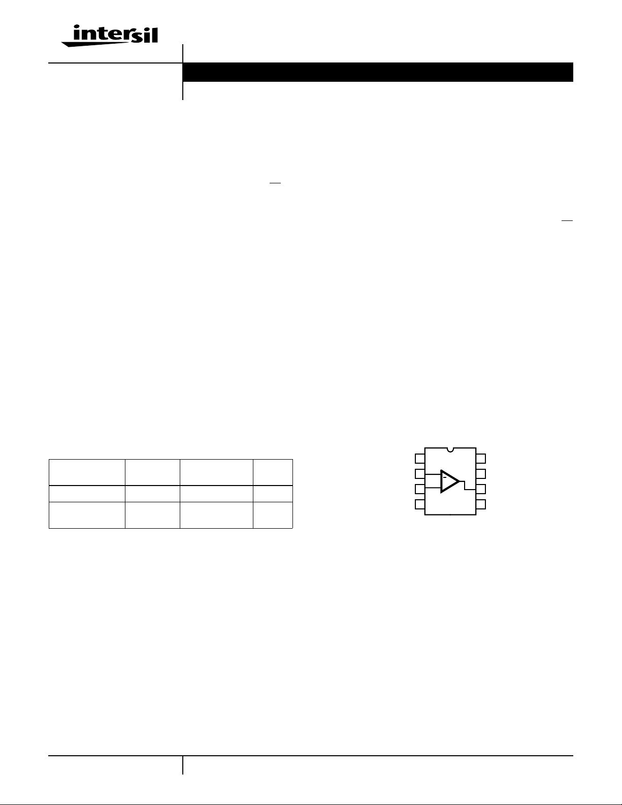
Pinout
HA-5221
(CERDIP, SOIC)
TOP VIEW
Ordering Information
PART NUMBER
(BRAND)
HA7-5221-5 0 to 75 8 Ld CERDIP F8.3A
HA9P5221-5
(H52215)
TEMP.
RANGE (oC) PACKAGE
0 to 75 8 Ld SOIC M8.15
PKG.
NO.
-BAL
-IN
+IN
V-
1
2
+
3
4
8
7
6
5
+BAL
V+
OUT
NC
1
1-888-INTERSIL or 321-724-7143 | Intersil and Design is a trademark of Intersil Corporation. | Copyright © Intersil Corporation 2000
CAUTION: These devices are sensitive to electrostatic discharge; follow proper IC Handling Procedures.
Page 2
HA-5221
Absolute Maximum Ratings Thermal Information
Supply Voltage Between V+ and V- Terminals. . . . . . . . . . . . . . 35V
Differential Input Voltage (Note 1) . . . . . . . . . . . . . . . . . . . . . . . . 5V
Output Current Short Circuit Duration . . . . . . . . . . . . . . . . Indefinite
Operating Conditions
Temperature Range
HA-5221-5 . . . . . . . . . . . . . . . . . . . . . . . . . . . . . . . . 0oC to 75oC
CAUTION: Stresses above those listed in “Absolute Maximum Ratings” may cause permanent damage to the device. This is a stress only rating and operation of the
device at these or any other conditions above those indicated in the operational sections of this specification is not implied.
NOTES:
1. Input is protected by back-to-back zener diodes. See applications section.
2. θJA is measured with the component mounted on an evaluation PC board in free air.
Thermal Resistance (Typical, Note 2) θJA (oC/W) θJC (oC/W)
CERDIP Package. . . . . . . . . . . . . . . . . 135 50
SOIC Package . . . . . . . . . . . . . . . . . . . 157 N/A
Maximum Junction Temperature (Hermetic Package) . . . . . . . 175oC
Maximum Junction Temperature (Plastic Package) . . . . . . . 150oC
Maximum Storage Temperature Range. . . . . . . . . . -65oC to 150oC
Maximum Lead Temperature (Soldering 10s) . . . . . . . . . . . . 300oC
(SOIC - Lead Tips Only)
Electrical Specifications V
PARAMETER TEST CONDITIONS TEMP. (oC) MIN TYP MAX UNITS
INPUT CHARACTERISTICS
Input Offset Voltage 25 - 0.30 0.75 mV
Average Offset Voltage Drift Full - 0.5 - µV/oC
Input Bias Current 25 - 40 100 nA
Input Offset Current 25 - 15 100 nA
Input Offset Voltage Match 25 - 400 750 µV
Common Mode Range 25 ±12 - - V
Differential Input Resistance 25 - 70 - kΩ
Input Noise Voltage f = 0.1Hz to 10Hz 25 - 0.25 - µV
Input Noise Voltage Density (Notes 3, 11) f = 10Hz 25 - 6.2 10 nV/√Hz
= ±15V, Unless Otherwise Specified
SUPPLY
Full - 0.35 1.5 mV
Full - 70 200 nA
Full - 30 150 nA
Full - - 1500 µV
f = 100Hz 25 - 3.6 6 nV/√Hz
P-P
f = 1000Hz 25 - 3.4 4.0 nV/√Hz
Input Noise Current Density (Notes 3, 11) f = 10Hz 25 - 4.7 8.0 pA/√Hz
f = 100Hz 25 - 1.8 2.8 pA/√Hz
f = 1000Hz 25 - 0.97 1.8 pA/√Hz
THD+N Note 4 25 - <0.005 - %
TRANSFER CHARACTERISTICS
Large Signal Voltage Gain Note 5 25 106 128 - dB
Full 100 120 - dB
CMRR VCM = ±10V Full 86 95 - dB
Unity Gain Bandwidth -3dB 25 - 35 - MHz
2
Page 3
HA-5221
Electrical Specifications V
= ±15V, Unless Otherwise Specified (Continued)
SUPPLY
PARAMETER TEST CONDITIONS TEMP. (oC) MIN TYP MAX UNITS
Gain Bandwidth Product 1kHz to 400kHz 25 - 100 - MHz
Minimum Stable Gain Full 1 - - V/V
OUTPUT CHARACTERISTICS
Output Voltage Swing RL = 333Ω Full ±10 - - V
RL = 1kΩ 25 ±12 ±12.5 - V
RL = 1kΩ Full ±11.5 ±12.1 - V
Output Current V
= ±10V Full ±30 ±56 - mA
OUT
Output Resistance 25 - 10 - Ω
Full Power Bandwidth Note 6 25 239 398 - kHz
TRANSIENT RESPONSE (Note 11)
Slew Rate Notes 7, 11 Full 15 25 - V/µs
Rise Time Notes 8, 11 Full - 13 20 ns
Overshoot Notes 8, 11 Full - 28 50 %
Settling Time (Notes 9, 10) 0.1% 25 - 0.4 - µs
0.01% 25 - 1.5 - µs
POWER SUPPLY
PSRR VS = ±10V to ±20V Full 86 100 - dB
Supply Current Full - 8 11 mA
NOTES:
3. Refer to typical performance curve in data sheet.
4. A
= 10, fO = 1kHz, VO = 5V
VCL
5. V
= 0 to ±10V, RL = 1kΩ, CL = 50pF.
OUT
6. Full Power Bandwidth is calculated by: FPBW = .
7. V
8. V
= ±2.5V, RL = 1kΩ, CL = 50pF.
OUT
= ±100mV, RL = 1kΩ, CL = 50pF.
OUT
, RL = 600Ω, 10Hz to 100kHz, minimum resolution of test equipment is 0.005%.
RMS
Slew Rate
-------------------------- -
2πV
PEAK
V
PEAK
10V=,
9. Settling time is specified for a 10V step and AV = -1.
10. See Test Circuits.
11. Guaranteed by characterization.
Test Circuits and Waveforms
V
IN
+
-
1kΩ
50pF
V
OUT
FIGURE 1. TRANSIENT RESPONSE TEST CIRCUIT
3
Page 4
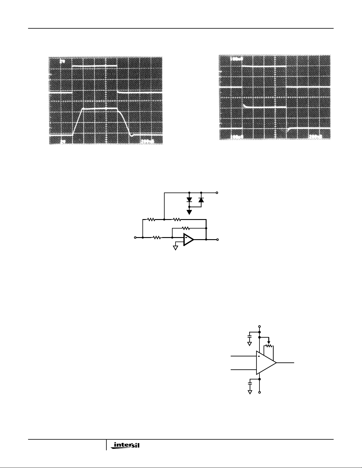
Test Circuits and Waveforms (Continued)
HA-5221
2.5V
0V
-2.5V
2.5V
0V
-2.5V
100mV
0V
V
IN
-100mV
100mV
0V
V
OUT
-100mV
V
= ±100mV
V
= 2.5V
OUT
Vertical Scale = 2V/Div.,
Horizontal Scale = 200ns/Div.
OUT
Vertical Scale = 100mV/Div.,
Horizontal Scale = 200ns/Div.
FIGURE 2. LARGE SIGNAL RESPONSE FIGURE 3. SMALL SIGNAL RESPONSE
V
SETTLE
5K
V
IN
2K
5K
2K
V
+
OUT
NOTES:
12. AV= -1.
13. Feedback and summing resistors must be matched (0.1%).
14. HP5082-2810 clipping diodes recommended.
15. Tektronix P6201 FET probe used at settling point.
FIGURE 4. SETTLING TIME TEST CIRCUIT
Application Information
Operation at Various Supply Voltages
The HA-5221 operates over a wide range of supply voltages
with little variation in performance. The supplies may be
varied from ±5V to ±15V.See typical performance curves for
variations in supply current, slew rate and output voltage
swing.
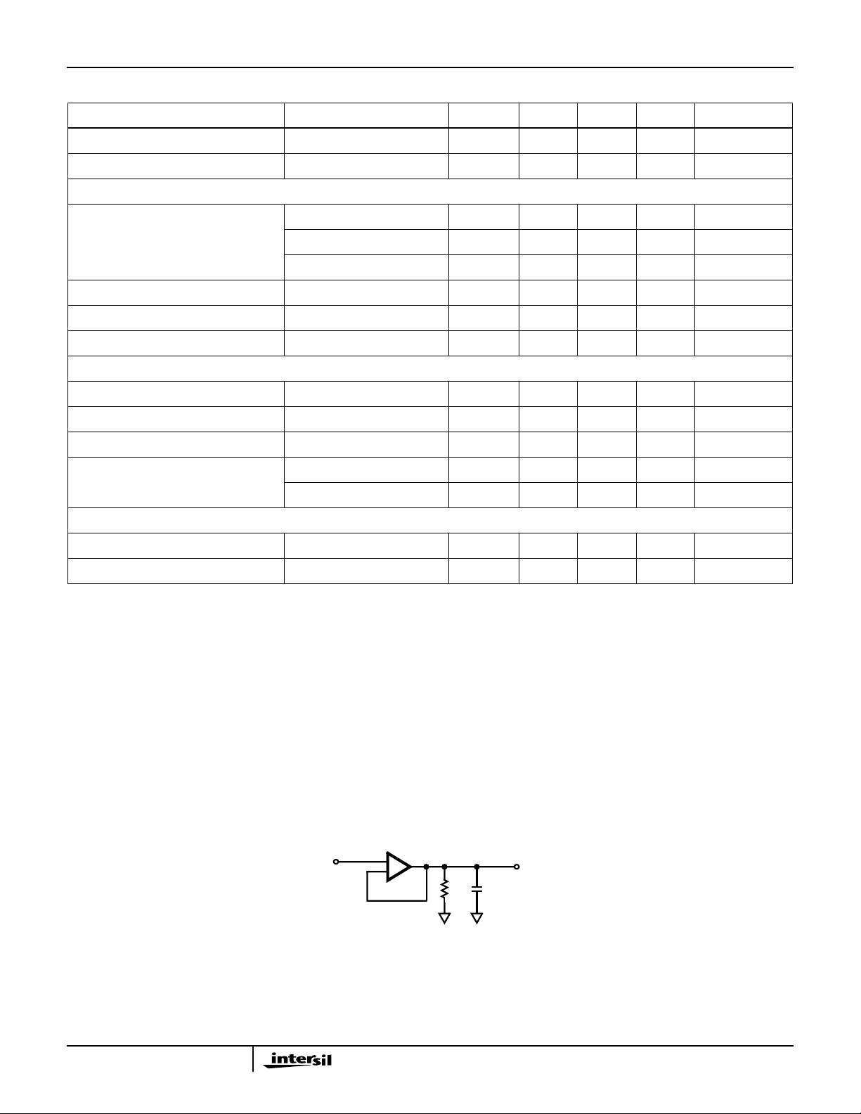
Offset Adjustment
The following diagram shows the offset voltage adjustment
configuration for the HA-5221. By moving the potentiometer
wiper towards pin 8 (+BAL), the op amps output voltage will
increase; towards pin 1 (-BAL) decreases the output voltage.
A 20kΩ trim pot will allow an offset voltage adjustment of
about 10mV.
+15V
7
R
2
3
P
1
8
6
+
4
-15V
Capacitive Loading Considerations
When driving capacitive loads >80pF, a small resistor, 50Ω
to 100Ω, should be connected in series with the output and
inside the feedback loop.
4
Page 5

HA-5221
Saturation Recovery
When an op amp is over driven, output devices can saturate
and sometimes take a long time to recover. By clamping the
input, output saturation can be avoided. If output saturation
can not be avoided, the maximum recovery time when
overdriven into the positive rail is 10.6µs. When driven into
the negative rail the maximum recovery time is 3.8µs.
Input Protection
The HA-5221 has built in back-to-back protection diodes
which limit the maximum allowable differential input voltage
to approximately 5V. If the HA-5221 is used in circuits where
the maximum differential voltage may be exceeded, then
current limiting resistors must be used. The input current
should be limited to a maximum of 10mA.
Typical Performance Curves V
RL = 1K, CL = 50pF
120
100
80
60
40
GAIN (dB)
20
0
1K 10K 100K 1M 100M
GAIN
PHASE
FREQUENCY (Hz)
= ±15V, TA = 25oC
S
180
135
90
45
0
10M
∆V
PC Board Layout Guidelines
When designing with the HA-5221, good high frequency
(RF) techniques should be used when building a PC board.
Use of ground plane is recommended. Power supply
decoupling is very important. A 0.01µF to 0.1µF high quality
ceramic capacitor at each power supply pin with a 2.2µF to
10µF tantalum close by will provide excellent decoupling.
Chip capacitors produce the best results due to ease of
placement next to the op amp and basically no lead
inductance. If leaded capacitors are used, the leads should
be kept as short as possible to minimize lead inductance.
12
9
A
= +1, RL = 1K, CL = 50pF
V
6
3
0
GAIN (dB)
-3
-6
PHASE MARGIN (DEGREES)
10K 100K 1M 100M
R
LIMIT
2
IN
R
LIMIT
3
GAIN
PHASE
FREQUENCY (Hz)
6
10M
V
OUT
180
135
90
45
PHASE MARGIN (DEGREES)
0
+
FIGURE 5. OPEN LOOP GAIN AND PHASE vs FREQUENCY FIGURE 6. CLOSED LOOP GAIN vs FREQUENCY
9
AV = -1, RL = 1K, CL = 50pF
6
3
GAIN (dB)
0
10K 100K 1M 100M
GAIN
PHASE
10M
FREQUENCY (Hz)
180
135
90
45
0
PHASE MARGIN (DEGREES)
80
AV = -1000
60
AV = -100
40
AV = -10
20
0
CLOSED LOOP GAIN (dB)
10K 100K 1M 100M
AV = -10
AV = -1000
FREQUENCY (Hz)
RL = 1K, CL = 50pF
AV = -100
10M
FIGURE 7. CLOSED LOOP GAIN vs FREQUENCY FIGURE 8. VARIOUS CLOSED LOOP GAINS vs FREQUENCY
5
180
135
90
45
0
PHASE MARGIN (DEGREES)
Page 6

HA-5221
Typical Performance Curves V
AV = +1, RL = 1K
120
100
80
60
40
CMRR (dB)
20
0
10K 100K 1M 100M10M
FREQUENCY (Hz)
S
FIGURE 9. CMRR vs FREQUENCY FIGURE 10. PSRR vs FREQUENCY
20
R
= 1K
L
18
16
14
12
10
8
6
OPEN LOOP GAIN (V/µV)
4
2
0
-60 -40 -20 0 20 40 60 80 100 120
TEMPERATURE (oC)
= ±15V, TA = 25oC (Continued)
100
PSRR (dB)
OFFSET VOLTAGE (µV)
AV = +1, RL = 1K
80
60
40
20
0
10K 100K 1M 100M10M
300
250
200
150
100
50
0
-50
-100
-60 -40 -20 0 20 40 60 80 100 120
-PSRR
+PSRR
FREQUENCY (Hz)
TEMPERATURE (oC)
FIGURE 11. OPEN LOOP GAIN vs TEMPERATURE FIGURE 12. OFFSET VOLTAGE vs TEMPERATURE
(4 REPRESENTATIVE UNITS)
14
RL = 600Ω
13.5
160
140
120
100
80
60
40
BIAS CURRENT (nA)
20
0
-20
-40
-60 -40 -20 0 20 40 60 80 100 120
TEMPERATURE (oC)
FIGURE 13. BIAS CURRENT vs TEMPERATURE
13
12.5
12
11.5
11
PEAK OUTPUT VOLTAGE (V)
10.5
10
-60 -40 -20 0 20 40 60 80 100 120
TEMPERATURE (oC)
FIGURE 14. OUTPUT VOLTAGE SWING vs TEMPERATURE
(4 REPRESENTATIVE UNITS)
6
Page 7

HA-5221
Typical Performance Curves V
1.1
C)
o
1.05
0.95
0.85
SLEW RATE (NORMALIZED TO 1 AT 25
8.25
7.75
SUPPLY CURRENT (mA)
= +1, RL = 1K, CL = 50pF
A
V
1.0
0.9
0.8
-60 -40 -20 0 20 40 60 80 100
TEMPERATURE (oC)
FIGURE 15. SLEW RATE vs TEMPERATURE FIGURE 16. OFFSET VOLTAGE WARM-UP DRIFT
8.5
8
7.5
57911131517
SUPPLY VOLTAGE (±V)
= ±15V, TA = 25oC (Continued)
S
120
70
60
50
40
30
20
10
OFFSET VOLTAGE CHANGE (µV)
0
012345
TIME AFTER POWER UP (MINUTES)
(CERDIP PACKAGES)
36
AV = +1, RL = 2K, CL = 50pF
34
32
30
28
26
24
22
20
18
SLEW RATE (V/µs)
16
14
12
10
57911131517
+SLEW RATE
-SLEW RATE
SUPPLY VOLTAGE (±V)
FIGURE 17. SUPPLY CURRENT vs SUPPLY VOLTAGE FIGURE 18. SLEW RATE vs SUPPLY VOLTAGE
20
RL = 600Ω
16
15
10
5
PEAK OUTPUT VOLTAGE SWING (V)
0
57911131517
SUPPLY VOLTAGE (±V)
14
12
10
8
6
4
VOLTAGE NOISE (nV/√Hz)
2
0
1 10 100 1K 10K
FREQUENCY (Hz)
VOLTAGE NOISE
CURRENT NOISE
FIGURE 19. OUTPUT VOLTAGE SWING vs SUPPLY VOLTAGE FIGURE 20. NOISE CHARACTERISTICS
7
24
21
18
15
12
9
6
3
CURRENT NOISE (pA/√Hz)
0
Page 8

HA-5221
Typical Performance Curves V
100
90
80
70
60
50
40
30
20
10
0
-10
-20
-30
-40
-50
OFFSET CURRENT (nA)
-60
-70
-80
-90
-100
-60 -40 -20 0 20 40 60 80 100 120
TEMPERATURE (oC)
= ±15V, TA = 25oC (Continued)
S
FIGURE 21. OFFSET CURRENT vs TEMPERATURE
(4 REPRESENTATIVE UNITS)
45
40
35
30
PHASE MARGIN
AV = +1, RL = 1K
BANDWIDTH
120
100
80
60
115
114
113
112
111
110
109
108
107
106
105
104
103
102
101
CMRR AND PSRR (dB)
100
99
98
97
96
95
-60 -40 -20 0 20 40 60 80 100 120
TEMPERATURE (oC)
+PSRR
-PSRR
CMRR
FIGURE 22. CMRR AND PSRR vs TEMPERATURE
130
110
90
25
BANDWIDTH (MHz)
20
15
1 10 100 1000
LOAD CAPACITANCE (pF)
40
20
0
FIGURE 23. BANDWIDTH AND PHASE MARGIN vs LOAD
CAPACITANCE
Vertical Scale = 1mV/Div.; Horizontal Scale = 1s/Div.
AV = +25,000; EN = 0.168µV
P-P
RTI
70
PHASE MARGIN (DEGREE)
OUTPUT CURRENT (mA)
50
012345
FIGURE 24. SHORT CIRCUIT OUTPUT CURRENT vs TIME
Vertical Scale = 10mV/Div.; Horizontal Scale = 1s/Div.
TIME AFTER SHORT CIRCUIT (MINUTES)
AV = +25,000; EN = 1.5µV
P-P
RTI
FIGURE 25. 0.1Hz TO 10Hz NOISE FIGURE 26. 0.1Hz TO 1MHz
8
Page 9

HA-5221
Typical Performance Curves V
18
16
VS = ±18
14
VS = ±15
12
10
8
VS = ±10
6
4
PEAK OUTPUT VOLTAGE (V)
2
VS = ±5
0
10K 100K 1M 10M
AV = +1, RL = 1K, CL = 15pF, THD ≤ 0.01%
FREQUENCY (Hz)
= ±15V, TA = 25oC (Continued)
S
18
AV = +1, THD ≤ 0.01%, f = 1kHz
16
14
12
10
8
6
4
PEAK OUTPUT VOLTAGE (V)
2
0
10 100 1K 10K
LOAD RESISTANCE (Ω)
VS = ±18
VS = ±15
VS = ±10
VS = ±5
FIGURE 27. OUTPUT VOLTAGE SWING vs FREQUENCY FIGURE 28. OUTPUT VOLTAGE SWING vs LOAD RESISTANCE
10
9.5
9
8.5
8
7.5
7
SUPPLY CURRENT (mA)
6.5
6
-60 -40 -20 0 20 40 60 80 100 120
TEMPERATURE (oC)
FIGURE 29. SUPPLY CURRENT vs TEMPERATURE
9
Page 10

Die Characteristics
HA-5221
DIE DIMENSIONS:
72 mils x 94 mils
1840µm x 2400µm
METALLIZATION:
Type: Al, 1% Cu
Thickness: 16k
PASSIVATION:
Type: Nitride (Si
Silox Thickness: 12k
Nitride Thickness: 3.5kÅ ±1.5kÅ
Å ±2kÅ
) over Silox (SiO2, 5% Phos.)
3N4
Å ±2kÅ
Metallization Mask Layout
V- +IN -IN
SUBSTRATE POTENTIAL (POWERED UP):
V-
TRANSISTOR COUNT:
62
PROCESS:
Bipolar Dielectric Isolation
HA-5221
-BAL
+BAL
V+OUT
10
Page 11

HA-5221
Ceramic Dual-In-Line Frit Seal Packages (CERDIP)
c1
LEAD FINISH
-A-
-B-
bbb C A - B
S
BASE
PLANE
SEATING
PLANE
S1
b2
ccc C A - BMD
D
A
A
b
e
S
S
NOTES:
1. Index area: Anotchor a pin oneidentificationmarkshall be located adjacent to pin one and shall be located within the shaded
area shown. The manufacturer’s identification shall not be used
as a pin one identification mark.
2. The maximum limits of lead dimensions b and c or M shall be
measured at the centroid of the finished lead surfaces, when
solder dip or tin plate lead finish is applied.
3. Dimensions b1 and c1 apply to lead base metal only. Dimension
M applies to lead plating and finish thickness.
4. Corner leads (1, N, N/2, and N/2+1) may be configured with a
partial lead paddle. For this configuration dimension b3 replaces
dimension b2.
5. This dimension allows for off-center lid, meniscus, and glass
overrun.
6. Dimension Q shall be measured from the seating plane to the
base plane.
7. Measure dimension S1 at all four corners.
8. N is the maximum number of terminal positions.
9. Dimensioning and tolerancing per ANSI Y14.5M - 1982.
10. Controlling dimension: INCH
-DBASE
E
D
S
S
Q
A
-CL
METAL
b1
M
(b)
SECTION A-A
α
(c)
M
eA
eA/2
aaa C A - B
M
c
D
S
S
F8.3A MIL-STD-1835 GDIP1-T8 (D-4, CONFIGURATION A)
8 LEAD CERAMIC DUAL-IN-LINE FRIT SEAL PACKAGE
INCHES MILLIMETERS
SYMBOL
A - 0.200 - 5.08 -
b 0.014 0.026 0.36 0.66 2
b1 0.014 0.023 0.36 0.58 3
b2 0.045 0.065 1.14 1.65 b3 0.023 0.045 0.58 1.14 4
c 0.008 0.018 0.20 0.46 2
c1 0.008 0.015 0.20 0.38 3
D - 0.405 - 10.29 5
E 0.220 0.310 5.59 7.87 5
e 0.100 BSC 2.54 BSC -
eA 0.300 BSC 7.62 BSC -
eA/2 0.150 BSC 3.81 BSC -
L 0.125 0.200 3.18 5.08 -
Q 0.015 0.060 0.38 1.52 6
S1 0.005 - 0.13 - 7
o
α
90
105
o
90
o
105
aaa - 0.015 - 0.38 bbb - 0.030 - 0.76 -
ccc - 0.010 - 0.25 -
M - 0.0015 - 0.038 2, 3
N8 88
NOTESMIN MAX MIN MAX
o
Rev. 0 4/94
-
11
Page 12

Small Outline Plastic Packages (SOIC)
HA-5221
N
INDEX
AREA
123
-A-
E
-B-
SEATING PLANE
D
A
-C-
0.25(0.010) BM M
H
L
h x 45
o
α
e
B
0.25(0.010) C AM BS
M
NOTES:
1. Symbols are defined in the “MO Series Symbol List” in Section 2.2 of
Publication Number 95.
2. Dimensioning and tolerancing per ANSI Y14.5M-1982.
3. Dimension “D” does not include mold flash, protrusions or gate burrs.
Mold flash,protrusionandgateburrs shall not exceed 0.15mm (0.006
inch) per side.
4. Dimension “E” does not include interlead flash or protrusions. Interlead flash and protrusions shall not exceed 0.25mm (0.010 inch) per
side.
5. The chamfer on the body is optional. If it is not present, a visual index
feature must be located within the crosshatched area.
6. “L” is the length of terminal for soldering to a substrate.
7. “N” is the number of terminal positions.
8. Terminal numbers are shown for reference only.
9. The lead width “B”, as measured 0.36mm (0.014 inch) or greater
above the seating plane, shall not exceed a maximum value of
0.61mm (0.024 inch).
10. Controlling dimension: MILLIMETER. Converted inch dimensions
are not necessarily exact.
A1
C
0.10(0.004)
M8.15 (JEDEC MS-012-AA ISSUE C)
8 LEAD NARROW BODY SMALL OUTLINE PLASTIC
PACKAGE
INCHES MILLIMETERS
SYMBOL
A 0.0532 0.0688 1.35 1.75 -
A1 0.0040 0.0098 0.10 0.25 -
B 0.013 0.020 0.33 0.51 9
C 0.0075 0.0098 0.19 0.25 D 0.1890 0.1968 4.80 5.00 3
E 0.1497 0.1574 3.80 4.00 4
e 0.050 BSC 1.27 BSC H 0.2284 0.2440 5.80 6.20 h 0.0099 0.0196 0.25 0.50 5
L 0.016 0.050 0.40 1.27 6
N8 87
o
α
0
o
8
o
0
o
8
Rev. 0 12/93
NOTESMIN MAX MIN MAX
-
All Intersil semiconductor products are manufactured, assembled and tested under ISO9000 quality systems certification.
Intersil semiconductor products are sold by description only. Intersil Corporation reserves the right to make changes in circuit design and/or specifications at any time without notice. Accordingly, the reader is cautioned to verify that data sheets are current before placing orders. Information furnished by Intersil is believed to be accurate and
reliable. However, no responsibility is assumed by Intersil or its subsidiaries for its use; nor for any infringements of patents or other rights of third parties which may result
from its use. No license is granted by implication or otherwise under any patent or patent rights of Intersil or its subsidiaries.
For information regarding Intersil Corporation and its products, see web site www.intersil.com
Sales Office Headquarters
NORTH AMERICA
Intersil Corporation
P. O. Box 883, Mail Stop 53-204
Melbourne, FL 32902
TEL: (321) 724-7000
FAX: (321) 724-7240
12
EUROPE
Intersil SA
Mercure Center
100, Rue de la Fusee
1130 Brussels, Belgium
TEL: (32) 2.724.2111
FAX: (32) 2.724.22.05
ASIA
Intersil (Taiwan) Ltd.
7F-6, No. 101 Fu Hsing North Road
Taipei, Taiwan
Republic of China
TEL: (886) 2 2716 9310
FAX: (886) 2 2715 3029
 Loading...