

Page 1
June 1998
HA-5147/883
100MHz, Ultra Low Noise, Precision,
High Slew Rate Operational Amplifier
Features
• This Circuit is Processed in Accordance to MIL-STD883 and is Fully Conformant Under the Provisions of
Paragraph 1.2.1.
• High Slew Rate. . . . . . . . . . . . . . . . . . . . . . 28V/µs (Min)
• Wide Gain Bandwidth (A
• Low Noise (at 1kHz). . . . . . . . . . . . . . . 4.5nV/√
≥ 10) . . . . . . . 100MHz (Min)
V
Hz (Max)
• Low Offset Voltage. . . . . . . . . . . . . . . . . . . .100µV (Max)
o
• Low Offset Drift With Temperature. . . . 1.8µV/
C (Max)
• High CMRR. . . . . . . . . . . . . . . . . . . . . . . . . . 100dB (Min)
• High Voltage Gain . . . . . . . . . . . . . . . . . . 700kV/V (Min)
Applications
• High Speed Signal Conditioners
• Wide Bandwidth Instrumentation Amplifiers
• Low Level Transducer Amplifiers
• Fast, Low Level Voltage Comparators
• Highest Quality Audio Preamplifiers
• Pulse/RF Amplifiers
Description
The HA-5147/883 monolithic operational amplifier features
an unparalleled combination of precision DC and wideband
high speed characteristics. Utilizing the Intersil DI technology and advanced processing techniques, this unique
design unites low noise precision instrumentation performance with high speed wideband capability.
This amplifier’s impressive list of features include low V
OS
wide gain-bandwidth, high open loop gain, and high CMRR.
Additionally, this flexible device operates over a wide supply
range while consuming only 120mW of power.
Using the HA-5147/883 allows designers to minimize errors
while maximizing speed and bandwidth in applications
requiring gains greater than ten.
This device is ideally suited for low level transducer signal
amplifier circuits. Other applications which can utilize the
HA-5147/883’s qualities include instrumentation amplifiers,
pulse or RF amplifiers, audio preamplifiers, and signal conditioning circuits.
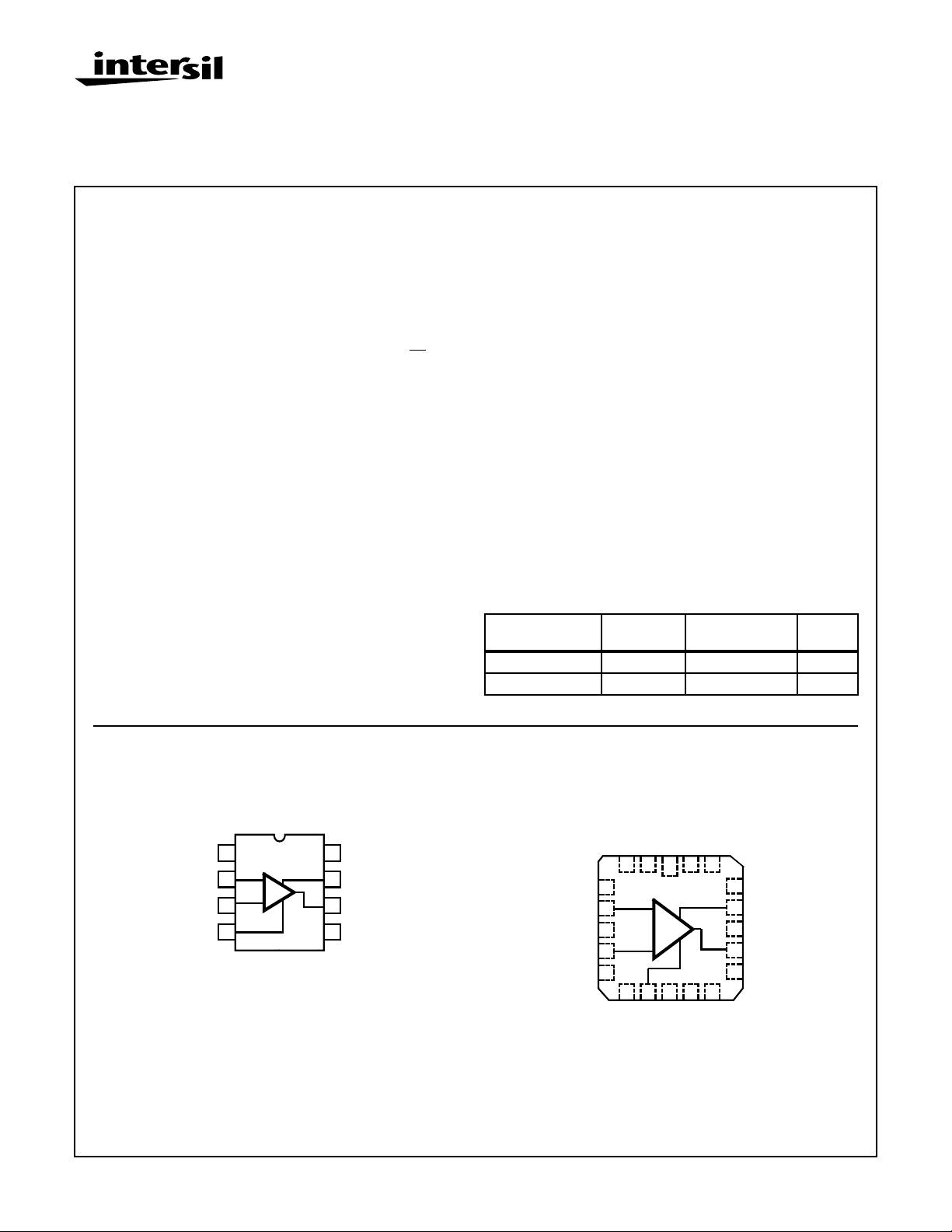
Ordering Information
TEMP.
PART NUMBER
HA4-5147/883 -55 to 125 20 Ld CLCC J20.A
HA7-5147/883 -55 to 125 8 Ld CERDIP F8.3A
RANGE (oC) PACKAGE
PKG.
NO.
,
Pinouts
HA-5147/883
(CERDIP)
TOP VIEW
1
BAL
-IN
2
-
+IN
V-
CAUTION: These devices are sensitive to electrostatic discharge; follow proper IC Handling Procedures.
1-888-INTERSIL or 321-724-7143
+
3
4
| Copyright © Intersil Corporation 1999
8
BAL
7
V+
6
OUT
NC
5
1
NC
-IN
NC
+IN
NC
HA-5147/883
(CLCC)
TOP VIEW
NC
BALNCNC
3212019
4
5
6
7
8
+
9101112
NCV-NC
BAL
18
NC
V+
17
16
NC
OUT
15
NC
14
13
NC
NC
Spec Number 511009-883
File Number 3715.2
Page 2
HA-5147/883
Absolute Maximum Ratings Thermal Information
Voltage Between V+ and V- Terminals. . . . . . . . . . . . . . . . . . . . 44V
Differential Input Voltage (Note 1). . . . . . . . . . . . . . . . . . . . . . . .0.7V
Voltage at Either Input Terminal . . . . . . . . . . . . . . . . . . . . . . V+ to V-
Input Current. . . . . . . . . . . . . . . . . . . . . . . . . . . . . . . . . . . . . . .25mA
Output Current . . . . . . . . . . . . . . . . . . . Full Short Circuit Protection
ESD Rating. . . . . . . . . . . . . . . . . . . . . . . . . . . . . . . . . . . . . . <2000V
Operating Conditions
Temperature Range . . . . . . . . . . . . . . . . . . . . . . . . . -55oC to 125oC
Supply Voltage . . . . . . . . . . . . . . . . . . . . . . . . . . . . . . . . . . . . . . . . . ±15V
V
≤ 1/2 (V+ - V-)
INCM
RL≥ 600Ω
CAUTION: Stresses above those listed in “Absolute Maximum Ratings” may cause permanent damage to the device. This is a stress only rating and operation
of the device at these or any other conditions above those indicated in the operational sections of this specification is not implied.
NOTES:
1. For differential input voltages greater than 0.7V, the input current must be limited to 25mA to protect the back-to-back input diodes.
2. θJA is measured with the component mounted on an evaluation PC board in free air.
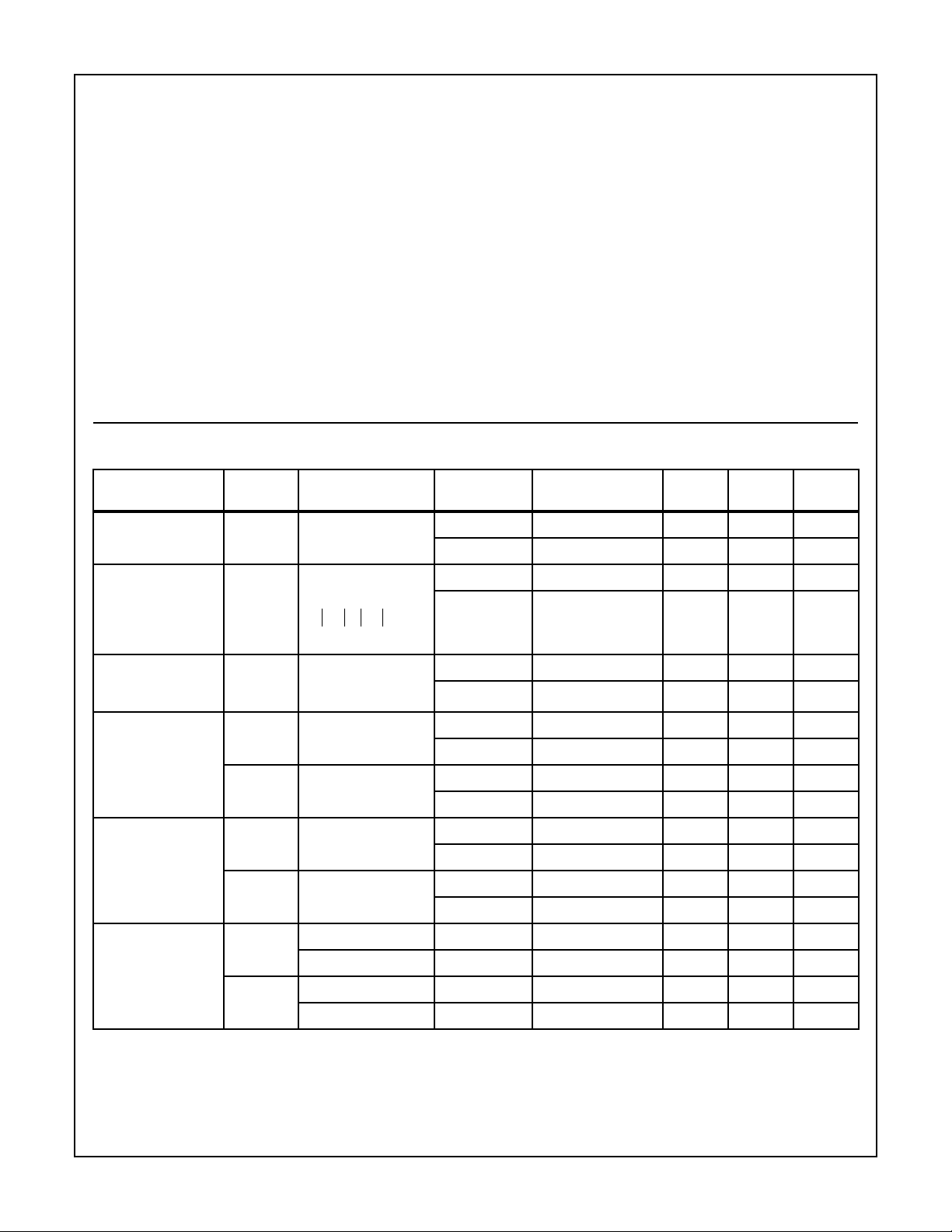
TABLE 1. DC ELECTRICAL PERFORMANCE SPECIFICATIONS
Device Tested at: V
PARAMETER SYMBOL CONDITIONS
Input Offset Voltage V
Input Bias Current I
SUPPLY
= ±15V, R
IO
B
SOURCE
= 50Ω, R
LOAD
= 100kΩ, V
VCM = 0V 1 25 -100 100 µV
VCM = 0V,
RS = 10kΩ, 50Ω
+I
+
BI–B
------------------------------
2
Thermal Resistance (Typical, Note 2) θJA (oC/W) θJC (oC/W)
CERDIP Package . . . . . . . . . . . . . . . . 115 28
CLCC Package . . . . . . . . . . . . . . . . . . 65 15
Package Power Dissipation Limit at 75oC for TJ≤ 175oC
CERDIP Package . . . . . . . . . . . . . . . . . . . . . . . . . . . . . . . 870mW
CLCC Package . . . . . . . . . . . . . . . . . . . . . . . . . . . . . . . . . .1.54W
Package Power Dissipation Derating Factor Above 75oC
CERDIP Package . . . . . . . . . . . . . . . . . . . . . . . . . . . . .8.7mW/oC
CLCC Package . . . . . . . . . . . . . . . . . . . . . . . . . . . . . .15.4mW/oC
Maximum Junction Temperature (TJ) . . . . . . . . . . . . . . . . . . . 175oC
Maximum Storage Temperature Range . . . . . . . . . .-65oC to 150oC
Maximum Lead Temperature (Soldering 10s) . . . . . . . . . . . . . 300oC
= 0V, Unless Otherwise Specified.
OUT
GROUP A
SUBGROUPS TEMP. (oC) MIN MAX UNITS
2, 3 125, -55 -300 300 µV
1 25 - 80 nA
2, 3 125, -55 - 150 nA
Input Offset Current I
Common Mode
+CMR V+ = +4.7V,
Range
Large Signal Voltage
+A
Gain
Common Mode
+CMRR ∆VCM = +11V 1 25 100 - dB
Rejection Ratio
-CMRR ∆VCM = -11V 1 25 100 - dB
VCM = 0V,
IO
+RS = 10kΩ,
-RS = 10kΩ
V- = -25.3V
-CMR V+ = +25.3V,
V- = -4.7V
V
VOL
= 0V and +10V,
OUT
RL = 2kΩ
-A
VOL
V
= 0V and -10V,
OUT
RL = 2kΩ
∆VCM = +10V 2, 3 125, -55 100 - dB
∆VCM = -10V 2, 3 125, -55 100 - dB
1 25 -75 75 nA
2, 3 125, -55 -135 135 nA
1 25 10.3 - V
2, 3 125, -55 10.3 - V
1 25 - -10.3 V
2, 3 125, -55 - -10.3 V
4 25 700 - kV/V
5, 6 125, -55 300 - kV/V
4 25 700 - kV/V
5, 6 125, -55 300 - kV/V
Spec Number 511009-883
2
Page 3
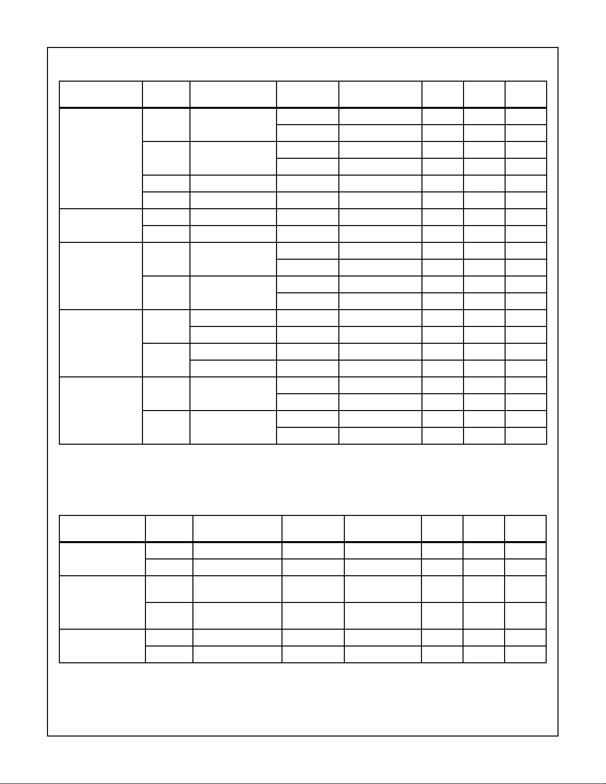
TABLE 1. DC ELECTRICAL PERFORMANCE SPECIFICATIONS (Continued)
Device Tested at: V
SUPPLY
= ±15V, R
SOURCE
PARAMETER SYMBOL CONDITIONS
= 50Ω, R
HA-5147/883
= 100kΩ, V
LOAD
GROUP A
SUBGROUPS TEMP. (oC) MIN MAX UNITS
= 0V, Unless Otherwise Specified.
OUT
Output Voltage Swing +V
OUT1RL
= 2kΩ 4 25 11.5 - V
5, 6 125, -55 11.5 - V
-V
OUT1RL
= 2kΩ 4 25 - -11.5 V
5, 6 125, -55 - -11.5 V
+V
-V
Output Current +I
Quiescent Power
Supply Current
OUT2RL
OUT2RL
OUT
-I
OUT
+I
CC
-I
CC
= 600Ω 42510-V
= 600Ω 4 25 - -10 V
V
= -10V 4 25 16.5 - mA
OUT
V
= +10V 4 25 - -16.5 mA
OUT
V
OUT
=0V,I
= 0mA 1 25 - 4 mA
OUT
2, 3 125, -55 - 4 mA
V
OUT
=0V,I
= 0mA 1 25 -4 - mA
OUT
2, 3 125, -55 -4 - mA
Power Supply
Rejection Ratio
Offset Voltage
Adjustment
+PSRR ∆V
-PSRR ∆V
= +14V 1 25 86 - dB
SUP
∆V
= +13.5V 2, 3 125, -55 86 - dB
SUP
= +14V 1 25 86 - dB
SUP
∆V
= +13.5V 2, 3 125, -55 86 - dB
SUP
+VIOAdj Note 3 1 25 VIO-1 - mV
2, 3 125, -55 VIO-1 - mV
-VIOAdj Note 3 1 25 VIO+1 - mV
2, 3 125, -55 VIO+1 - mV
NOTE:
3. Offset adjustment range is [VIO(Measured) ±1mV] minimum referred to output. This test is for functionality only to assure adjustment
through 0V.
TABLE 2. AC ELECTRICAL PERFORMANCE SPECIFICATIONS
Device Tested at: V
SUPPLY
= ±15V, R
SOURCE
PARAMETER SYMBOL CONDITIONS
Slew Rate +SR V
-SR V
Rise and Fall Time t
r
= -3V to +3V 7 25 28 - V/µs
OUT
= +3V to -3V 7 25 28 - V/µs
OUT
V
= 0 to +200mV
OUT
10% ≤ tr≤ 90%
t
V
f
= 0 to -200mV
OUT
10% ≤ tf≤ 90%
Overshoot +OS V
-OS V
= 0 to +200mV 7 25 - 40 %
OUT
= 0 to -200mV 7 25 - 40 %
OUT
= 50Ω, R
LOAD
= 2kΩ, C
LOAD
= 50pF, A
= +10V/V, Unless Otherwise Specified.
VCL
GROUP A
SUBGROUPS TEMP. (oC) MIN MAX UNITS
7 25 - 50 ns
7 25 - 50 ns
Spec Number 511009-883
3
Page 4

HA-5147/883
TABLE 3. ELECTRICAL PERFORMANCE SPECIFICATIONS
Device Characterized at: V
PARAMETER SYMBOL CONDITIONS NOTES TEMP. (oC) MIN MAX UNITS
SUPPLY
= ±15V, R
LOAD
= 2kΩ, C
= 50pF, AV = +10V/V, Unless Otherwise Specified.
LOAD
Average Offset Voltage
VIOTC VCM = 0V 4 -55 to 125 - 1.8 µV/oC
Drift
Differential Input
R
VCM = 0V 4 25 0.8 - MΩ
IN
Resistance
Low Frequency
E
NP-P
0.1Hz to 10Hz 4 25 - 0.25 µV
P-P
Peak-to-Peak Noise
Input Noise Voltage
Density
E
RS = 20Ω, fO = 10Hz 4 25 - 10 nV/√Hz
N
RS = 20Ω, fO = 100Hz 4 25 - 5.6 nV/√Hz
RS = 20Ω, fO = 1kHz 4 25 - 4.5 nV/√Hz
Input Noise Current
Density
I
RS = 2MΩ, fO = 10Hz 4 25 - 4.0 pA/√Hz
N
RS = 2MΩ, fO = 100Hz 4 25 - 2.3 pA/√Hz
RS = 2MΩ, fO = 1kHz 4 25 - 0.6 pA/√Hz
Gain Bandwidth Product GBWP VO= 100mV, fO=10kHz 4 25 120 - MHz
VO= 100mV, fO=1MHz 4 25 100 - MHz
Full Power Bandwidth FPBW V
Minimum Closed Loop
CLSG RL = 2kΩ, CL = 50pF 4 -55 to 125 ±10 - V/V
= 10V 4, 5 25 445 - kHz
PEAK
Stable Gain
Settling Time t
Output Resistance R
Quiescent Power
OUT
PC V
To 0.1% for a 10V Step 4 25 - 600 µs
S
Open Loop 4 25 - 100 Ω
OUT
=0V,I
= 0mA 4, 6 -55 to 125 - 120 mW
OUT
Consumption
NOTES:
4. Parameters listed in Table 3 are controlled via design or process parameters and are not directly tested at final production. These parameters are lab characterized upon initial design release, or upon design changes. These parameters are guaranteed by characterization based upon data from multiple production runs which reflect lot to lot and within lot variation.
5. Full Power Bandwidth guarantee based on Slew Rate measurement using FPBW = Slew Rate/(2πV
PEAK
).
6. Quiescent Power Consumption based upon Quiescent Supply Current test maximum. (No load on output.)
TABLE 4. ELECTRICAL TEST REQUIREMENTS
MIL-STD-883 TEST REQUIREMENTS SUBGROUPS (SEE TABLES 1 AND 2)
Interim Electrical Parameters (Pre Burn-In) 1
Final Electrical Test Parameters 1 (Note 7), 2, 3, 4, 5, 6, 7
Group A Test Requirements 1, 2, 3, 4, 5, 6, 7
Groups C and D Endpoints 1
NOTE:
7. PDA applies to Subgroup 1 only.
4
Spec Number 511009-883
Page 5

Die Characteristics
HA-5147/883
DIE DIMENSIONS:
104.3 x 65 x 19 mils
2650 x 1650 x 483µm
METALLIZATION:
Type: Al, 1% Cu
Thickness: 16k
Å ± 2kÅ
GLASSIVATION:
Type: Nitride (Si
) over Silox (SiO2, 5% Phos.)
3N4
Silox Thickness: 12kÅ ± 2kÅ
Nitride Thickness: 3.5kÅ ± 1.5kÅ
Metallization Mask Layout
BAL
WORST CASE CURRENT DENSITY:
3.6 x 10
5
A/cm2at 15mA
This de vice meets Glassiv ation Integrity Test Requirement
per MIL-STD-883 Method 2021 and MIL-I-38535 Paragraph
30.5.5.4.
SUBSTRATE POTENTIAL (Powered Up):
V-
TRANSISTOR COUNT:
63
PROCESS:
Bipolar Dielectric Isolation
HA-5147/883
BAL
-IN
+IN
V+
OUT
V-
NC
Spec Number 511009-883
5
Page 6

Burn-In Circuits
HA-5147/883
HA-5147/883 CERDIP
R
2
R
1
V-
D
2
C
2
1
2
-
+
3
4
R
3
8
7
C
6
5
1
V+
D
1
HA-5147/883 CLCC
R
2
32120 19
R
1
R
4
5
6
7
8
3
-
+
9 10111213
18
17
C
16
15
14
1
V+
D
1
NOTE:
R1 = R3 = 1kΩ, ±5%,1/4W (Min.)
R2 = 10kΩ, ±5%,1/4W (Min.)
C1 = C2 = 0.01µF/Socket or 0.1µF/Row (Min.)
D1 = D2 = 1N4002 or Equivalent/Board
|(V+) - (V-)| = 30V
C
2
V-
D
2
Spec Number 511009-883
6
Page 7

HA-5147/883
Typical Performance Information T
= 25oC, V
A
R
1
2
3
4
T
-
+
10kΩ
= ±15V, Unless Otherwise Specified
SUPPLY
V+
8
7
6
5
NOTE: Tested offset adjustment range is |VOS±1mV| minimum referred to output. Typical range is ±4mV with RT = 10kΩ.
SUGGESTED OFFSET VOLTAGE ADJUSTMENT
AV = +10V/V
V
AC
50Ω
+
-
1.8kΩ
50pF
V
OUT
AC
OUT
200Ω
LARGE AND SMALL SIGNAL RESPONSE TEST CIRCUIT
IN
IN
OUT
Vertical Scale: Input = 0.5V/Div.
Output = 5V/Div.
Horizontal Scale: 500ns/Div.
LARGE SIGNAL RESPONSE
Vertical Scale: Input = 10mV/Div.
Output = 100mV/Div.
Horizontal Scale: 100ns/Div.
SMALL SIGNAL RESPONSE
Spec Number 511009-883
7
Page 8

HA-5147/883
Ceramic Leadless Chip Carrier Packages (CLCC)
j x 45
E1
o
B
h x 45
-E-
E2
e1
o
A
-F-
0.010 E HS S
L
D
D3
0.007 E FM S HS
B1
L2
D1
-H-
D2
B2
J20.A MIL-STD-1835 CQCC1-N20 (C-2)
20 PAD CERAMIC LEADLESS CHIP CARRIER PACKAGE
INCHES MILLIMETERS
SYMBOL
A 0.060 0.100 1.52 2.54 6, 7
A1 0.050 0.088 1.27 2.23 -
B-----
B1 0.022 0.028 0.56 0.71 2, 4
E3
E
B2 0.072 REF 1.83 REF B3 0.006 0.022 0.15 0.56 -
D 0.342 0.358 8.69 9.09 D1 0.200 BSC 5.08 BSC D2 0.100 BSC 2.54 BSC D3 - 0.358 - 9.09 2
0.010 E FSS
A1
E 0.342 0.358 8.69 9.09 E1 0.200 BSC 5.08 BSC E2 0.100 BSC 2.54 BSC -
PLANE 2
PLANE 1
E3 - 0.358 - 9.09 2
e 0.050 BSC 1.27 BSC e1 0.015 - 0.38 - 2
h 0.040 REF 1.02 REF 5
j 0.020 REF 0.51 REF 5
L 0.045 0.055 1.14 1.40 L1 0.045 0.055 1.14 1.40 -
e
L3
L2 0.075 0.095 1.91 2.41 L3 0.003 0.015 0.08 0.38 -
ND 5 5 3
NE 5 5 3
N20 203
B3
NOTES:
1. Metallized castellations shall be connected to plane 1 terminals
and extend toward plane 2 across at least two layers of ceramic
or completely across all of the ceramic layers to make electrical
connection with the optional plane 2 terminals.
2. Unless otherwise specified, a minimum clearance of 0.015 inch
(0.38mm) shall be maintained between all metallized features
L1
(e.g., lid, castellations, terminals, thermal pads, etc.)
3. Symbol “N” is the maximum number of terminals. Symbols “ND”
and “NE” are the number of terminals along the sides of length
“D” and “E”, respectively.
4. The required plane 1 terminals and optional plane 2 terminals (if
used) shall be electrically connected.
5. The corner shape (square, notch, radius, etc.) may vary at the
manufacturer’s option, from that shown on the drawing.
6. Chip carriers shall be constructed of a minimum of two ceramic
layers.
7. Dimension “A” controls the overall package thickness . The maximum “A” dimension is package height before being solder dipped.
8. Dimensioning and tolerancing per ANSI Y14.5M-1982.
9. Controlling dimension: INCH.
NOTESMIN MAX MIN MAX
Rev. 0 5/18/94
Spec Number 511009-883
8
Page 9

HA-5147/883
Ceramic Dual-In-Line Frit Seal Packages (CERDIP)
c1
LEAD FINISH
-DBASE
M
SECTION A-A
METAL
b1
M
(b)
α
E
D
S
S
Q
A
-CL
eA
eA/2
aaa C A - B
M
c
S
bbb C A - B
BASE
PLANE
SEATING
PLANE
S1
b2
b
ccc C A - BMD
-A-
-B-
S
D
A
A
e
S
S
NOTES:
1. Index area:A notch or apin one identificationmark shall be located adjacent to pin one and shall be located within the shaded
area shown. The manufacturer’s identification shall not be used
as a pin one identification mark.
2. The maximum limits of lead dimensions b and c or M shall be
measured at the centroid of the finished lead surfaces, when
solder dip or tin plate lead finish is applied.
3. Dimensions b1 and c1 apply to lead base metal only. Dimension
M applies to lead plating and finish thickness.
4. Corner leads (1, N, N/2, and N/2+1) may be configured with a
partial lead paddle. For this configuration dimension b3 replaces
dimension b2.
5. This dimension allows for off-center lid, meniscus, and glass
overrun.
6. Dimension Q shall be measured from the seating plane to the
base plane.
7. Measure dimension S1 at all four corners.
8. N is the maximum number of terminal positions.
9. Dimensioning and tolerancing per ANSI Y14.5M - 1982.
10. Controlling dimension: INCH
D
F8.3A MIL-STD-1835 GDIP1-T8 (D-4, CONFIGURATION A)
8 LEAD CERAMIC DUAL-IN-LINE FRIT SEAL PACKAGE
(c)
SYMBOL
S
eA 0.300 BSC 7.62 BSC -
eA/2 0.150 BSC 3.81 BSC -
S1 0.005 - 0.13 - 7
aaa - 0.015 - 0.38 bbb - 0.030 - 0.76 -
ccc - 0.010 - 0.25 -
INCHES MILLIMETERS
NOTESMIN MAX MIN MAX
A - 0.200 - 5.08 -
b 0.014 0.026 0.36 0.66 2
b1 0.014 0.023 0.36 0.58 3
b2 0.045 0.065 1.14 1.65 b3 0.023 0.045 0.58 1.14 4
c 0.008 0.018 0.20 0.46 2
c1 0.008 0.015 0.20 0.38 3
D - 0.405 - 10.29 5
E 0.220 0.310 5.59 7.87 5
e 0.100 BSC 2.54 BSC -
L 0.125 0.200 3.18 5.08 -
Q 0.015 0.060 0.38 1.52 6
o
α
90
105
o
90
o
105
o
-
M - 0.0015 - 0.038 2, 3
N8 88
Rev. 0 4/94
All Intersil semiconductor products are manufactured, assembled and tested under ISO9000 quality systems certification.
Intersil products are sold by description only. Intersil Corporation reserves the right to make changes in circuit design and/or specifications at any time without notice.
Accordingly ,the reader is cautioned to verify that data sheets are current before placing orders. Information furnished by Intersil is believed to be accurate and reliable. However, no responsibility is assumed by Intersil or its subsidiaries for its use; nor for any infringements of patents or other rights of third parties which may
result from its use. No license is granted by implication or otherwise under any patent or patent rights of Intersil or its subsidiaries.
For information regarding Intersil Corporation and its products, see web site http://www.intersil.com
Sales Office Headquarters
NORTH AMERICA
Intersil Corporation
P. O. Box 883, Mail Stop 53-204
Melbourne, FL 32902
TEL: (321) 724-7000
FAX: (321) 724-7240
EUROPE
Intersil SA
Mercure Center
100, Rue de la Fusee
1130 Brussels, Belgium
TEL: (32) 2.724.2111
FAX: (32) 2.724.22.05
ASIA
Intersil (Taiwan) Ltd.
Taiwan Limited
7F-6, No. 101 Fu Hsing North Road
Taipei, Taiwan
Republic of China
TEL: (886) 2 2716 9310
FAX: (886) 2 2715 3029
Spec Number 511009-883
9
 Loading...