

Page 1

Semiconductor
HA-5004
OBSOLETE PRODUCT
NO RECOMMENDED REPLACEMENT
Call Central Applications 1-800-442-7747
or email: centapp@harris.com
100MHz Current Feedback Amplifier
The HA-5004 current feedbackamplifierisavideo/wideband
amplifier optimized for low gain applications. The design is
based on current-mode feedback which allows the amplifier
to achieve higher closed loop bandwidth than voltage-mode
feedback operational amplifiers. Since feedback is
employed, the HA-5004 can offer better gain accuracy and
lower distortion than open loop buffers. Unlike conventional
op amps, the bandwidth and rise time of the HA-5004 are
nearly independent of closed loop gain. The 100MHz
bandwidth at unity gain reduces to only 65MHz at a gain of
10. The HA-5004 may be used in place of a conventional op
amp with a significant improvement in speed power product.
Several features have been designed in for added value. A
thermal overload feature protects the part against excessive
junction temperature by shutting down the output. If this
feature is not needed, it can be inhibited via a TTL input
(TOI).ATTLchipenable/disable(
the chip is disabled its output is high impedance. Finally, an
open collector output flag (
status of the chip. The status flag goes low to indicate when
the chip is disabled due to either the internal Thermal
Overload shutdown or the external disable.
In order to maximize bandwidth and output drive capacity,
internal current limiting is not provided. However, current
limiting may be applied via the V
provide power separately to the output stage.
OE) is also provided; when
TOL) is provided to indicate the
+ and VC- pins which
C
January 1999 File Number 2923.4
Features
• Slew Rate. . . . . . . . . . . . . . . . . . . . . . . . . . . . . . 1200V/µs
• Output Current . . . . . . . . . . . . . . . . . . . . . . . . . . .
• Drives. . . . . . . . . . . . . . . . . . . . . . . . . . . . .
•V
SUPPLY
. . . . . . . . . . . . . . . . . . . . . . . . . . . . . ±5V to ±18V
±100mA
±9V into 100Ω
• Thermal Overload Protection and Output Flag
• Bandwidth Nearly Independent of Gain
• Output Enable/Disable
Applications
• Unity Gain Video/Wideband Buffer
• Video Gain Block
• High Speed Peak Detector
• Fiber Optic Transmitters
• Zero Insertion Loss Transmission Line Drivers
• Current to Voltage Converter
• Radar Systems
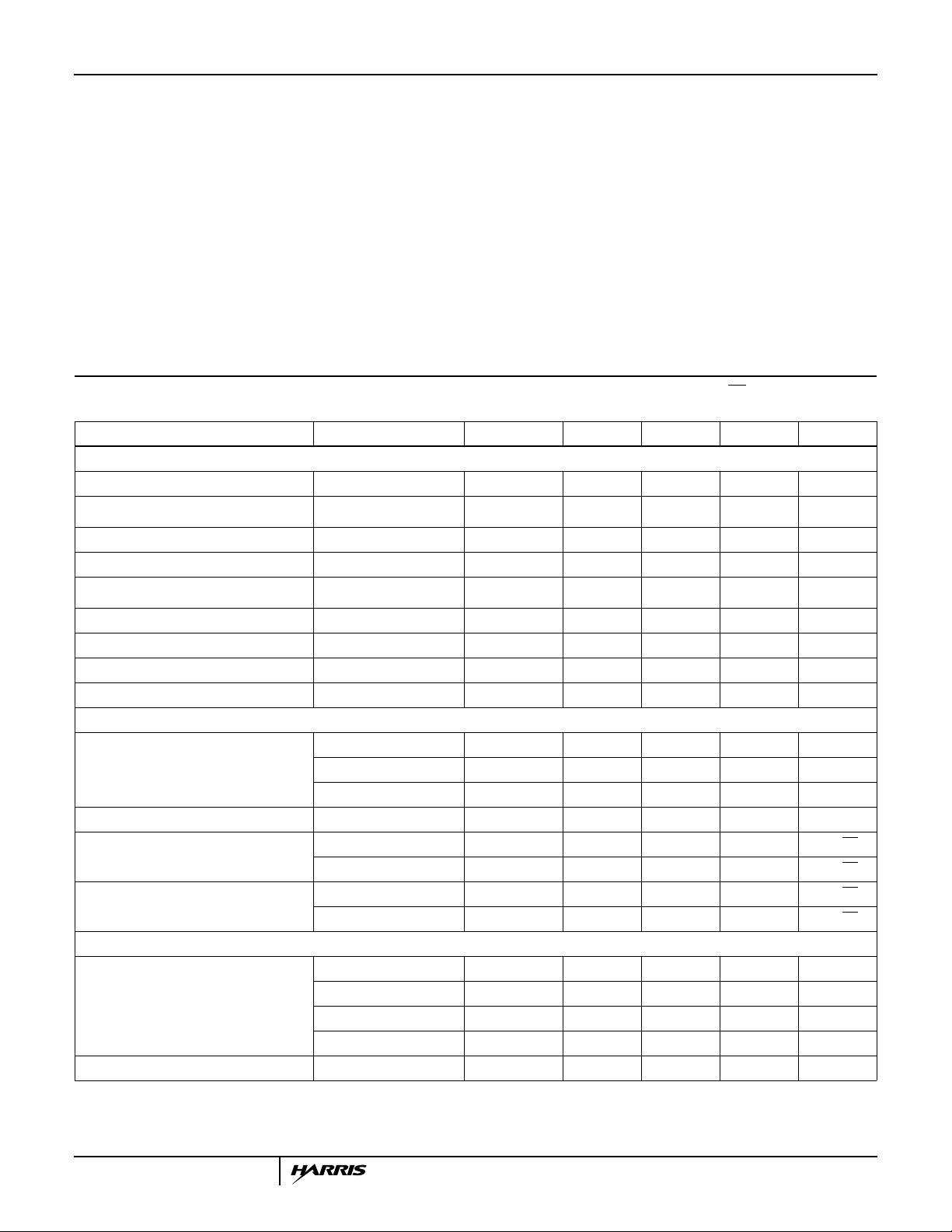
Part Number Information
TEMP.
PART NUMBER
HA1-5004-5 0 to 70 14 Ld CERDIP F14.3
RANGE (oC) PACKAGE PKG. NO.
For Military grade product refer to the HA-5004/883 data
sheet.
Pinout
HA-5004
(CERDIP)
TOP VIEW
V
OUT
+BAL
-BAL
V
CC
TOI
OE
C+
1
2
3
4
5
6
7
-
+
1
V
14
C-
V
13
EE
-IN
12
+IN
11
TOL
10
GND
9
N/C
8
CAUTION: These devices are sensitive to electrostatic discharge; follow proper IC Handling Procedures.
TRUTH TABLE
INPUTS TEMP TOL OUTPUT
(OPEN
COLLECTOR) OPERATIONOE TOI T
J
0 0 Normal 1 Normal
0 0 High
(Note)
0 1 X 1 Normal
1 X X 0 Manual Shutdown,
NOTE: >180oC Typical
1-800-4-HARRIS or 407-727-9207 | Copyright
0 Auto Shutdown,
HI-Z OUT
HI-Z OUT
© Harris Corporation 1999
Page 2
HA-5004
Absolute Maximum Ratings Thermal Information
Supply Voltage (Between V+ and V- Terminals) . . . . . . . . . . . . 40V
Differential Input Voltage . . . . . . . . . . . . . . . . . . . . . . . . . . . . . . . 5V
DC Input Voltage . . . . . . . . . . . . . . . . . . . . . . . . . . . . . . . ±V
Output Current. . . . . . . . . . . . . . . ±120mA Max (≤25% Duty Cycle)
SUPPLY
Operating Conditions
Temperature Range
HA-5004-5 . . . . . . . . . . . . . . . . . . . . . . . . . . . . . . . . 0oC to 75oC
CAUTION: Stresses above those listed in “Absolute Maximum Ratings” may cause permanent damage to the device. This is a stress only rating and operationofthe
device at these or any other conditions above those indicated in the operational sections of this specification is not implied.
NOTES:
1. Maximum power dissipation, including load condition, must be designed to maintain the junction temperature below 175oC. See Thermal Resistances in the “Thermal Information” section.
2. θJA is measured with the component mounted on an evaluation PC board in free air.
Thermal Resistance (Typical, Note 2) θJA (oC/W) θJC (oC/W)
CERDIP Package. . . . . . . . . . . . . . . . . 75 20
Maximum Junction Temperature (Note 1) . . . . . . . . . . . . . . . 175oC
Maximum Storage Temperature Range. . . . . . . . . . -65oC to 150oC
Maximum Lead Temperature (Soldering 10s) . . . . . . . . . . . . 300oC
Electrical Specifications V
PARAMETER TEST CONDITIONS TEMP. (oC) MIN TYP MAX UNITS
INPUT CHARACTERISTICS
Offset Voltage 25 - 1 5 mV
Average Offset Voltage Drift Full - 10 - µV/oC
Bias Current (+Input Only) (Note 3) 25 - 2 5 µA
Input Resistance (-Input) 25 - 6.5 - Ω
Input Resistance (+Input) 25 - 3 - MΩ
Input Capacitance 25 - 3 - pF
Common Mode Range Full ±10 - - V
DISTORTION AND NOISE
Total Harmonic Distortion (2V
200kHz)
Input Noise Voltage 10Hz to 1MHz 25 - 15 - µV
Input Noise Voltage Density (Note 4) f = 10kHz 25 - 2.2 - nV/√Hz
Input Noise Current Density (Note 4) f = 10kHz 25 - 6 - pA/√Hz
DIGITAL I/O CHARACTERISTICS
Logic Inputs (OE and TO) V
Logic Output (TOL) (Open Collector) VOL at 800µA Full - 0.05 0.4 V
P-P
= VC+ = +15V, VEE = VC- = -15V, RS = 50Ω, RL = 100Ω, AV = +1, RF = 250Ω, OE = 0.8V, TOI = 0.8V or
CC
2.0V, Unless Otherwise Specified
Full - - 20 mV
Full - - 20 µA
,
A
= +1 25 - -72 - dBc
VCL
A
= +2 25 - -70 - dBc
VCL
A
= +5 25 - -68 - dBc
VCL
f = 100kHz 25 - 2.2 - nV/√Hz
f = 100kHz 25 - 4 - pA/√Hz
IH
V
IL
IIH at VI = 2.4V Full - - 1 µA
IIH at VI = 0.4V Full - - 10 µA
Full 2.0 - - V
Full - - 0.8 V
P-P
2
Page 3
HA-5004
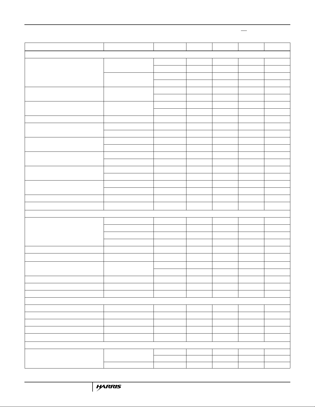
Electrical Specifications V
= VC+ = +15V, VEE = VC- = -15V, RS = 50Ω, RL = 100Ω, AV = +1, RF = 250Ω, OE = 0.8V, TOI = 0.8V or
CC
2.0V, Unless Otherwise Specified (Continued)
PARAMETER TEST CONDITIONS TEMP. (oC) MIN TYP MAX UNITS
TRANSFER CHARACTERISTICS
DC Gain Error (Note 5) Small Signal
(±100mV)
Large Signal (±10V)
(RL = 1kΩ)
25 - 0.25 0.43 %
Full - 0.25 0.75 %
25 - 0.25 0.43 %
Full - 0.25 0.75 %
DC Voltage Gain Small and Large Signal 25 233 400 - V/V
Full 133 400 - V/V
DC Transimpedance (Note 6) 25 - 100 - V/mA
Full 33 100 - V/mA
-3dB Bandwidth (Note 7) AV = +1 25 - 100 - MHz
Gain Flatness DC to 5MHz 25 - 0.03 - dB
DC to 10MHz 25 - 0.05 - dB
Differential Gain (Notes 7, 8, 9, 3.58MHz) A
Differential Gain (Notes 7, 8, 9, 4.43MHz) A
Differential Phase (Notes 7, 8, 3.58MHz) A
Differential Phase (Notes 7, 8, 4.43MHz) A
= +1 25 - 0.035 - %
VCL
A
= +2 25 - 0.058 - %
VCL
= +1 25 - 0.035 - %
VCL
A
= +2 25 - 0.058 - %
VCL
= +1 25 - 0.15 - Degrees
VCL
A
= +2 25 - 0.23 - Degrees
VCL
= +1 25 - 0.17 - Degrees
VCL
A
= +2 25 - 0.24 - Degrees
VCL
Common Mode Rejection Ratio VCM = ±10V Full - 58 - dB
Minimum Stable Gain Full 1 - - V/V
OUTPUT CHARACTERISTICS
Output Voltage Swing RL = 100Ω 25 ±9.0 ±9.5 - V
RL = 1kΩ 25 ±11.5 ±11.8 - V
RL = 100Ω Full ±8.0 ±9.5 - V
RL = 1kΩ Full ±10.5 ±11.8 - V
Full Power Bandwidth AV = +1, V
OUT
= 4V
P-P
25 - 50 - MHz
Output Resistance, Open Loop 25 - 5 - Ω
Output Current 25 ±90 ±100 - mA
Full ±80 ±100 - mA
Output Enable Time HI-Z to ±2V Full - 100 - ns
Output Disable Time ±2V to HI-Z Full - 3 - µs
Output Leakage Disabled Full - - 1 µA
TRANSIENT RESPONSE
Rise Time/Fall Time 200mV Step 25 - 6.3 - ns
Propagation Delay 10V Step 25 - 7 - ns
Slew Rate 10V Step 25 - 1200 - V/µs
Settling Time 0.1%, 10V Step 25 - 50 - ns
Overshoot 25 - 10 - %
POWER SUPPLY CHARACTERISTICS
Supply Current Enabled 25 - 12 16 mA
Full - - 22 mA
Disabled 25 - 7 - mA
3
Page 4

HA-5004
Electrical Specifications V
= VC+ = +15V, VEE = VC- = -15V, RS = 50Ω, RL = 100Ω, AV = +1, RF = 250Ω, OE = 0.8V, TOI = 0.8V or
CC
2.0V, Unless Otherwise Specified (Continued)
PARAMETER TEST CONDITIONS TEMP. (oC) MIN TYP MAX UNITS
Power Supply Rejection Ratio Full 50 60 - dB
NOTES:
3. The inverting input is a low impedance point; Bias Current and Offset Current, are not specified for this terminal.
4. See typical performance curves.
1
5. .
Gain Error
6. .
DC Transimpedance
7. VIN = 300mV
8. V
OFFSET
-------------------------------------------- -
DC Voltage Gain
P-P.
= 1.0V.
R
F
---------------------------
Gain Error
100%×=
,RF250Ω==
9. Differential Gain (dB) = 0.0869 Differential Gain (%).
Test Circuits and Waveforms
INPUT
V
IN
+
-
V
OUT
OUTPUT
INPUT
OUTPUT
AV = +1, V
SUPPLY
= ±15V
Vertical Scale: 5V/Div.; Horizontal Scale: 20ns/Div.
LARGE SIGNAL RESPONSE, AV = +1
AV = +1, V
SUPPLY
= ±15V
Vertical Scale: 2V/Div.; Horizontal Scale: 20ns/Div.
INPUT
OUTPUT
249Ω
FIGURE 1. TEST CIRCUIT
A
= +1, V
V
SUPPLY
= ±15V
Vertical Scale: 100mV/Div.; Horizontal Scale: 20ns/Div.
PROPAGATION DELAY SMALL SIGNAL RESPONSE
4
Page 5

HA-5004
OETOL
C+
V
CC
V
BAL 2
BAL1
R
24A
XU2
R
R
R
R
R
R
R
R
R
R
R
R
R
R
R
R
R
R
R
R
5
32
4
26
3
31
24B
29
30
23
25
T12
T15
T13
T8
T9
T16
T5
T4
35
N7
R
Q
P5
Q
R
P4
Q
D1
D
D2
D
P3
Q
N30
Q
P
Q
31
P24
Q
P32
Q
N26
Q
P22
Q
N25
Q
NT9
Q
PT12
Q
PT18
Q
PT13
Q
NT12
Q
PT10
Q
PT17
Q
PT3
Q
PT2
Q
34B
R
34A
N2
Q
Q
Q
NT10
Q
NT11
Q
PT11
Q
Q
P23
N20
P1
D
Q
D7
PT4
OUT
P6
Q
FB
IN
XU9
R
20
R
D
Q
Q
Q
R
D8
N6B
N6A
D6
D
N1
Q
N
Q
T10
N21
37
P7
R
Q
36B
R
36A
N5
Q
Q
Q
N3
P30
Q
P28
Q
P25
Q
R
R
R
R
N31
R
N4
C1
Q
C
D4
D
D3
D
P2
Q
D8
D
N24
Q
N32
Q
23
N22
Q
Z1
D
8
7
27
6
22B
R
22A
R
28
R
21
R
C-
V
EE
V
GND
PT14
Q
T14
R
PT15
R
T18
R
T19
NT4
Q
Q
PT6
Q
PT9
Q
T6
R
NT3
NT2
Q
Q
ZT1
D
ZT2
D
Q
NT8
Q
NT7
T1
R
T1
R
Schematic Diagram
PT1
Q
T7
R
T17
TOI
R
Q
PT7
R
T20
Q
Q
PT5
PT6
NT6
Q
Q
NT5
5
Page 6

HA-5004
Application Information
Theory Of Operation
The HA-5004 is a high performance amplifier that uses
current feedback to achieve its outstanding performance.
Although it is externally configured like an ordinary op amp
in most applications, its internal operation is significantly
different.
Inside the HA-5004, there is a unity gain buffer from the noninverting (+) input to the inverting-input (as suggested by the
circuit symbol), and the inverting terminal is a low
impedance point. Error currents are sensed at the inverting
input and amplified; a small change in input current
produces a large change in output voltage. The ratio of
output voltage delta due to input current delta is the
transimpedance of the device.
Steady state current at the inverting input is very small
because the transimpedance is large. The voltage across
the input terminals is nearly zero due to the buffer amplifier.
These two properties are similar to standard op amps and
likewise simplify circuit analysis.
Resistor Selection
The HA-5004 is optimized for a feedback resistor of 250Ω,
regardless of gain configuration. It is important to note that
this resistor is required even for unity gain applications;
higher gain settings use a second resistor like regular op
amp circuits as shown in Figure 2 below.
+5V
Ω
10k
THERMAL OVERLOAD
8
NC
9
GND
10
TOL
V
IN
-15V
249Ω
100
11
+
-
12
13
V
EE
14
V
C-
R
249Ω
7
OE
6
TOI
5
V
CC
-
5kΩ
4
BAL
3
+
2
Ω
C+
100
1
+15V
V
F
V
OUT
capacitors from each supply to ground are recommended,
typically a 0.01
µF ceramic in parallel with a 4.7µF
electrolytic.
Current Limit
No internal current limiting is provided for the HA-5004 in
order to maximize bandwidth and slew rate. However, power
is supplied separately to the output stage via pins 1 (V
and 14 (V
be used. If required, 100
-) so that external current limiting resistors may
C
Ω resistors to each supply rail are
+)
C
recommended.
Enable/Disable and Thermal
Overload Operation
The HA-5004 operates normally with a TTL low state on pin
7 (
OE) but it may be disabled manually by a TTL high state
at this input. When disabled, the output and inverting-input
go to a high impedance state and the circuit is electrically
debiased, reducing supply current by about 5mA. It is
important to keep the differential input voltage below the
absolute maximum rating of 5V when the device is disabled.
If the power dissipation becomes excessive and chip
temperatureexceeds approximately180
o
C,the HA-5004 will
automatically disable itself. The thermal overload condition
will be indicated by a low state at the
(
TOL is also low for manual shutdown via pin 7). Automatic
TOL output on pin 10.
thermal shutdown can be bypassed by a TTL high state on
Thermal Overload Inhibit (TOI)pin 6. See the truth table for a
summary of operation.
Offset Adjustment
Offset voltage may be nulled with a 5kΩ potentiometer
between pins 3 and 4, center tapped to the positive supply.
Setting the slider towards pin 3 (+BAL) increases output
voltage; towards pin 4 (-BAL) decreases output voltage.
Offset can be adjusted by about
range is extended with a lower resistance potentiometer.
±10mV with a 5K pot; this
FIGURE 2. TYPICAL APPLICATION CIRCUIT, AV = +2
Power Supplies
The HA-5004 will operate over a wide range of supply
voltages with excellent performance. Supplies may be either
single-ended or split, ranging from 6V (
Appropriate reduction in input and output signal excursion is
necessary for operation at lower supply voltages. Bypass
6
±3V) to 36V (±18V).
Page 7

HA-5004
Typical Performance Curves
15
12
9
6
GAIN (dB)
3
0
1 10 100
FIGURE 3. GAIN AND PHASE vs FREQUENCY FIGURE 4. FREQUENCY RESPONSE vs SUPPLY VOLTAGE
12
VCC = ±15V, AV = +2
= 1kΩ, Input = 10mV
R
9
L
6
GAIN (dB)
3
0
AV = +5
AV = +2
AV = +1
AV = +1
= +2
PHASE
FREQUENCY (MHz)
A
A
V
V
= +5
V
SUPPLY
= ±15V, TA = 25oC, Unless Otherwise Specified
AV = 1
0
45
90
135
PHASE (DEGREES)
180
0.0pF
10pF
INPUT = 300mV
0
-1
-2
-3
GAIN (dB)
-4
-5
-6
110
40
VCC = ±15V, AV = +1
SINEWAVE INPUT
35
30
)
25
P-P
(V
20
OUT
V
15
P-P
±3.5V
±15V
±10V
±5V
100
FREQUENCY (MHz)
1 10 100
FREQUENCY (MHz)
FIGURE 5. FREQUENCY RESPONSE vs C
10.0
1.0
0.1
IMPEDANCE (Ω)
0.01
1K 100K 1M 10M
FREQUENCY (Hz)
L
50pF
100pF
10
5
0
1K 10K
100K 1M 10M
FREQUENCY (Hz)
FIGURE 6. MAXIMUMUNDISTORTED SINEWAVE
OUTPUT vs FREQUENCY
20
16
12
8
SUPPLY CURRENT (mA)
4
0
0
2 4 6 8 10 12 14 16 18
SUPPLY VOLTAGE (±V)
FIGURE 7. CLOSED LOOP OUTPUT IMPEDANCE vs
FREQUENCY
7
FIGURE 8. SUPPLY CURRENT vs SUPPLY VOLTAGE
Page 8

HA-5004
Typical Performance Curves
8
7
6
5
4
(nV/√Hz)
N
e
3
2
1
0
10 100 1K 10K 100K
FREQUENCY (Hz)
V
SUPPLY
FIGURE 9. NOISE VOLTAGE vs FREQUENCY
Die Characteristics
DIE DIMENSIONS:
63 mils x 93 mils x 19 mils
1600µm x 2370µm x 483µm
METALLIZATION:
Type: Al, 1% Cu
Thickness: 16k
PASSIVATION:
Type: Nitride (Si
Silox Thickness: 12k
Nitride Thickness: 3.5kÅ ±1.5kÅ
Å ±2kÅ
) over (Silox, 5% Phos.)
3N4
Å ±2kÅ
= ±15V, TA = 25oC, Unless Otherwise Specified (Continued)
VCC = ±15V
55
50
45
40
35
30
25
(pA/√Hz)
N
i
20
15
10
5
0
10 100 1K 10K 100K
FREQUENCY (Hz)
FIGURE 10. NOISE CURRENT vs FREQUENCY
SUBSTRATE POTENTIAL (Powered Up):
V
EE
TRANSISTOR COUNT:
64
PROCESS:
Bipolar Dielectric Isolation
VCC = ±15V
Metallization Mask Layout
GND
TOL
FB
HA-5004
OE
TOI
V+
IN
V-
OUTVC+VC-
-BAL
+BAL
8
 Loading...