

Page 1
HA-5002
November 1998 File Number 2921.4Data Sheet
110MHz, High Slew Rate, High Output
Current Buffer
The HA-5002 is a monolithic, wideband, high slew rate,high
output current, buffer amplifier.
Utilizing the advantages of the Intersil D.I. technologies, the
HA-5002 current buffer offers 1300V/µs slew rate with
110MHz ofbandwidth. The ±200mA output current capability
is enhanced by a 3Ω output impedance.
The monolithic HA-5002 will replace the hybrid LH0002 with
corresponding performance increases. These characteristics
range from the 3000kΩ input impedance to the increased
output voltage swing. Monolithic design technologies ha ve
allowed a more precise bufferto be developed with more than
an order of magnitude smaller gain error.
The HA-5002 will provide many present hybrid users with a
higher degree of reliability and at the same time increase
overall circuit performance.
For the military grade product, refer to the HA-5002/883
datasheet, AnswerFAX document #3705.
Features
• Voltage Gain. . . . . . . . . . . . . . . . . . . . . . . . . . . . . . . 0.995
• High Input Impedance . . . . . . . . . . . . . . . . . . . . . 3000kΩ
• Low Output Impedance . . . . . . . . . . . . . . . . . . . . . . . . 3Ω
• Very High Slew Rate . . . . . . . . . . . . . . . . . . . . . 1300V/µs
• Very Wide Bandwidth . . . . . . . . . . . . . . . . . . . . . . 110MHz
• High Output Current. . . . . . . . . . . . . . . . . . . . . . . ±200mA
• Pulsed Output Current . . . . . . . . . . . . . . . . . . . . . . 400mA
• Monolithic Construction
Applications
• Line Driver
• Data Acquisition
• 110MHz Buffer
• Radar Cable Driver
• High Power Current Booster
• High Power Current Source
• Sample and Holds
• Video Products
Ordering Information
PART NUMBER
(BRAND)
HA2-5002-2 -55 to 125 8 Pin Metal Can T8.C
HA2-5002-5 0 to 75 8 Pin Metal Can T8.C
HA3-5002-5 0 to 75 8 Ld PDIP E8.3
HA4P5002-5 0 to 75 20 Ld PLCC N20.35
HA7-5002-2 -55 to 125 8 Ld CERDIP F8.3A
HA7-5002-5 0 to 75 8 Ld CERDIP F8.3A
HA9P5002-5
(H50025)
HA9P5002-9
(H50029)
TEMP.
RANGE (oC) PACKAGE PKG. NO.
0 to 75 8 Ld SOIC M8.15
-40 to 85 8 Ld SOIC M8.15
Pinouts
HA-5002 (PDIP, CERDIP, SOIC)
+
V
1
-
V
2
NC
IN
1
2
3
4
TOP VIEW
HA-5002 (PLCC)
TOP VIEW
+
1
V
8
OUT
7
V2+
4
6
NC
5
V
-
1
1
NC
V
-
5
2
6
NC
NC
7
NC
8
CAUTION: These devices are sensitive to electrostatic discharge; follow proper IC Handling Procedures.
NC
9
NC
NC
10 11 12 13
IN
NC
NC
OUT
193 2 201
18
NC
17
V2+
16
NC
15
NC
NC
14
NOTE: Case Voltage = Floating
-
1
NC
V
1-888-INTERSIL or 321-724-7143
HA-5002 (METAL CAN)
TOP VIEW
IN
8
+
V
1
1
2
3
NC
4
OUT
V1-
7
6
5
NC
| Copyright © Intersil Corporation 1999
V2-V2+
Page 2
HA-5002
Absolute Maximum Ratings Thermal Information
Voltage Between V+ and V- Terminals. . . . . . . . . . . . . . . . . . . . 44V
Input Voltage . . . . . . . . . . . . . . . . . . . . . . . . . . . . . . . . . . V1+ to V1-
Output Current (Continuous) . . . . . . . . . . . . . . . . . . . . . . . . ±200mA
Output Current (50ms On, 1s Off) . . . . . . . . . . . . . . . . . . . . ±400mA
Operating Conditions
Temperature Range
HA-5002-2 . . . . . . . . . . . . . . . . . . . . . . . . . . . . . . -55oC to 125oC
HA-5002-5 . . . . . . . . . . . . . . . . . . . . . . . . . . . . . . . . 0oC to 75oC
HA-5002-9 . . . . . . . . . . . . . . . . . . . . . . . . . . . . . . . -40oC to 85oC
CAUTION: Stresses above those listed in “Absolute Maximum Ratings” may cause permanent damage to the device. This is a stress only rating and operation of the
device at these or any other conditions above those indicated in the operational sections of this specification is not implied.
NOTES:
1. Maximum power dissipation, including load conditions, must be designed to maintain the maximum junction temperature below 175oC for the
ceramic and can packages, and below 150oC for the plastic packages.
2. θJA is measured with the component mounted on an evaluation PC board in free air.
Thermal Resistance (Typical, Note 2) θJA (oC/W)θJC (oC/W)
CERDIP Package. . . . . . . . . . . . . . . . . 115 28
PDIP Package . . . . . . . . . . . . . . . . . . . 92 N/A
Metal Can Package . . . . . . . . . . . . . . . 155 67
PLCC Package. . . . . . . . . . . . . . . . . . . 74 N/A
SOIC Package . . . . . . . . . . . . . . . . . . . 157 N/A
Max Junction Temperature (Hermetic Packages , Note 1). . . . . . 175oC
Max Junction Temperature (Plastic Pac kages , Note 1) . . . . . . . . 150oC
Max Storage Temperature Range . . . . . . . . . . . . . . -65oC to 150oC
Max Lead Temperature (Soldering 10s) . . . . . . . . . . . . . . . . 300oC
(PLCC and SOIC - Lead Tips Only)
Electrical Specifications V
PARAMETER
= ±12V to ±15V, RS = 50Ω, RL = 1kΩ, CL = 10pF, Unless Otherwise Specified
SUPPLY
TEST
CONDITIONS
TEMP
(oC)
HA-5002-2 HA-5002-5, -9
UNITSMIN TYP MAX MIN TYP MAX
INPUT CHARACTERISTICS
Offset Voltage 25 - 5 20 - 5 20 mV
Full - 10 30 - 10 30 mV
Average Offset Voltage Drift Full - 30 - - 30 - µV/
Bias Current 25 - 2 7 - 2 7 µA
Full - 3.4 10 - 2.4 10 µA
Input Resistance Full 1.5 3 - 1.5 3 - MΩ
Input Noise Voltage 10Hz-1MHz 25 - 18 - - 18 - µV
TRANSFER CHARACTERISTICS
Voltage Gain
= ±10V)
(V
OUT
-3dB Bandwidth V
RL = 50Ω 25 - 0.900 - - 0.900 - V/V
= 100Ω 25 - 0.971 - - 0.971 - V/V
R
L
R
= 1kΩ 25 - 0.995 - - 0.995 - V/V
L
= 1kΩ Full 0.980 - - 0.980 - - V/V
R
L
IN
= 1V
P-P
25 - 110 - - 110 - MHz
AC Current Gain 25 - 40 - - 40 - A/mA
OUTPUT CHARACTERISTICS
Output Voltage Swing R
Output Current V
= 100Ω 25 ±10 ±10.7 - ±10 ±11.2 - V
L
= 1kΩ, VS = ±15V Full ±10 ±13.5 - ±10 ±13.9 - V
R
L
= 1kΩ, VS = ±12V Full ±10 ±10.5 - ±10 ±10.5 - V
R
L
= ±10V, RL = 40Ω 25 - 220 - - 220 - mA
IN
Output Resistance Full - 3 10 - 3 10 Ω
Harmonic Distortion V
IN
= 1V
, f = 10kHz 25 - <0.005 - - <0.005 - %
RMS
TRANSIENT RESPONSE
Full Power Bandwidth (Note 3) 25 - 20.7 - - 20.7 - MHz
Rise Time 25 - 3.6 - - 3.6 - ns
Propagation Delay 25 - 2 - - 2 - ns
Overshoot 25 - 30 - - 30 - %
Slew Rate 25 1.0 1.3 - 1.0 1.3 - V/ns
Settling Time To 0.1% 25 - 50 - - 50 - ns
Differential Gain R
Differential Phase R
= 500Ω 25 - 0.06 - - 0.06 - %
L
= 500Ω 25 - 0.22 - - 0.22 - Degrees
L
ο
P-P
C
2
Page 3
HA-5002
Electrical Specifications V
PARAMETER
= ±12V to ±15V, RS = 50Ω, RL = 1kΩ, CL = 10pF, Unless Otherwise Specified (Continued)
SUPPLY
TEST
CONDITIONS
TEMP
(oC)
HA-5002-2 HA-5002-5, -9
UNITSMIN TYP MAX MIN TYP MAX
POWER REQUIREMENTS
Supply Current 25 - 8.3 - - 8.3 - mA
Full - - 10 - - 10 mA
Power Supply Rejection Ratio A
= 10V Full 54 64 - 54 64 - dB
V
NOTE:
3. .
PBW
Slew Rate
---------------------------
2πV
P
EAK
;VP= 10V=
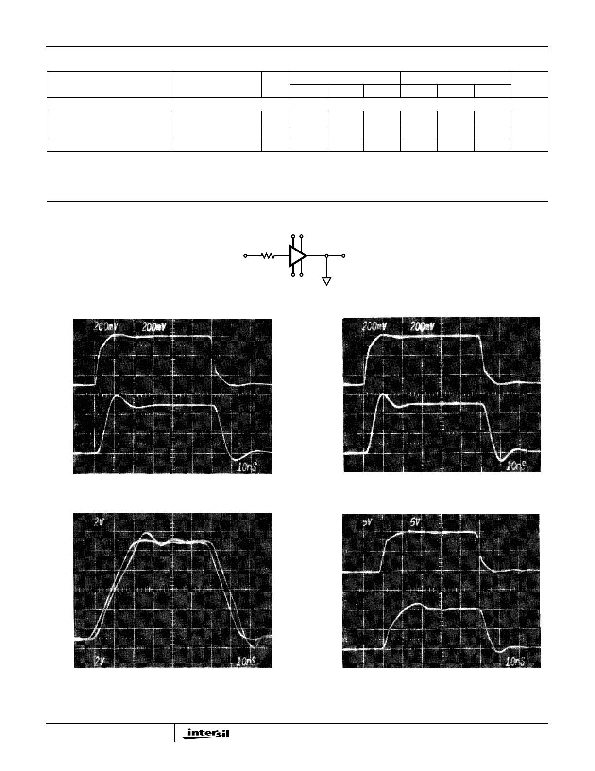
Test Circuit and Waveforms
+15V
-15V
+
V
2
OUTIN
V
-V1-
2
R
L
V1+
R
S
FIGURE 1. LARGE AND SMALL SIGNAL RESPONSE
V
V
V
OUT
V
OUT
V
V
OUT
IN
RS = 50Ω, RL = 1kΩ
IN
RS = 50Ω, RL = 100Ω
SMALL SIGNAL WAVEFORMS SMALL SIGNAL WAVEFORMS
IN
V
V
OUT
IN
RS = 50Ω, RL = 100Ω
RS = 50Ω, RL = 1kΩ
LARGE SIGNAL WAVEFORMS LARGE SIGNAL WAVEFORMS
3
Page 4
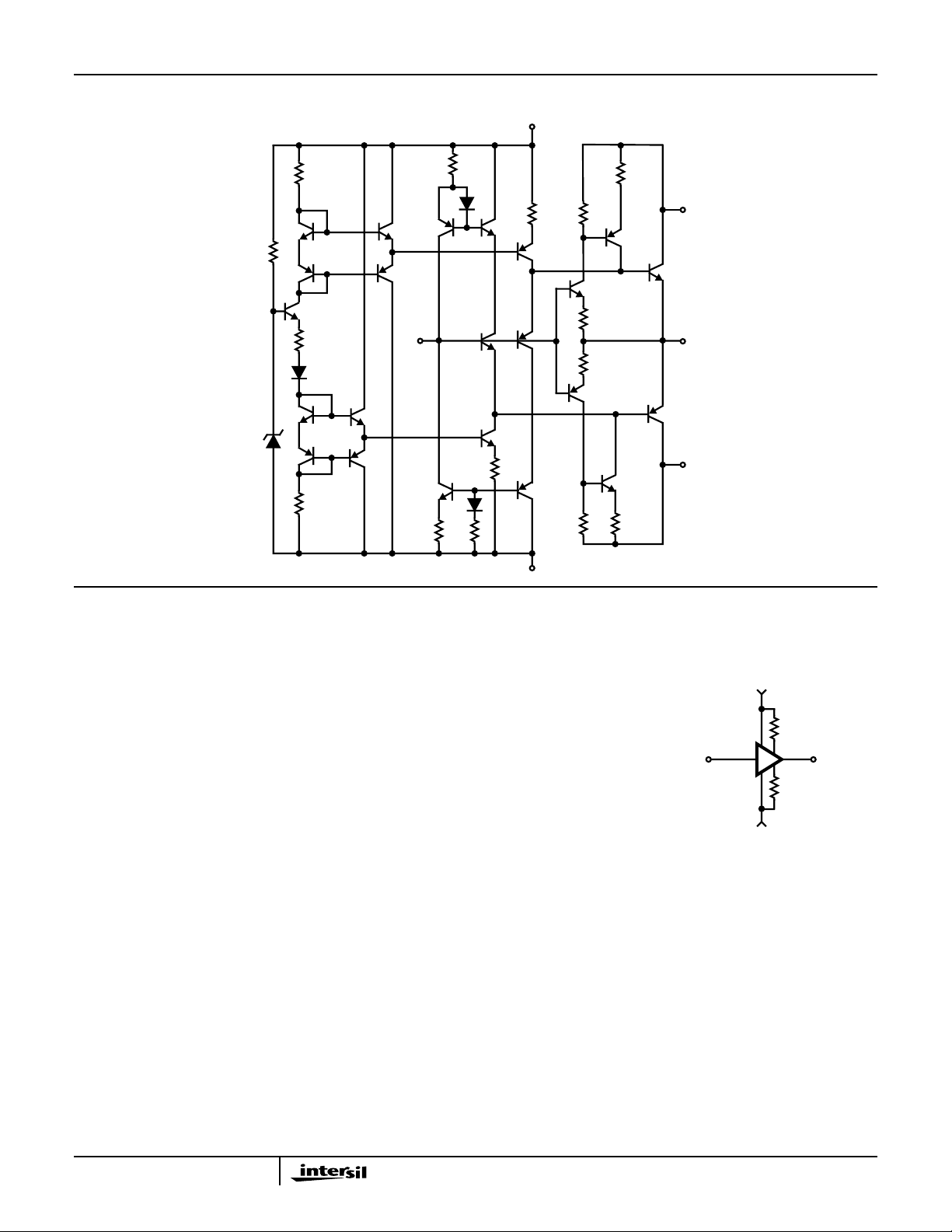
Schematic Diagram
HA-5002
V
+
1
R
R
9
Q
25
R
10
Q
9
Q
10
R
5
Q
21
Q
11
Q
15
Q
23
R
7
Q
22
Q
24
8
Q
19
R
Q
20
Q
26
Q
27
IN
Q
16
R
12
Q
Q7Q
Q
8
R
Q
17
R
3
4
18
Q
3
4
6
Q
14
R
2
R
N1
R
1
Q
12
Q
6
R
11
R
N2
Q
5
Q
13
R
N3
V2+
Q
1
OUT
Q
2
V2-
Application Information
Layout Considerations
The wide bandwidth of the HA-5002 necessitates that high
frequency circuit layout procedures be followed. Failure to
follow these guidelines can result in marginal performance.
Probably the most crucial of the RF/video layout rules is the
use of a ground plane. A ground plane provides isolation and
minimizes distributed circuit capacitance and inductance
which will degrade high frequency performance.
Other considerations are proper power supply bypassing
and keeping the input and output connections as short as
possible which minimizes distributed capacitance and
reduces board space.
Power Supply Decoupling
For optimal device performance, it is recommended that the
positive and negative power supplies be bypassed with
capacitors to ground. Ceramic capacitors ranging in value
from 0.01 to 0.1µF will minimize high frequency variations in
supply voltage, while low frequency bypassing requires
larger valued capacitors since the impedance of the
capacitor is dependent on frequency.
It is also recommended that the bypass capacitors be
connected close to the HA-5002 (preferably directly to the
supply pins).
Operation at Reduced Supply Levels
The HA-5002 can operate at supply voltage levels as low as
±5V and lower. Output swing is directly affected as well as
slight reductions in slew rate and bandwidth.
V1-
Short Circuit Protection
The output current can be limited by using the following circuit:
I
R
LIM
V+
------------------------- -
I
OUTMAX
V-
------------------------- -==
I
OUTMAX
V+
V
+
1
IN
V1-
V-
= 200mA
OUTMAX
(CONTINUOUS)
R
LIM
V2+
OUT
V
-
2
R
LIM
Capacitive Loading
The HA-5002 will drive large capacitive loads without oscillation
but peak current limits should not be exceeded. F ollo wing the
formula I = Cdv/dt implies that the slew rate or the capacitive
load must be controlled to keep peak current below the
maximum or use the current limiting approach as shown. The
HA-5002 can become unstable with small capacitive loads
(50pF) if certain precautions are not taken. Stability is
enhanced by any one of the follo wing: a source resistance in
series with the input of 50Ω to 1kΩ; increasing capacitive load
to 150pF or greater; decreasing C
an output resistor of 10Ω to 50Ω; or adding feedback
capacitance of 50pF or greater. Adding source resistance
generally yields the best results.
to 20pF or less; adding
LOAD
4
Page 5

1.8
1.6
1.4
CAN
1.2
1.0
0.8
SOIC
0.6
0.4
MAXIMUM POWER DISSIPATION (W)
0.2
0.0
25
QUIESCENT POWER DISSIPATION
AT ±15V SUPPLIES
45
Typical Application
HA-5002
PLCC
CERDIP
PDIP
65 85
TEMPERATURE (
o
105
C)
125
FIGURE 2. MAXIMUM POWER DISSIPATION vs TEMPERATURE
P
DMAX
Where: T
JMAX
Device
TA = Ambient
θJC = Junction to Case Thermal Resistance
= Case to Heat Sink Thermal Resistance
θ
CS
θ
= Heat Sink to Ambient Thermal Resistance
SA
Graph is based on:
T
–
JMAXTA
--------------------------------------------=
++
θ
JCθCSθSA
= Maximum Junction T emper ature of the
T
–
JMAXTA
P
DMAX
--------------------------------=
θ
JA
+12V
V1+V2+
R
S
V
50Ω
IN
V1-V2-
-12V
R
50Ω
M
Typical Performance Curves
9
VS = ±15V, RS = 50Ω
6
3
0
-3
-6
-9
VOLTAGE GAIN (dB)
-12
-15
-18
1 10 100
GAIN
PHASE
FREQUENCY (MHz)
V
V
IN
OUT
RG -58
V
OUT
RL 50Ω
FIGURE 3. COAXIAL CABLE DRIVER - 50Ω SYSTEM
9
VS = ±15V, RS = 50Ω
6
3
0
-3
0
45
90
135
180
o
o
o
o
o
PHASE SHIFT
-6
-9
VOLTAGE GAIN (dB)
-12
-15
-18
1 10 100
GAIN
PHASE
FREQUENCY (MHz)
o
0
45
90
135
180
o
o
o
o
PHASE SHIFT
FIGURE 4. GAIN/PHASE vs FREQUENCY (RL = 1kΩ) FIGURE 5. GAIN/PHASE vs FREQUENCY (RL = 50Ω)
5
Page 6

Typical Performance Curves (Continued)
HA-5002
0.994
0.992
0.990
0.988
0.986
0.984
0.982
0.980
VOLTAGE GAIN (V/V)
0.978
0.976
0.974
VS = ±15V
V
= -10V TO +10V
OUT
0 20 40 60 80 100 120-20-40-60
TEMPERATURE (oC)
0.998
0.997
0.996
0.995
0.994
0.993
VOLTAGE GAIN (V/V)
0.992
0.991
VS = ±15V
V
OUT
V
= 0 TO -10V
OUT
0 20 40 60 80 100 120-20-40-60
TEMPERATURE (oC)
= 0 TO +10V
FIGURE 6. VOLTAGE GAIN vs TEMPERATURE (RL = 100Ω) FIGURE 7. VOLTAGE GAIN vs TEMPERATURE (RL = 1kΩ)
3
2
1
0
-1
-2
-3
-4
-5
-6
-7
OFFSET VOLTAGE (mV)
-8
-9
-10
-11
VS = ±15V
0 20 40 60 80 100 120-20-40-60
TEMPERATURE (oC)
7
VS = ±15V
6
5
4
3
2
BIAS CURRENT (µA)
1
0
0 20 40 60 80 100 120-20-40-60
TEMPERATURE (oC)
FIGURE 8. OFFSET VOLTAGE vs TEMPERATURE FIGURE 9. BIAS CURRENT vs TEMPERATURE
15
14
13
OUTPUT VOLTAGE (V)
12
11
VS = ±15V, R
= 100Ω
LOAD
+V
OUT
-V
OUT
0 20 40 60 80 100 120-20-40-60
TEMPERATURE (oC)
10
VS = ±15V, I
9
8
7
6
5
SUPPLY CURRENT (mA)
4
3
= 0mA
OUT
0 20 40 60 80 100 120-20-40-60
TEMPERATURE (oC)
FIGURE 10. MAXIMUM OUTPUT VOLTAGE vs TEMPERATURE FIGURE 11. SUPPLY CURRENT vs TEMPERATURE
6
Page 7

Typical Performance Curves (Continued)
HA-5002
10
I
= 0mA
OUT
8
6
4
SUPPLY CURRENT (mA)
2
0
024681012141618
125oC, 25oC
-55oC
SUPPLY VOLTAGE (±V)
IMPEDANCE (Ω)
VS = ±15V
100K
Z
10K
1000
100
10
1
100K 1M 10M 100M
IN
Z
OUT
FREQUENCY (Hz)
FIGURE 12. SUPPLY CURRENT vs SUPPLY VOLTAGE FIGURE 13. INPUT/OUTPUT IMPEDANCE vs FREQUENCY
23
22
21
20
19
18
17
AT 100kHz
16
P-P
15
14
13
MAX, V
12
11
OUT
V
10
9
8
7
15 12 8 5
T
= 125oC,
A
TA = -55oC
SUPPLY VOLTAGE (±V)
TA = 25oC
R
LOAD
= 100Ω
80
70
60
50
40
PSRR (dB)
30
20
10
0
10K 100K 1M 10M
FREQUENCY (Hz)
100M
FIGURE 14. V
1500
1400
1300
1200
1100
SLEW RATE (V/µs)
1000
900
6 8 10 12 14 16 18
MAXIMUM vs V
OUT
SUPPLY VOLTAGE (±V)
SUPPLY
FIGURE 15. PSRR vs FREQUENCY
150
100
50
(mV)
RL = 1K
IN
0
- V
OUT
V
-50
-100
-150
-10 -8 -6 -4 -2
RL = 100
0246810
INPUT VOLTAGE (VOLTS)
FIGURE 16. SLEW RATE vs SUPPLY VOLTAGE FIGURE 17. GAIN ERROR vs INPUT VOLTAGE
7
V
= ±15V
S
TA = 25oC
RL = 600
Page 8

Die Characteristics
DIE DIMENSIONS:
HA-5002
SUBSTRATE POTENTIAL (Powered Up):
81 mils x 80 mils x 19 mils
2050µm x 2030µm x 483µm
METALLIZATION:
Type: Al, 1% Cu
Thickness: 20k
Å ±2kÅ
PASSIVATION:
Type: Nitride (Si3N4) over Silox (SiO2, 5% Phos.)
Silox Thickness: 12k
Å ±2kÅ
Nitride Thickness: 3.5kÅ ±1.5kÅ
Metallization Mask Layout
V
+ (ALT)
1
V1-
V1-
TRANSISTOR COUNT:
27
PROCESS:
Bipolar Dielectric Isolation
HA-5002
IN
V1- (ALT)
V
+
2
OUT
-
V
2
+
V
1
8
Page 9

Metal Can Packages (Can)
REFERENCE PLANE
A
ØD ØD1
F
Q
Øb1
L
L2
L1
A
A
Øe
Øb1
Øb
BASE AND
SEATING PLANE
BASE METAL LEAD FINISH
SECTION A-A
NOTES:
1. (All leads) Øb applies between L1 and L2. Øb1 applies between
L2 and 0.500 from the reference plane. Diameter is uncontrolled
in L1 and beyond 0.500 from the reference plane.
2. Measured from maximum diameter of the product.
3. α is the basic spacing from the centerline of the tab to terminal 1
and β is the basic spacing of each lead or lead position (N -1
places) from α, looking at the bottom of the package.
4. N is the maximum number of terminal positions.
5. Dimensioning and tolerancing per ANSI Y14.5M - 1982.
6. Controlling dimension: INCH.
Øb2
e1
ØD2
2
β
N
1
α
k
HA-5002
k1
C
L
T8.C MIL-STD-1835 MACY1-X8 (A1)
8 LEAD METAL CAN PACKAGE
INCHES MILLIMETERS
SYMBOL
A 0.165 0.185 4.19 4.70 -
Øb 0.016 0.019 0.41 0.48 1
Øb1 0.016 0.021 0.41 0.53 1
Øb2 0.016 0.024 0.41 0.61 -
ØD 0.335 0.375 8.51 9.40 ØD1 0.305 0.335 7.75 8.51 ØD2 0.110 0.160 2.79 4.06 -
e 0.200 BSC 5.08 BSC -
e1 0.100 BSC 2.54 BSC -
F - 0.040 - 1.02 -
k 0.027 0.034 0.69 0.86 -
k1 0.027 0.045 0.69 1.14 2
L 0.500 0.750 12.70 19.05 1
L1 - 0.050 - 1.27 1
L2 0.250 - 6.35 - 1
Q 0.010 0.045 0.25 1.14 -
α
45o BSC 45o BSC 3
β 45o BSC 45o BSC 3
N8 84
NOTESMIN MAX MIN MAX
Rev. 0 5/18/94
9
Page 10

Dual-In-Line Plastic Packages (PDIP)
HA-5002
N
D1
E1
-B-
-C-
E
A2
A
L
A
1
e
C
C
L
e
A
C
e
B
INDEX
AREA
BASE
PLANE
SEATING
PLANE
D1
B1
1 2 3 N/2
-AD
e
B
0.010 (0.25) C AM BS
NOTES:
7. Controlling Dimensions: INCH. In case of conflict between
English and Metric dimensions, the inch dimensions control.
8. Dimensioning and tolerancing per ANSI Y14.5M-1982.
9. Symbols are defined in the “MO Series Symbol List” in Section
2.2 of Publication No. 95.
10. Dimensions A, A1 and L are measured with the package seated
in JEDEC seating plane gauge GS-3.
11. D, D1, and E1 dimensions do not include mold flash or protrusions. Mold flash or protrusions shall not exceed 0.010 inch
(0.25mm).
12. E and are measured with the leads constrained to be per-
e
pendicular to datum .
A
-C-
13. eB and eC are measured at the lead tips with the leads unconstrained. eC must be zero or greater.
14. B1 maximum dimensions do not include dambar protrusions.
Dambar protrusions shall not exceed 0.010 inch (0.25mm).
15. N is the maximum number of terminal positions.
16. Corner leads (1, N, N/2 and N/2 + 1) for E8.3, E16.3, E18.3,
E28.3, E42.6 will have a B1 dimension of 0.030 - 0.045 inch
(0.76 - 1.14mm).
E8.3 (JEDEC MS-001-BA ISSUE D)
8 LEAD DUAL-IN-LINE PLASTIC PACKAGE
INCHES MILLIMETERS
SYMBOL
A - 0.210 - 5.33 4
A1 0.015 - 0.39 - 4
A2 0.115 0.195 2.93 4.95 -
B 0.014 0.022 0.356 0.558 B1 0.045 0.070 1.15 1.77 8, 10
C 0.008 0.014 0.204 0.355 -
D 0.355 0.400 9.01 10.16 5
D1 0.005 - 0.13 - 5
E 0.300 0.325 7.62 8.25 6
E1 0.240 0.280 6.10 7.11 5
e 0.100 BSC 2.54 BSC -
e
A
e
B
0.300 BSC 7.62 BSC 6
- 0.430 - 10.92 7
L 0.115 0.150 2.93 3.81 4
N8 89
NOTESMIN MAX MIN MAX
Rev. 0 12/93
10
Page 11

HA-5002
Plastic Leaded Chip Carrier Packages (PLCC)
0.042 (1.07)
0.048 (1.22)
PIN (1) IDENTIFIER
0.020 (0.51) MAX
3 PLCS
C
L
D1
D
0.026 (0.66)
0.032 (0.81)
0.045 (1.14)
MIN
0.042 (1.07)
0.056 (1.42)
0.050 (1.27) TP
VIEW “A” TYP.
C
L
EE1
0.013 (0.33)
0.021 (0.53)
0.025 (0.64)
MIN
0.004 (0.10) C
0.025 (0.64)
0.045 (1.14)
D2/E2
D2/E2
A1
A
-C-
VIEW “A”
0.020 (0.51)
MIN
SEATING
PLANE
N20.35 (JEDEC MS-018AA ISSUE A)
20 LEAD PLASTIC LEADED CHIP CARRIER PACKAGE
R
SYMBOL
A 0.165 0.180 4.20 4.57 -
A1 0.090 0.120 2.29 3.04 -
D 0.385 0.395 9.78 10.03 D1 0.350 0.356 8.89 9.04 3
D2 0.141 0.169 3.59 4.29 4, 5
E 0.385 0.395 9.78 10.03 E1 0.350 0.356 8.89 9.04 3
E2 0.141 0.169 3.59 4.29 4, 5
N20 206
INCHES MILLIMETERS
NOTESMIN MAX MIN MAX
Rev. 2 11/97
NOTES:
17. Controlling dimension: INCH. Converted millimeter dimensions
are not necessarily exact.
18. Dimensions and tolerancing per ANSI Y14.5M-1982.
19. Dimensions D1 and E1 donot include mold protrusions. Allowable
mold protrusion is 0.010 inch (0.25mm) per side. Dimensions D1
and E1 include mold mismatch and are measured at the extreme
material condition at the body parting line.
20. To be measured at seating plane contact point.
-C-
21. Centerline to be determined where center leads exit plastic body.
22. “N” is the number of terminal positions.
11
Page 12

HA-5002
Ceramic Dual-In-Line Frit Seal Packages (CERDIP)
c1
LEAD FINISH
-A-
-B-
bbb C A - B
S
BASE
PLANE
SEATING
PLANE
S1
b2
b
ccc C A - BMD
D
A
A
e
S
S
NOTES:
23. Index area: A notch or a pin one identification mark shall be located adjacent to pin one and shall be located within the shaded
area shown. The manufacturer’s identification shall not be used
as a pin one identification mark.
24. The maximum limits of lead dimensions b and c or M shall be
measured at the centroid of the finished lead surfaces, when
solder dip or tin plate lead finish is applied.
25. Dimensions b1 and c1 apply to lead base metal only. Dimension
M applies to lead plating and finish thickness.
26. Corner leads (1, N, N/2, and N/2+1) may be configured with a
partial lead paddle. For this configuration dimension b3 replaces
dimension b2.
27. This dimension allows for off-center lid, meniscus, and glass
overrun.
28. Dimension Q shall be measured from the seating plane to the
base plane.
29. Measure dimension S1 at all four corners.
30. N is the maximum number of terminal positions.
31. Dimensioning and tolerancing per ANSI Y14.5M - 1982.
32. Controlling dimension: INCH
-DBASE
E
D
S
S
Q
A
-CL
METAL
b1
M
(b)
SECTION A-A
α
(c)
M
eA
eA/2
aaa C A - B
M
c
D
S
S
F8.3A MIL-STD-1835 GDIP1-T8 (D-4, CONFIGURATION A)
8 LEAD CERAMIC DUAL-IN-LINE FRIT SEAL PACKAGE
INCHES MILLIMETERS
SYMBOL
A - 0.200 - 5.08 -
b 0.014 0.026 0.36 0.66 2
b1 0.014 0.023 0.36 0.58 3
b2 0.045 0.065 1.14 1.65 b3 0.023 0.045 0.58 1.14 4
c 0.008 0.018 0.20 0.46 2
c1 0.008 0.015 0.20 0.38 3
D - 0.405 - 10.29 5
E 0.220 0.310 5.59 7.87 5
e 0.100 BSC 2.54 BSC eA 0.300 BSC 7.62 BSC -
eA/2 0.150 BSC 3.81 BSC -
L 0.125 0.200 3.18 5.08 -
Q 0.015 0.060 0.38 1.52 6
S1 0.005 - 0.13 - 7
o
α
90
105
o
90
o
105
aaa - 0.015 - 0.38 bbb - 0.030 - 0.76 -
ccc - 0.010 - 0.25 -
M - 0.0015 - 0.038 2, 3
N8 88
NOTESMIN MAX MIN MAX
o
Rev. 0 4/94
-
12
Page 13

Small Outline Plastic Packages (SOIC)
HA-5002
N
INDEX
AREA
123
-A-
E
-B-
SEATING PLANE
D
A
-C-
0.25(0.010) BM M
H
L
h x 45
o
α
e
B
0.25(0.010) C AM BS
M
NOTES:
33. Symbols are defined in the “MO Series Symbol List” in Section 2.2 of
Publication Number 95.
34. Dimensioning and tolerancing per ANSI Y14.5M-1982.
35. Dimension “D” does not include mold flash, protrusions or gateburrs.
Mold flash, protrusion and gate burrsshall not exceed 0.15mm (0.006
inch) per side.
36. Dimension “E” does not include interlead flash or protrusions. Interlead flash and protrusions shall not exceed 0.25mm (0.010 inch) per
side.
37. The chamfer on the body is optional. If it is not present, a visual index
feature must be located within the crosshatched area.
38. “L” is the length of terminal for soldering to a substrate.
39. “N” is the number of terminal positions.
40. Terminal numbers are shown for reference only.
41. The lead width “B”, as measured 0.36mm (0.014 inch) or greater
above the seating plane, shall not exceed a maximum value of
0.61mm (0.024 inch).
42. Controlling dimension: MILLIMETER. Converted inch dimensions
are not necessarily exact.
A1
C
0.10(0.004)
M8.15 (JEDEC MS-012-AA ISSUE C)
8 LEAD NARROW BODY SMALL OUTLINE PLASTIC
PACKAGE
INCHES MILLIMETERS
SYMBOL
A 0.0532 0.0688 1.35 1.75 -
A1 0.0040 0.0098 0.10 0.25 -
B 0.013 0.020 0.33 0.51 9
C 0.0075 0.0098 0.19 0.25 D 0.1890 0.1968 4.80 5.00 3
E 0.1497 0.1574 3.80 4.00 4
e 0.050 BSC 1.27 BSC -
H 0.2284 0.2440 5.80 6.20 -
h 0.0099 0.0196 0.25 0.50 5
L 0.016 0.050 0.40 1.27 6
N8 87
o
α
0
o
8
o
0
o
8
Rev. 0 12/93
NOTESMIN MAX MIN MAX
-
All Intersil semiconductor products are manufactured, assembled and tested under ISO9000 quality systems certification.
Intersil semiconductor products are sold by description only.Intersil Corporation reserves the right to make changes in circuit design and/or specifications at any time without notice. Accordingly, the reader is cautioned to verify that data sheets are current before placing orders. Information furnished by Intersil is believed to be accurate and
reliable. However ,no responsibility is assumed by Intersil or its subsidiaries for its use; nor for any infringements of patents or other rights of third parties which may result
from its use. No license is granted by implication or otherwise under any patent or patent rights of Intersil or its subsidiaries.
For information regarding Intersil Corporation and its products, see web site www.intersil.com
Sales Office Headquarters
NORTH AMERICA
Intersil Corporation
P. O. Box 883, Mail Stop 53-204
Melbourne, FL 32902
TEL: (321) 724-7000
FAX: (321) 724-7240
13
EUROPE
Intersil SA
Mercure Center
100, Rue de la Fusee
1130 Brussels, Belgium
TEL: (32) 2.724.2111
FAX: (32) 2.724.22.05
ASIA
Intersil (Taiwan) Ltd.
7F-6, No. 101 Fu Hsing North Road
Taipei, Taiwan
Republic of China
TEL: (886) 2 2716 9310
FAX: (886) 2 2715 3029
 Loading...