

Page 1

HA13143
Four-Channel BTL Driver for CD Players
ADE-207-330 (Z)
1st Edition
Dec. 2000
Description
HA13143 is a four-channel BTL driver IC for driving CD player actuators (focus and tracking) and motors
(carriage and spindle). It is ideal for small-profile players, since it requires few external parts and adopts a
compact, surface-mounting package (MP-26 DT).
Functions
• 4-channel BTL driver
• 5 V power-supply circuit
• Standby circuit
• Built-in protection circuits (surge current, TSD)
Features
• Four channels for driving the actuators and motors in a CD player
• High driving current
• Built-in protection against surge currents from other circuits or from short circuits
• Built-in thermal shutdown protection circuit with hysteresis
• Built-in 5 V power supply (uses external pnp transistor)
• Compact MP-26 DT surface-mounting package enabling use in small-profile players
Page 2
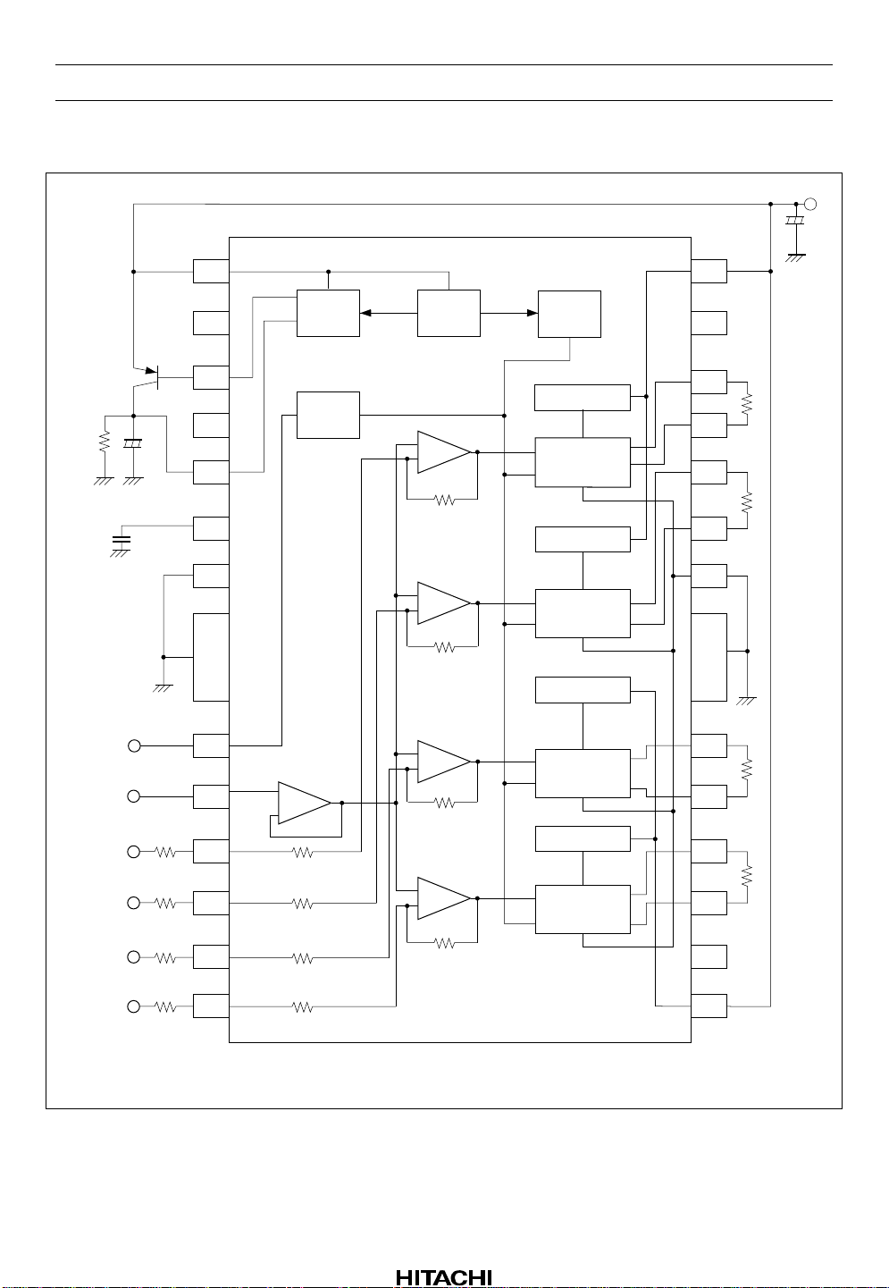
HA13143
Block Diagram
Q1
+
R5
16/2 W
C2
100
µF
C3
1000 pF
BYPASS
V
CC
1
NC
2
CD5B
3
NC
4
CD5V
5
6
AGND
7
5 V
fixed
voltage
CONT
circuit
+
–
+
–
BAND
GAP
28.2 k
TSD
Limiter circuit
BTL driver
Limiter circuit
BTL driver
PV
CC
26
Vop2
25
CO+
24
CO–
23
SO+
22
SO–
21
PGND
20
V
CC
+
C1
470
2
8
7
µF
Input
5.0 V
2.5 V
TAB TAB
CONT
8
R1
1 k
R2
1 k
R3
1 k
R4
1 k
VREF
9
CIN
10
SIN
11
FIN
12
TIN
13
+
–
9 k
9 k
9 k
9 k
+
–
+
–
28.2 k
Limiter circuit
BTL driver
28.2 k
Limiter circuit
BTL driver
28.2 k
Unit:
Fo+
19
Fo–
18
To+
17
To–
16
Vop1
15
PV
14
R: Ω
C: F
12.5
12.5
1
CC
Rev.1, Dec. 2000, page 2 of 7
Page 3
HA13143
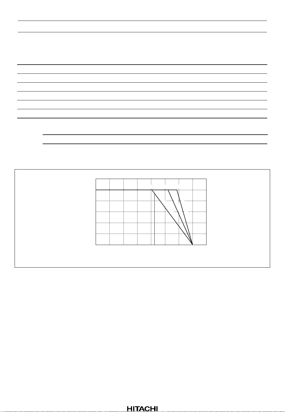
Absolute Maximum Ratings (Ta = 25°C)
Item Symbol Rating Unit Remarks
Supply voltage V
CC
Output current IO-Peak See Note 1 A 1
Power dissipation P
T
Operating temperature Topr –30 to +85 °C
Storage temperature Tstg –55 to +125 °C
Junction temperature Tj 150 °C
Notes: 1. Output current from each channel is as shown in table below.
Focus Tracking Carriage Spindle Unit
Max. output current 1200 1200 1200 1400 mA
2. In normal play mode.
3. Usable operating voltage range Vopr = 7 to 10 V.
4. The derating curve is as shown in the graph below (θjc = 8.0°C max.).
18 V
2.5 W 2
3.0
2.5
T
2.0
1.5
1.0
0.5
Power dissipation P (W)
0
0 25 50 75 85 100 125 150 175
–30
Ambient temperature T
θf = thermal resistance of heat sink
80˚C 105˚C 120˚C
θ
f = 20˚C/W
Infinite heat sink
θ
f
= 10˚C/W
(˚C)
a
Rev.1, Dec. 2000, page 3 of 7
Page 4

HA13143
Electrical Characteristics (Ta = 25°C, VCC = 8.0 V)
Applicable
Item Symbol Min Typ Max Unit Test Conditions
Output voltage with stable 5
V power supply
Ripple rejection SVR vs 40 — — dB 5
Output leakage current Io L5B — — 1.0 µA VCC = 0 V 3
Focus driver
Output voltage Vfo 3.75 3.95 4.15 V RL = 12.5 Ω 19, 20
Output offset voltage VooF fo –110 0 +110 mV RL = 12.5 Ω 19, 20
Gain Gv fo 14 15 16 dB RL = 12.5 Ω,
Max. output amplitude Vo fo 5.2 — — V RL = 12.5 Ω 19, 20
Ripple rejection SVR fo 30 — — dB 19, 20
Cutoff frequency Fc fo 50 100 200 kHz 19, 20
Tracking driver
Output voltage Vtr 3.75 3.95 4.15 V RL = 12.5 Ω 16, 17
Output offset voltage VooFtr –110 0 +110 mV RL = 12.5 Ω 16, 17
Gain Gv tr 14 15 16 dB RL = 12.5 Ω,
Max. output amplitude Vo tr 5.2 — — V RL = 12.5 Ω 16, 17
Ripple rejection SVRtr 30 — — dB 16, 17
Cutoff frequency fctr 50 100 200 kHz 16, 17
Spindle driver
Output voltage Vsp 3.80 4.00 4.20 V RL = 7.0 Ω 21, 22
Output offset voltage VooFsp –110 0 +110 mV RL = 7.0 Ω 21, 22
Gain Gvsp 14 15 16 dB RL = 7.0 Ω,
Max. output amplitude Vo sp 4.2 — — V RL = 7.0 Ω 21, 22
Ripple rejection SVR sp 30 — — dB 21, 22
Cutoff frequency fcsp 50 100 200 kHz 21, 22
Carriage driver
Output voltage Vcr 3.80 4.00 4.20 V RL = 8.0 Ω 23, 24
Output offset voltage VooF cr –110 0 +110 mV RL = 8.0 Ω 23, 24
Gain Gvcr 14 15 16 dB RL = 8.0 Ω,
Max. output amplitude Vocr 4.2 — — V RL = 8.0 Ω 23, 24
Ripple rejection SVR cr 30 — — dB 23, 24
Cutoff frequency Fccr 50 100 200 kHz 23, 24
Vs 4.65 5.00 5.35 V IL = 300 mA 5
fin = 1 kHz
fin = 1 kHz
fin = 1 kHz
fin = 1 kHz
Pins
19, 20
16, 17
21, 22
23, 24
Rev.1, Dec. 2000, page 4 of 7
Page 5

HA13143
Electrical Characteristics (Ta = 25°C, VCC = 8.0 V) (cont)
Applicable
Item Symbol Min Typ Max Unit Test Conditions
Channel crosstalk CT 50 — — dB fin = 1 kHz, 4 ch 16, 17, 18,
Operating voltage (1) Vop1 3.75 3.95 4.15 V Actuators 16
Operating voltage (2) Vop2 3.80 4.00 4.20 V Motors 25
Protection circuits
Limiter operating current
I
fo — 860 — mA 18, 19
LMT
Focus
Limiter operating current
I
tr — 860 — mA 16, 17
LMT
Tracking
Limiter operating current
I
sp — 1100 — mA 21, 22
LMT
Spindle
Limiter operating current
I
cr — 930 — mA 23, 24
LMT
Carriage
TSD operating temperature Ttsd — 165 — °C
TSD hysteresis temperature Thys — 30 — °C
CONT circuit High-level
VIHcut — — 3.0 V 8
input voltage
0Low-level input voltage VILcut 2.0 — — V 8
High-level input current IIHcut 0.3 1.0 5.0 µA CONT = 3.0 V 8
Low-level input current IILcut — — 0.1 µA CONT = 2.0 V 8
Circuit current when no
signal (standby)
Circuit current when no
signal (standby)
Circuit current when no
signal
Istby 1 4.0 6.0 10.0 mA CONT = 2.0 V
BYPASS = OPEN
Istby 2 3.0 5.0 9.0 mA CONT = 3.0 V
BYPASS = “L”
Icc 1 102030mACONT = 3.0 V
BYPASS = OPEN
Bypass voltage Vbps 1.3 1.45 1.6 V 6
Driving performance Focus Io fo 500 860 — mA 18, 19
Driving performance
Io tr 500 860 — mA 16, 17
Tracking
Driving performance Spindle Io sp 750 1100 — mA 21, 22
Driving performance
Io cr 650 930 — mA 23, 24
Carriage
Pins
19, 21, 22,
23, 24
1, 14, 26
1, 14, 26
1, 14, 26
Rev.1, Dec. 2000, page 5 of 7
Page 6

HA13143
Package Dimensions
26
18.4
19.2 Max
14
8.30
+ 0.37
– 0.23
9.83
Unit: mm
1
0.80
0.35 ± 0.08
2.8
1.20 Max
3.6
6.4
0.16
13
3.00 Max
+ 0.10
0.3
– 0.05
+ 0.15
– 0.10
9.53
0.10
M
0.10
Hitachi Code
JEDEC
EIAJ
Mass
(reference value)
MP-26DT
—
—
0.98 g
Rev.1, Dec. 2000, page 6 of 7
Page 7

HA13143
Disclaimer
1. Hitachi neither warrants nor grants licenses of any rights of Hitachi’s or any third party’s patent,
copyright, trademark, or other intellectual property rights for information contained in this document.
Hitachi bears no responsibility for problems that may arise with third party’s rights, in cluding
intellectual property rights, in connection with u se of the information contained in this document.
2. Products and product specifications may be subject to change without notice. Confirm that you have
received the latest product standards or specifications before final design, purchase or use.
3. Hitachi makes every attempt to ensure that its products ar e of h igh quality and reliability. However,
contact Hitachi’s sales office before using the product in an application that demands especially high
quality and reliability or where its failure or malfunction may directly threaten human life or cause risk
of bodily injury, such as aerospace, aeronautics, nuclear power, combustion control, transportation,
traffic, safety equipment or medical equipment for life support.
4. Design your application so that the product is used within the ranges guaranteed by Hitachi particularly
for maximum rating, operating supply voltage range, heat radiation characteristics, installation
conditions and other characteristics. Hitachi bears no responsibility for failure or damage when used
beyond the guaranteed ranges. Even within the guaranteed ranges, consider normally foreseeable
failure rates or failure modes in semiconductor devices and employ systemic measures such as failsafes, so that the equipment incorporating Hitachi product does not cause bodily injury, fire or other
consequential damage due to operation of the Hitachi product.
5. This product is not designed to be radiation resistant.
6. No one is permitted to reproduce or duplicate, in any form, the whole or part of this document without
written approval from Hitachi.
7. Contact Hitachi’s sales office for any questions regarding this document or Hitachi semiconductor
products.
Sales Offices
Hitachi, Ltd.
Semiconductor & Integrated Circuits.
Nippon Bldg., 2-6-2, Ohte-machi, Chiyoda-ku, Tokyo 100-0004, Japan
Tel: Tokyo (03) 3270-2111 Fax: (03) 3270-5109
URL NorthAmerica : http://semiconductor.hitachi.com/
For further information write to:
Hitachi Semiconductor
(America) Inc.
179 East Tasman Drive,
San Jose,CA 95134
Tel: <1> (408) 433-1990
Fax: <1>(408) 433-0223
Europe : http://www.hitachi-eu.com/hel/ecg
Asia : http://sicapac.hitachi-asia.com
Japan : http://www.hitachi.co.jp/Sicd/indx.htm
Hitachi Europe GmbH
Electronic Components Group
Dornacher Straße 3
D-85622 Feldkirchen, Munich
Germany
Tel: <49> (89) 9 9180-0
Fax: <49> (89) 9 29 30 00
Hitachi Europe Ltd.
Electronic Components Group.
Whitebrook Park
Lower Cookham Road
Maidenhead
Berkshire SL6 8YA, United Kingdom
Tel: <44> (1628) 585000
Fax: <44> (1628) 585160
Hitachi Asia Ltd.
Hitachi Tower
16 Collyer Quay #20-00,
Singapore 049318
Tel : <65>-538-6533/538-8577
Fax : <65>-538-6933/538-3877
URL : http://www.hitachi.com.sg
Hitachi Asia Ltd.
(Taipei Branch Office)
4/F, No. 167, Tun Hwa North Road,
Hung-Kuo Building,
Taipei (105), Taiwan
Tel : <886>-(2)-2718-3666
Fax : <886>-(2)-2718-8180
Telex : 23222 HAS-TP
URL : http://www.hitachi.com.tw
Hitachi Asia (Hong Kong) Ltd.
Group III (Electronic Components)
7/F., North Tower,
World Finance Centre,
Harbour City, Canton Road
Tsim Sha Tsui, Kowloon,
Hong Kong
Tel : <852>-(2)-735-9218
Fax : <852>-(2)-730-0281
URL : http://www.hitachi.com.hk
Copyright Hitachi, Ltd., 2000. All rights reserved. Printed in Japan.
Colophon 2.0
Rev.1, Dec. 2000, page 7 of 7
 Loading...