

Page 1

HA12188AF
Pre-Amplifier and Servo IC for Quadruple-Speed CD-ROM
ADE-207-183(Z)
1st. Edition
October 1995
Description
The typical values of built-in capacitances in this IC are reduced 10% compared with those in I C
HA12188F. The values of Electrical Characteristics of this IC are same as those of IC HA12188F.
Functions
• RF amplifier
• Focus error amplifier
• Tracking error amplifier
• FOK detector
• Mirror detector
• Defect detector
• APC amplifier
• Focus, tracking, and sled servo control
• Inner/outer direction detector
Features
• Built-in variable resistors for adjusting tracking error EF balance, tracking gain, and focus g ain
• Single power supply
• Supports double and quadruple speeds
• Few external components
• FP-56 package
Page 2
HA12188AF
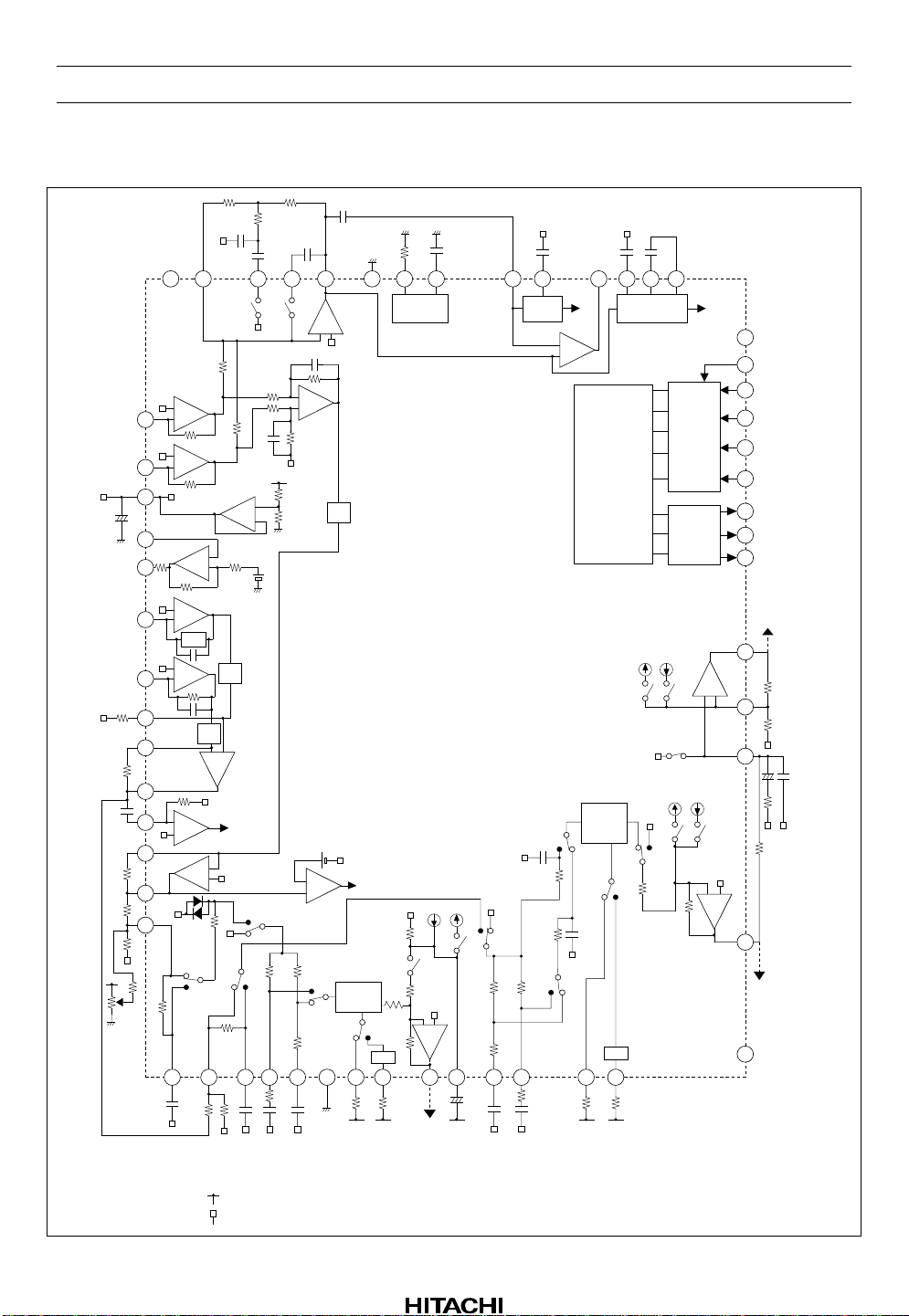
Block Diagram
V
CC
40
RFS
RS2
RF1
+
–
43
RF2
+
–
44
45
+
APC
46
47
48
TR2
49
+
–
+
–
BAL
TR1
+
–
VR
RS1
–+
–
+
FE
+
–
VR
50
51
VR
–+
TE
52
+
53
–
FA
TZC
–
+
FS4
FZC
–
+
54
55
56
DS1
FLS
Phase
compen.
×2.7
FPS
Focus
bias
adj.
DS2
1 2 5 6
3 4 7 8 9
• The states of the IC’s internal switches at XRST = “L” are shown at block diagram.
• The black dot symbol of transfer switch shows on state.
• The symbols “ ” mean connecting to V
• The symbols “ ” mean connecting to pin 45.
CC
FS2
.
Bias
35363738394142
FS1
FSA
–+
FAC
DRIV.
TM1
11 1210 13 14
+
Mirror
THS
–
+
FOK
TLS
Logic
Phase
compen.
×2.7
3134 32 30 2933
Defect
TM5 TM6
TM7
TPS
Input
I/F
Output
I/F
TM2
TM3 TM4
–+
TSA
–+
SSA
28
27
26
25
24
23
22
21
20
19
18
17
16
15
TAC
DRIV.
LDS
CLK
DATA
XLT
DC
XRST
SENS
COUT
DEFECT
or DRT
SLM
DRIV.
+
V
CC
Rev.1, Oct. 1995, page 2 of 35
Page 3
HA12188AF
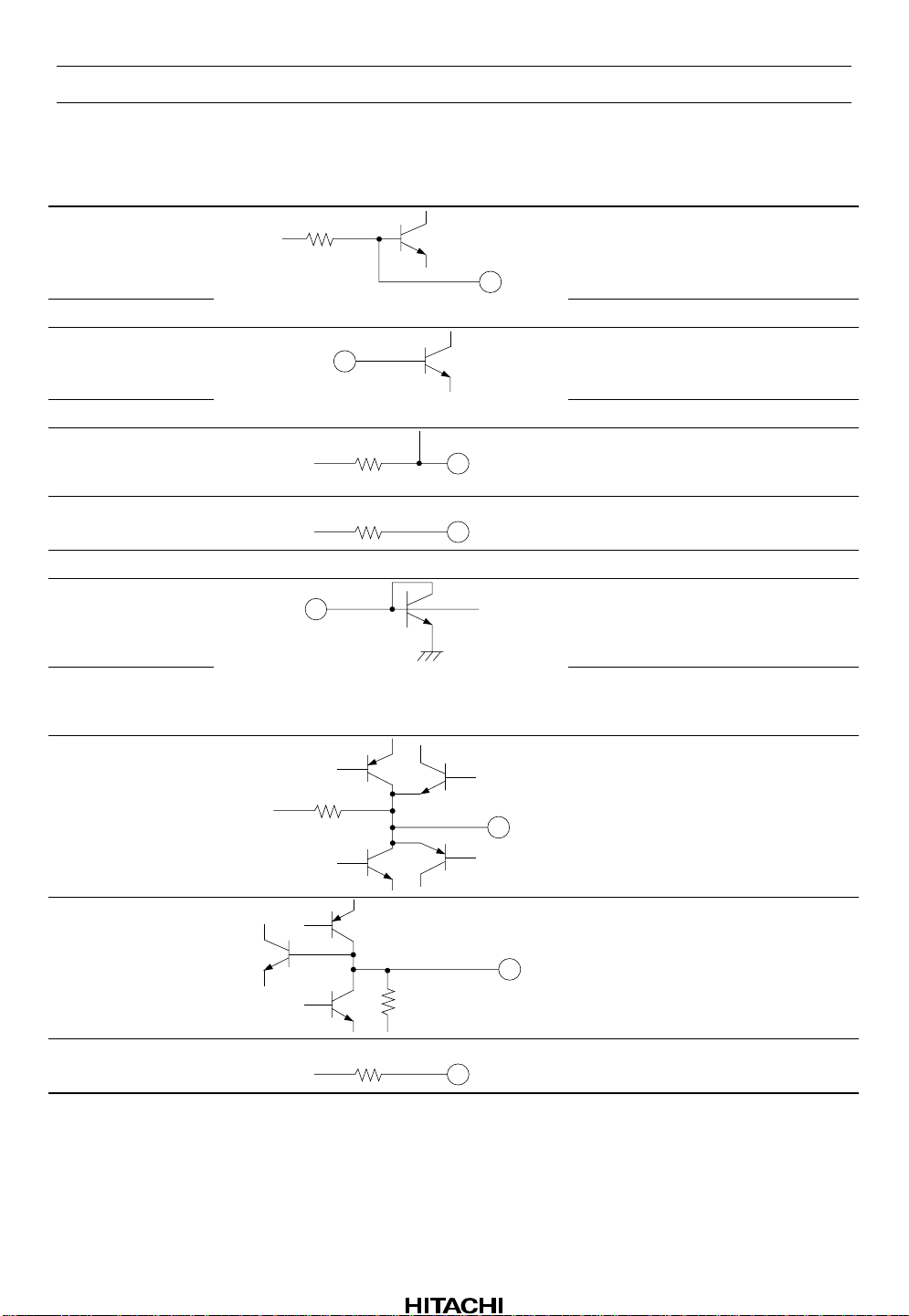
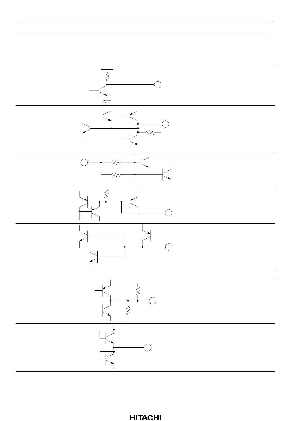
Pin Descriptions and Equivalent Circuits
Pin No. Symbol Equivalent Circuit Function
1FH
3 TH Tracking error hold signal output
2TSI Tracking servo input
56 FSI Focus servo input
4FLS
5 FLS
6 SGND — Servo ground
7 FPS Resistor connection for programming
470 k
90 k
30 k
Focus error hold signal output
Focus-servo low-frequency filter
resistor & capacitor connection
(FLS on)
Focus-servo low-frequency filter
capacitor connection (FLS off)
focus-servo phase compensation
(FPS off)
8 FPS Resistor connection for programming
focus-servo phase compensation
(FPS on)
9FSA
10 FS1
11 TLS
20 k
20 k
33 k
Focus servo output
FS1 voltage output
Tracking servo low-frequency filter
capacitor connection (TLS off)
Rev.1, Oct. 1995, page 3 of 35
Page 4
HA12188AF
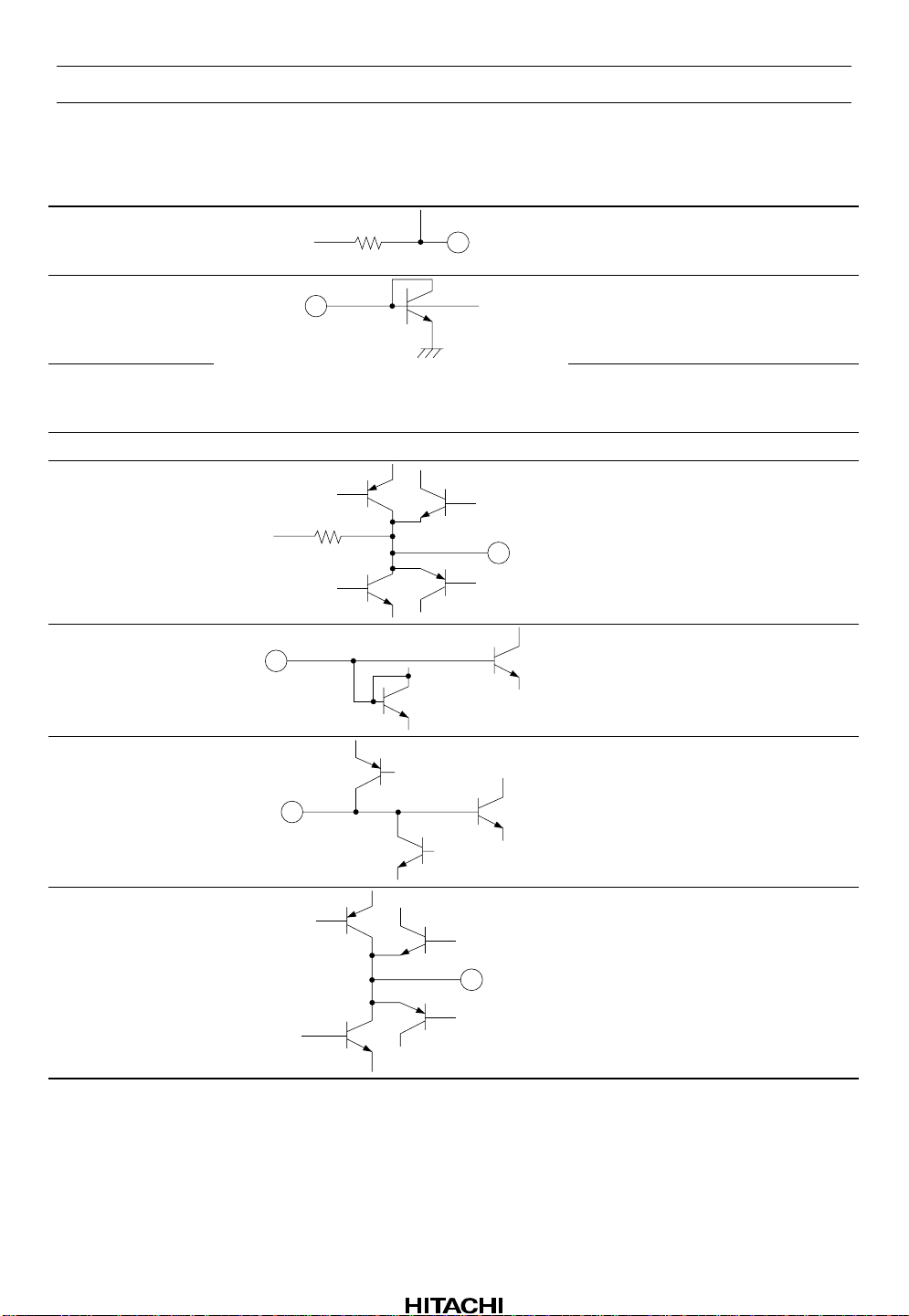
Pin Descriptions and Equivalent Circuits (cont)
Pin No. Symbol Equivalent Circuit Function
12 TLS
13 TPS Resistor connection for programming
14 TPS Resistor connection for programming
15 SV
16 TSA
CC
— Servo power supply
100 k
22 k
Tracking servo low-frequency filter
resistor & capacitor connection
(TLS on)
tracking servo phase compensat ion
(TPS off)
tracking servo phase compensat ion
(TPS on)
Tracking servo output
17 TM2 Sled serv o input
18 SSM SSA amplifier inverting input
19 SSA Sled servo output
Rev.1, Oct. 1995, page 4 of 35
Page 5
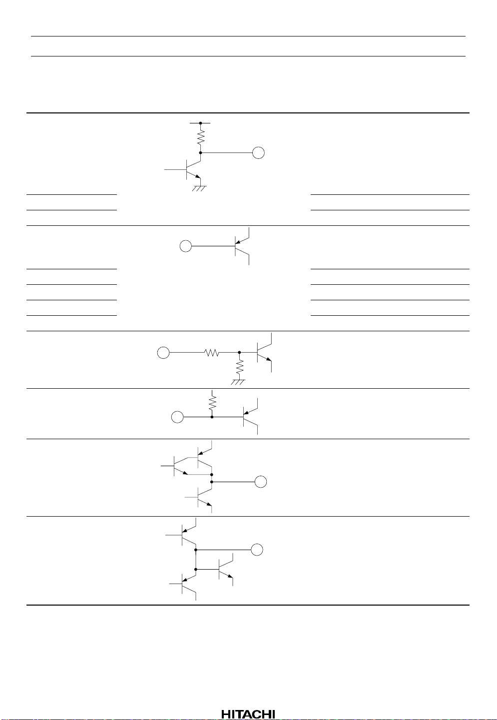
Pin Descriptions and Equivalent Circuits (cont)
Pin No. Symbol Equivalent Circuit Function
20 DRT
21 COUT COUT output
22 SENS SENS output
23 XRST Reset input
24 DC DC input
25 XLT XLT input
26 DATA Data input
27 CLK Clock input
28 LDS
10 k
50 k
V
CC
Defect signal output or inner/outer
direction signal output
Laser switch input
HA12188AF
50 k
29 DFIN
30 DFO Defect envelope signal output
31 DFH Defect hold signal output
43 k
Defect comparator input
Rev.1, Oct. 1995, page 5 of 35
Page 6
HA12188AF
Pin Descriptions and Equivalent Circuits (cont)
Pin No. Symbol Equivalent Circuit Function
32 FOK
V
CC
20 k
FOK comparator output
33 MIRH
100 k
34 RFA
35 BYPS
36 ISET Resistor connection for programming
37 PGND — Pre-amplifier ground
38 RFO
40 k
18 k
20 k
18 k
Mirror hold signal output
RF signal AC input
Capacitor connection for ripple filter
reference current
RF signal output
40 k
39 RS1 RS1 switch
Rev.1, Oct. 1995, page 6 of 35
Page 7
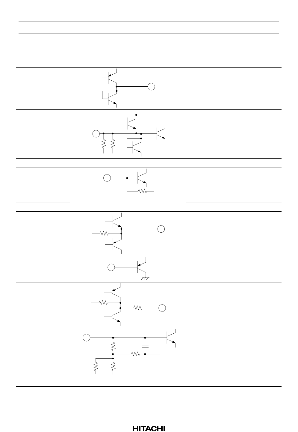
Pin Descriptions and Equivalent Circuits (cont)
Pin No. Symbol Equivalent Circuit Function
40 RS2
RS2 switch
HA12188AF
41 RFM
42 PV
43 RF1
5 k 5 k
CC
— Pre-amplifier power supply
10 k
RFS amplifier inverting input
RF1 amplifier input
44 RF2 RF2 amplifier input
45 V
C
20 k
Voltage reference output
46 MD APC amplifier input
47 LD
APC amplifier output
48 TR1
20 k
150 k
80 k
16 k
1 k
TR1 amplifier input
3.6 p
32 k
49 TR2 TR2 amplifier input
Rev.1, Oct. 1995, page 7 of 35
Page 8
HA12188AF
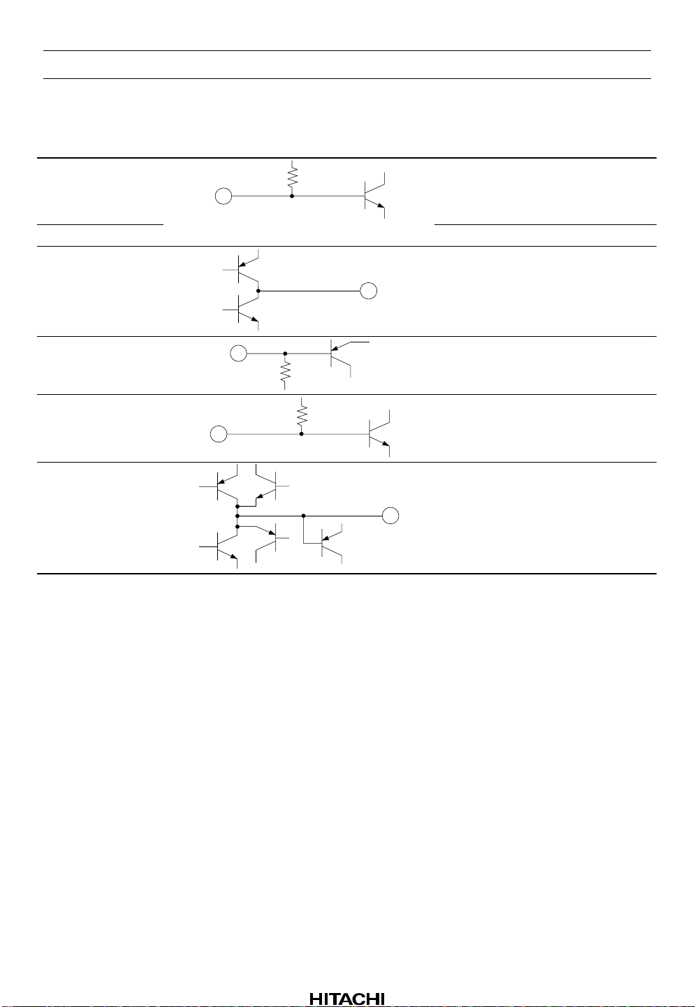
Pin Descriptions and Equivalent Circuits (cont)
Pin No. Symbol Equivalent Circuit Function
50 TEP
51 TEM TE amplifier inverting input
52 TEO TE amplifier output
22.6 k
TE amplifier non-inverting input
53 TZC
75 k
54 FAM
55 FAO FA amplifier output
5.5 k
TZC comparator input
FA amplifier inverting input
Rev.1, Oct. 1995, page 8 of 35
Page 9
HA12188AF
Operation
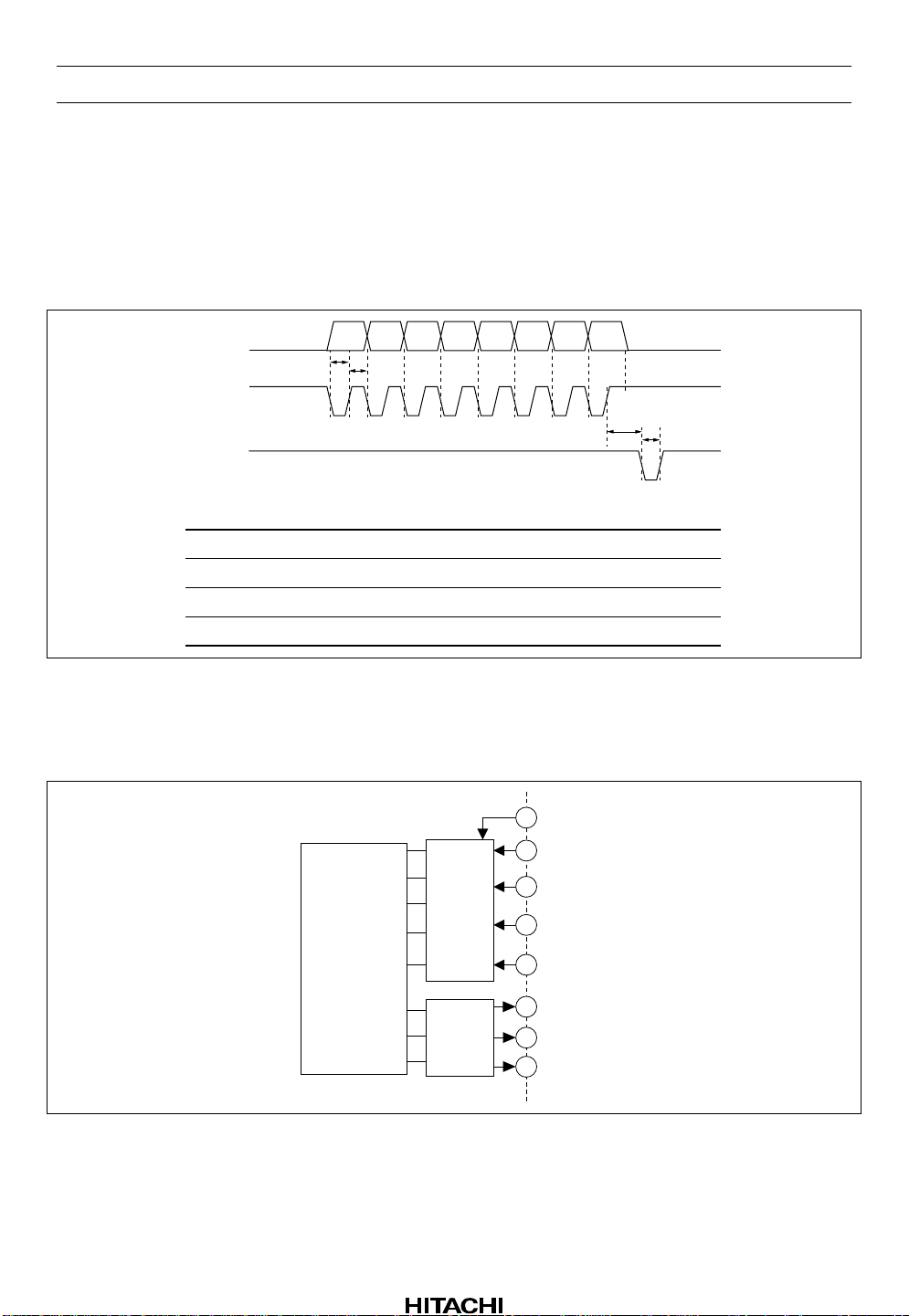
1. Microprocessor Control
The IC’s internal switches can be operated by sending control data from a microprocessor. The signal
timing is shown in figure 1, and the control commands are listed in table 1.
DATA
CLK
XLT
Item
Clock frequency
Clock pulse width
Delay time
Latch pulse width
01234567
T1
T2
Symbol
f
CLK
T1, T2
T3
T4
Min
—
0.96
1
2
Typ
—
—
—
—
T3
Max
520
—
—
—
T4
Unit
kHz
µs
µs
µs
Figure 1 Timing Diagram for Microprocessor Control
Signals from the microprocessor are input at pins 23 to 27. A low input at the XRST pin resets the IC.
Normally this pin should be kept high. (See figure 2.)
27
CLK
26
DATA
25
Input
I/F
Logic
Output
I/F
XLT
24
DC
23
XRST
22
SENS
21
COUT
20
DEFECT
or DRT
Figure 2 Microprocessor Interface
Rev.1, Oct. 1995, page 9 of 35
Page 10
HA12188AF
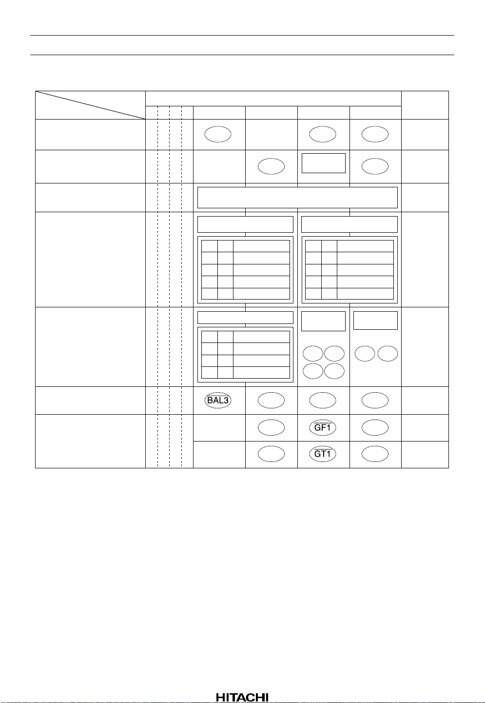
Table 1 Microprocessor Control Commands
D7D6D5D4 D3 D2 D1 D0
Focus mode
Tracking mode and FS1
DRT setting
0000
0001
FS4
*3
DRT
0: Defect
1: Direction
*1
DATA
DEFECT
OFF
*2
*4
TM7 THS H
FS2 FS1 FZC
FS1 current
*5
SENS
Access control mode
Pulse setting mode
Speed setting mode
EF balance adjustment
Tracking gain and focus
gain adjustment
Notes: 1.
The switch name surrounded by circle means that the switch turns on when the corresponding
bit is “1”. The switch name with bar surrounded by circle means that the switch turns on when
the corresponding bit is “0”.
“DEFECT OFF” means that switches DS1 and DS2 don’t turn on when the corresponding bit
2.
is “1”. Though the “DEFECT OFF” bit is set, the output at pin 20 is defect signal (in defect
signal output mode).
DRT (pin 20) outputs defect signal when the corresponding bit is “0”, and outputs direction
3.
signal when the corresponding bit is “1”.
TM7 can turn on only when COUT is high.
4.
The value of two current sources over switch FS1 are 18 µA(source) 36 µA(sink) when the
5.
corresponding bit is “1”, and are 9 µA(source) 18 µA(sink) when the corresponding bit is “0”.
The current values through switches TM3, TM4, TM5 and TM6 can be selected in four steps.
6.
The speed of Mirror circuit can be selected in three steps. Don’t use D3 = “1”, D2 = “0” mode.
7.
0010
0011
0100
0101
0110
D3
D3
0 ;
1 ; Tracking
D2
0
0
1
1
D2
0
0
1
Focus
gain
gain
0
1
0
1
0
1
1
Current value
Mirror
See table 2
*6 *6
32µA
16µA
24µA
8µA
*7
Mode
Normal
Double
Quadruple
BAL2 BAL1 BAL0 H
GF2 GF0 H
GT2 GT0
TM5, TM6 currentTM3, TM4 current
D1
D0
0
0
0
1
1
0
1
1
Focus
tracking
FLS FPS
TLS TPS
Current value
32µA
16µA
24µA
8µA
RF
RS1 RS2
TZC
H
H
H
Rev.1, Oct. 1995, page 10 of 35
Page 11
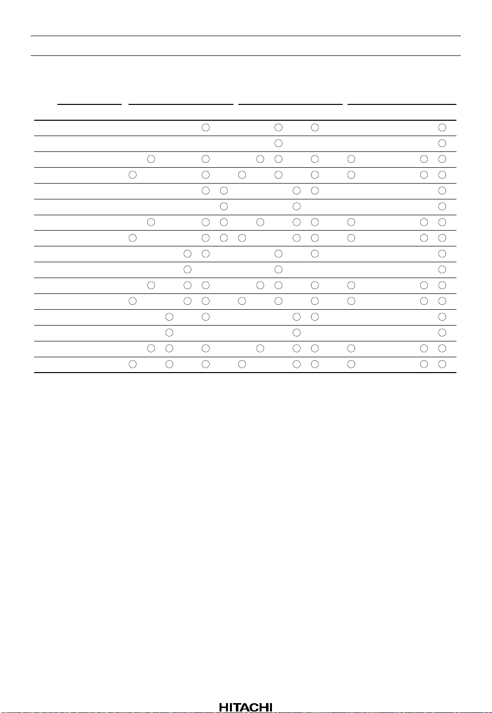
Table 2 Access Control Mode
HA12188AF
ST3
$20
$21
$22
$23
$24
$25
$26
$27
$28
$29
$2A
$2B
$2C
$2D
$2E
$2F
DATA ST1 ST2
D3
D2
D1
D0
0
0
0
0
0
0
0
1
0
0
1
0
0
0
1
1
0
1
0
0
0
1
0
1
0
1
1
0
0
1
1
1
1
0
0
0
1
0
0
1
1
0
1
0
1
0
1
1
1
1
0
0
1
1
0
1
1
1
1
0
1
1
1
1
TM5 TM4 TM3 TM2 TM1 TM6 TM5 TM4 TM3 TM2 TM1 TM6 TM5 TM4 TM3 TM2 TM1
TM6
A circle means that the switch is ON.
Note: After the microprocessor sends serial data, TM1 to TM6 can be switched among the states listed
under ST1 to ST3 by input at the DC pin. First, if the microprocessor sends serial data when DC is
high, TM1 to TM6 are placed in the state listed under ST1. When DC is brought low, the states
change to the states listed under ST2. Then if DC is brought high again, the states change to the
states listed under ST3.
Rev.1, Oct. 1995, page 11 of 35
Page 12

HA12188AF
Table 2-A Access Control Mode Appendix
1) Tracking servo
DATA Tracking servo movement
D3 D2 at DC = H (ST1)
0 0 Servo loop off
0 1 Servo loop on
1 0 Servo loop off jump to outside track
1 1 Servo loop off jump to inside track
2) Sled servo
DATA Sled servo movement
D1 D0 at DC = H (ST1)
0 0 Servo loop off
0 1 Servo loop on
1 0 Servo loop off move to outside track
1 1 Servo loop off move to inside track
Rev.1, Oct. 1995, page 12 of 35
Page 13

HA12188AF
2. RF and Focus Error Pre-Amplifiers
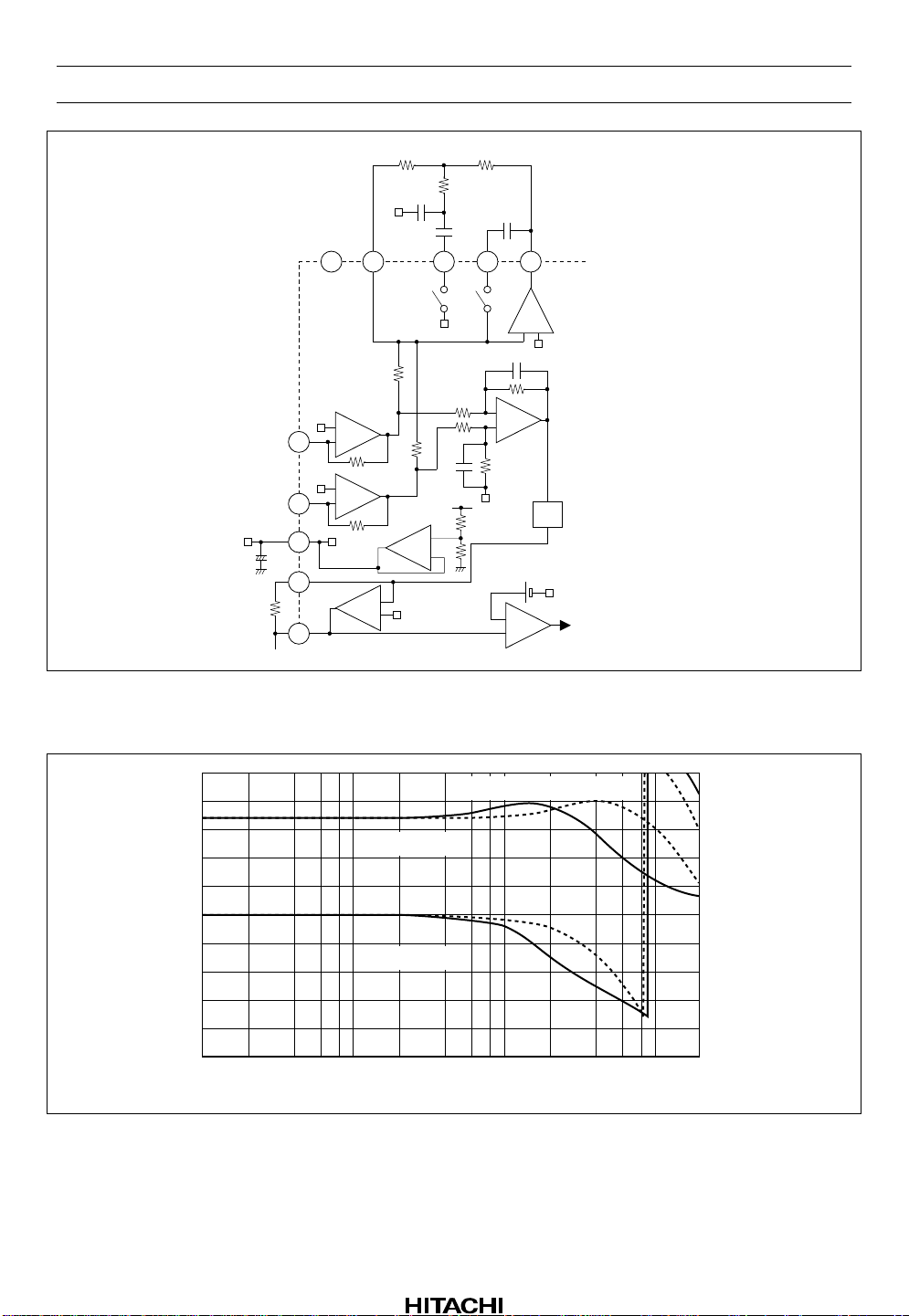
The main beam output signals from the photodiode IC are led in through resistors at pins 43 and 44. The
outputs of amplifiers RF1 and RF2 are summed by amplifier RFS to generate the EFM RF signal. (*1)
External resintances of pins 43 and 44 and amplifier RFS should be set according to the pick-up so that the
RF signal at pin 38 is about 1.5 V
voltage at no signal).
Switches RS1 and RS2 operate together under microprocessor control. For example they are on for normal
or double speed, and off for quadruple speed. ON resistance of RS1 is 1.1kΩ typ and on resistance of RS2
is 530Ω typ.
Figure 3-A shows the frequency characteristic at pin 38 in the condition of figure 3.(Input resistances of
pins 43 and 44 are 10kΩ.)
External resistances and capacitances should be fitted according to the pick-up. Stray capacitances of board
print patterns have influence on this frequency characteristic. Therefore external resistances and
capacitances should be set considering stray capacitances.
Amplifier FE subtracts the output of amplifier RF2 from the output of amplifier RF1 to generate the focus
error signal. The gain is 0dB. The focus error signal is output as the output of amplifier FA at pin 55, with a
gain set by variable resistor VR and the external resistance values. With the external resistors in figure 3,
the gain of amplifier FA is 8.7dB (initial value after reset).
(the difference between the peak level of 11T signal component and the
OP
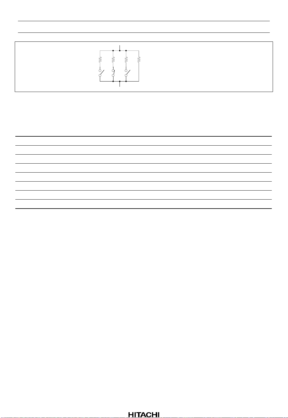
Variable resistor VR is controlled by 3-bit data. The gain can be varied from –5dB to +7dB with respect to
the reset value.
The focus error signal is binarized by comparator FZC, with a Vth equal to V
A reference voltage of 1/2 V
is output at pin 45. The IC’s internal reference voltage is connected
CC
+ 0.38V.
C
internally.
The feedback resistance of amplifier FA should be set according to the pick-up so that the focus S-curve at
pin 55 is about 3V peak-to-peak.
Note: 1 The sink current of amplifier RFS is about 1mA. When load capacitance of pin 38 is big because
of wiring with CD DSP LSI etc, please use buffer amplifier. (for example emitter follower
transistor)
Rev.1, Oct. 1995, page 13 of 35
Page 14
HA12188AF
100 µ
15 k
40
160 k
160 k
8.1 p
+
–
1.5 k
24 p
8.2 k
2 p
RS1
160 k
–
+
FE
160 k
–
+
3839
RFS
– +
8.1 p
VR
5.5 k
FZC
Unit R : Ω
C : F
1.8 k
22 p
V
CC
42
41
RS2
5 k
RF1
+
–
43
RF2
44
45
+
54
55
V
FA
5 k
10 k
+
–
10 k
C
–
+
Figure 3 RF and Focus Error Pre-Amplifiers
20
10
Gain
0
–10
Gain (dB)
Phase
–20
–30
10k 100k 1M 10M
Frequency (Hz)
RS1,2 ON OFF
2M 4M
Figure 3-A Frequency characteristic example of RF preamplifiers
180
144
108
72
36
0
–36
–72
–108
–144
–180
Phase (deg)
Rev.1, Oct. 1995, page 14 of 35
Page 15
HA12188AF
5.2 k 12.5 k 27.6 k
GF2 GF1 GF0
9.7 k
Unit R : Ω
Figure 4 Focus VR
Table 3 Focus VR and Gain
D2 D1 D0 VR Gain
0 1 0 9.7k –4.8dB
0 1 1 7.2k –2.2dB
0005.5k±0dB
0 0 1 4.6k +1.6dB
1 1 0 3.4k +3.8dB
1 1 1 3k +4.9dB
1 0 0 2.7k +6.0dB
1 0 1 2.4k +6.8dB
Rev.1, Oct. 1995, page 15 of 35
Page 16
HA12188AF
3. Tracking Pre-Amplifiers
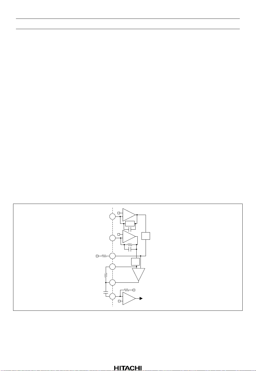
The sub-beam outputs from the photodiode IC are led in through resistors at pins 48 and 49.
External resistances of pins 48 and 49 and amplifier TE should be set according to the pick-up so that the
traverse signal at pin 52 is about 2 V
After a reset, the initial value of the feedback resistance BAL from amplifier TR1 to pin 48 is 400kΩ, the
same as the feedback resistance from amplifier TR2 to pin 49.
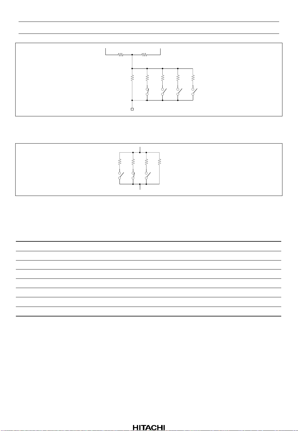
BAL has a variable resistance value that is controlled by 4-bit data. The variable range is from –32% to
+28% of the reset value. This resistance can be varied to adjust the EF balance of the tracking error.
Amplifier TE generates the tracking error signal. Its input signals are received from the preceding stage
through variable resistors VR. With the exter nal resistor values in figure 5, after a reset, the initial value of
the gain is 8.8dB.
The variable VR resistance is controlled by 3-bit data. The gain can be varied from –5dB to +7dB with
respect to the reset value.
The tracking error signal is coupled through a capacitor to input pin 53 and binarized by comparator TZC,
with a Vth equal to V
. (*1)
C
.
PP
Note: 1 At normal speed the output of amplifier TE contains much EFM signal components. Therefore
the output of amplifier TE had better be led in through LPF for reduction of EFM signal
components at pin 53.
TR1
+
–
48
BAL
TR2
3.6 p
62 k
49
50
+
–
3.6 p
VR
400 k
VR
51
62 k
52
0.022 µ
53
TE
75 k
+
–
– +
TZC
Unit R : Ω
C : F
Figure 5 Tracking Pre-Amplifiers
Rev.1, Oct. 1995, page 16 of 35
Page 17
80 k 32 k
20 k 40 k 80 k 160 k
16 k
HA12188AF
Unit R : Ω
BAL3 BAL2 BAL1 BAL0
Figure 6 BAL
21.7 k
51.7 k 114 k 40 k
GT2 GT1 GT0
Unit R : Ω
Figure 7 Tracking VR
Table 4 Tracking VR Values and Gain
D2 D1 D0 VR Gain
0 1 0 40k –4.9dB
0 1 1 29.6k –2.3dB
0 0 0 22.6k ±0dB
0 0 1 18.8k +1.6dB
1 1 0 14.1k +3.9dB
1 1 1 12.5k +4.9dB
1 0 0 11.1k +6.1dB
1 0 1 10.1k +6.9dB
Rev.1, Oct. 1995, page 17 of 35
Page 18
HA12188AF
Table 5 BAL Values
D3 D2 D1 D0 BAL Ratio
1 0 0 0 272k –32%
1 0 0 1 288k –28%
1 0 1 0 304k –24%
1 0 1 1 320k –20%
1 1 0 0 336k –16%
1 1 0 1 352k –12%
1 1 1 0 368k –8%
1 1 1 1 384k –4%
0 0 0 0 400k ±0%
0 0 0 1 416k +4%
0 0 1 0 432k +8%
0 0 1 1 448k +12%
0 1 0 0 464k +16%
0 1 0 1 480k +20%
0 1 1 0 496k +24%
0 1 1 1 512k +28%
4. FOK Detector
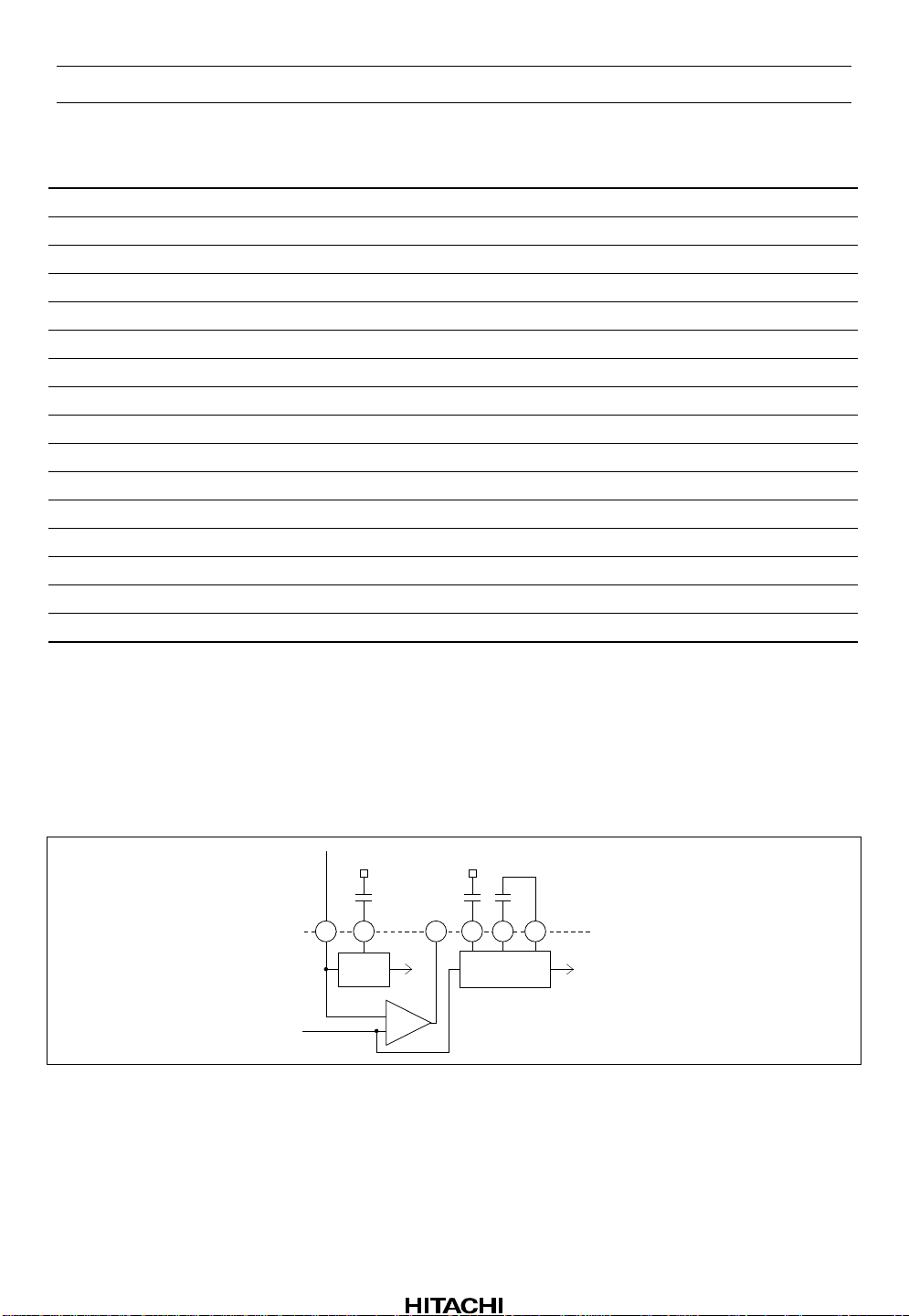
This detector is a comparator that generates the FOK signal. FOK is one of the signals that determines
when to activate the focus servo. When the voltage at pin 38 exceeds the voltage at pin 34 by
approximately 0.4V, pin 32 goes high.
Mirror
0.033 µ
FOK
–
+
0.015 µ
0.015 µ
3134 32 30 2933
Defect
Unit C : F
Figure 8 Mirror, FOK, and Defect Detectors
Rev.1, Oct. 1995, page 18 of 35
Page 19
HA12188AF
;
;
;
;
;
;
;
;;;;;;
;;;;;;
;;;;;;
5. Defect Detector
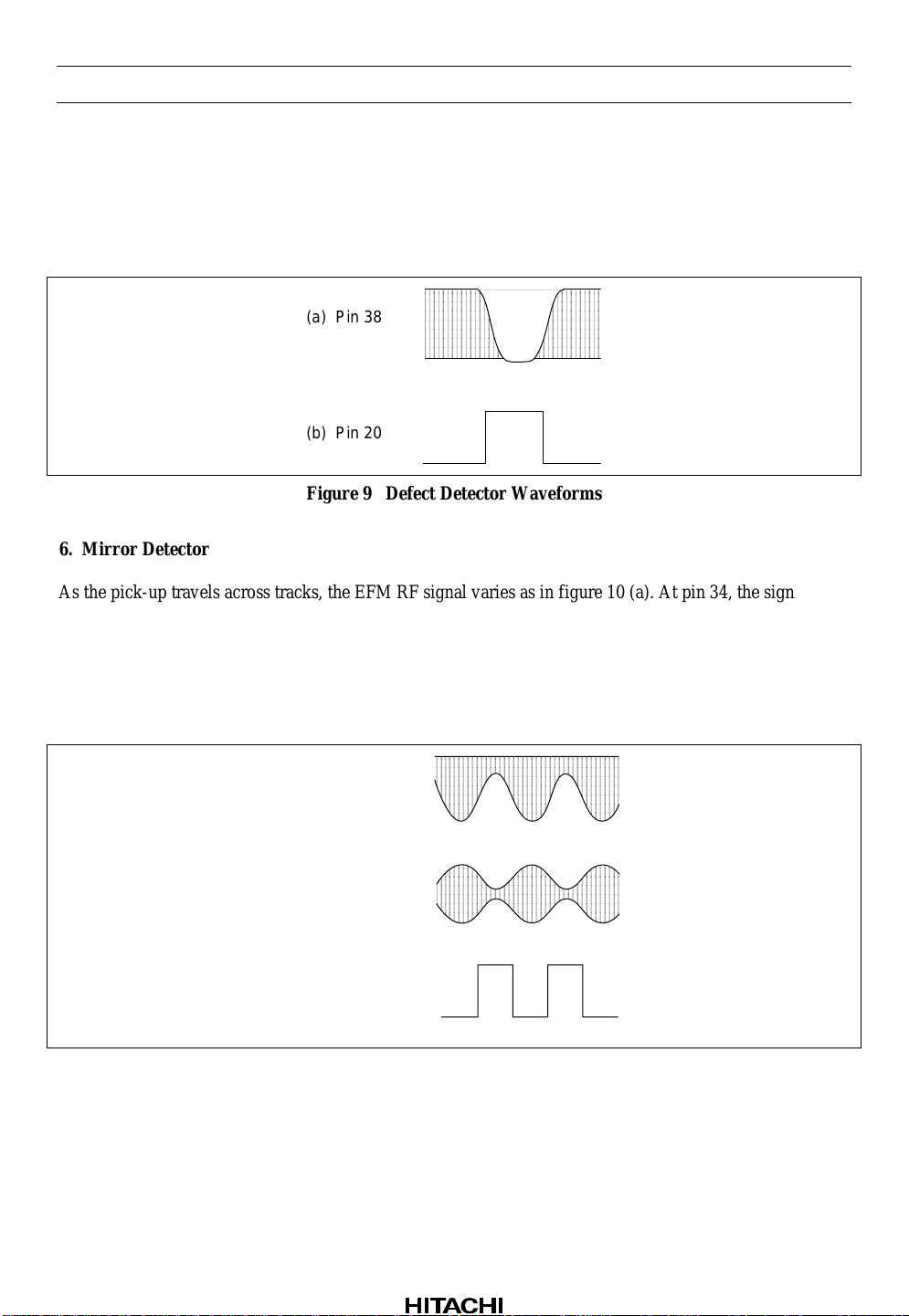
When a scratched disc is played, the EFM RF signal has the shape shown in figure 9 (a). The defect
detector detects the drop-out area of this signal. Scratches with dimensions of about 100µm or greater are
detected.
;;;;;;;;;;;;;;;;;;
;;;;;;;;;;;;;;;;;;
(a) Pin 38
(b) Pin 20
Figure 9 Defect Detector Waveforms
6. Mirror Detector
As the pick-up travels across tracks, the EFM RF signal varies as in figure 10 (a). At pin 34, the signal
varies as in figure 10 (b). The mirror detector detects the mirror areas. The external capacitor on pin 33
integrates the track-crossing frequency component.
;;;;;;;;;;;;;;;;;;
;;;;;;;;;;;;;;;;;;
;;;;;;;;;;;;;;;;;;
;;;;;;;;;;;;;;;;;;
;;;;;;;;;;;;;;;;;;
The internal time constant of the mirror detector can be set for normal, double, or quadruple speed by
microprocessor commands, to raise the trackable range of track-crossing frequencies.
(a) Pin 38
(b) Pin 34
(c) Mirror signal
(internal signal)
Figure 10 Mirror Detector Waveforms
Rev.1, Oct. 1995, page 19 of 35
Page 20
HA12188AF
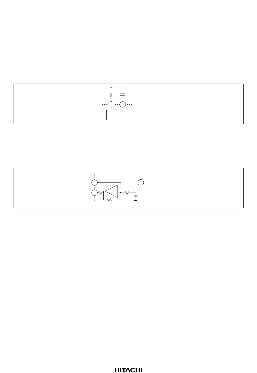
7. Bias
The 12-kΩ external resistor on pin 36 sets the reference value of the IC’s internal bias current. Use only
this resistance value. The IC will not operate correctly with o th e r resistance values.
Pin 35 is for a bypass capacitor to eliminate noise f r om the IC’s internal bias circuits.
Bias
0.1 µ
3536
Unit R : Ω
C : F
12 k
Figure 11 Bias
8. APC
This circuit is for the Psub laser diode. The APC circuit is switched off when pin 28 is high.
46
47
1 k
APC
+
–
28
LDS
Unit R : Ω
Figure 12 APC
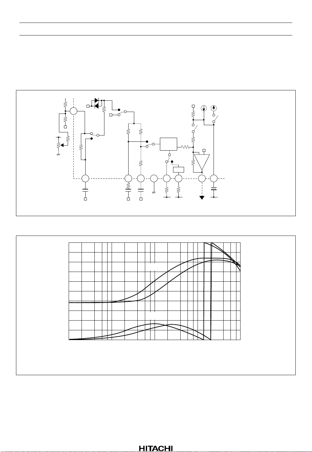
9. Focus Servo System
The focus error signal is led in through a gain-control resistor to pin 56. Focus bias is adjusted at pin 56.
When a defect is detected, switch DS2 propagates the focus error signal, which is integrated by an internal
resistor and external capacitor. Switch DS2 also inverts the phase of the propagated signal.
Switch FS4 is the focus servo loop switch.
Switch FLS switches low frequency filter , thereby switching the AC gain of the servo.
Switch FPS switches the peak phase-c ompensation frequency. This switch is linked with switch FLS and
tracking servo switches TLS and TPS. For example this switch is off at normal, double speed and is on at
quadruple speed.
The DC gain from input at pin 56 to output at pin 9 is 19dB. Figure 14 shows the frequency characteristic
when pin 4, 5 are open.
Rev.1, Oct. 1995, page 20 of 35
Page 21
HA12188AF
Switch FS1 switches a current sour ce to gener ate the focus search voltage. When switch FS2 is switched
on, focus is acquired by switching switch FS1 on and off.
The current through switch FS1 can be switched in two stages: 36µA sink/18µA source, and 18µA
sink/9µA source.
36µ/
18µ/
18µ
9µ
20 k
56
22 k
FS4
Focus
bias adj.
50
40
30
20
Gain (dB)
90 k
DS2
470 k
1 5
0.1 µ
4
91 k
0.047 µ
0.047 µ
Figure 13 Focus Servo
150 k
FLS
30 k
Gain
Phase
compen.
6
7
330 k 330 k
FPS
×2.7
8
FS2
20 k
FS1
7 k
FSA
– +
9
FAC
DRIV.
10
10 µ
+
Unit R : Ω
C : F
180
108
0
Phase (deg)
10
Phase
0
–108
–180
10 100k100 1k 2k 4k 10k
Frequency (Hz)
Note: Peak frequency of phase compensation is inversely proportional to external resistance value
(330kΩ at this figure) of pin 7, 8.(dot line : $40 mode, solid line : $42 mode)
Figure 14 Focus Servo Frequency Characteristic (pin 4, 5 are open)
Rev.1, Oct. 1995, page 21 of 35
Page 22
HA12188AF
The transform function of phase compen block at figure 13 is as follows.
–9
7.9×10
1+jω
VOUT
VIN
ø ≈ tan-1ω
8.95
≈
1+jω (2.7×10
7.9×10
()
at FPS OFF
or I8 ≈
I
7
–6
–9
I
I = I
External resistance value of pin 7 or 8
(
)
–tan-1ω
5.6×10
1+jω
(
5.6×10
()
7
V
– 0.71V
CC
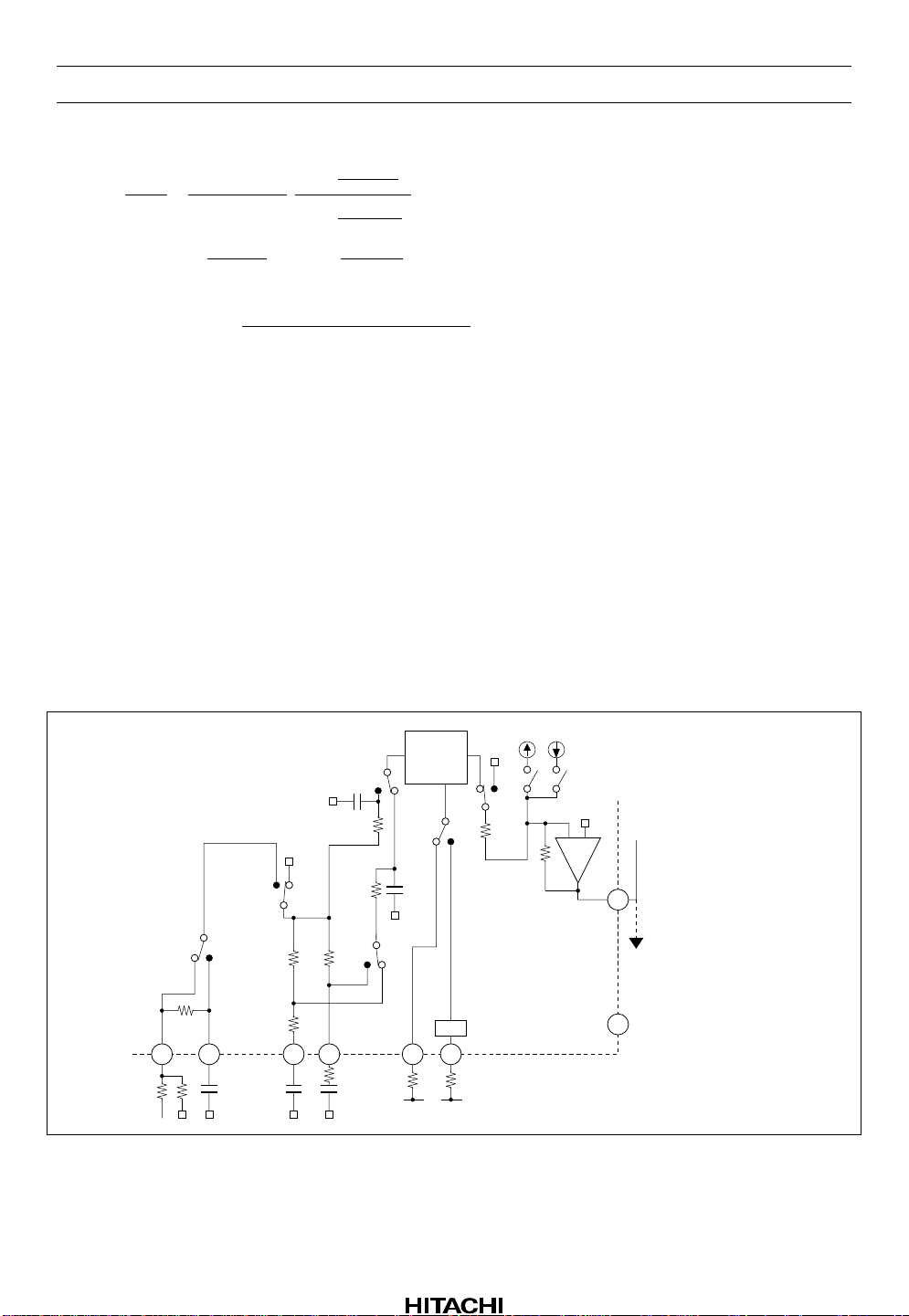
10. Tracking Servo System
The tracking error signal is led in through a gain-contr ol resistor to pin 2.
When a defect is detected, switch DS1 propagates the tracking error signal, which is integrated by an
internal resistor and external capacitor. Switch DS1 also inverts the phase of the propagated signal.
Switch TM1 is the tracking servo loop switch.
Switch TLS switches low frequency filter, thereby switching the AC gain of the servo.
The purpose of switch THS is to raise the high-frequency gain.
Switch TPS switches the peak phase-compensation frequency. This switch is linked with switch TLS and
focus servo switches FLS and FPS. For example this switch is off at normal, double speed and is on at
quadruple speed.
Switch TM7 is turned on by taking the logical AND of COUT and microprocessor data, to improve the
performance of the pick-up. COUT is a signal generated by latching Mirror with both edges of TZC.
)
I
–10
)
I
–10
–tan-1ω (2.7×10⁻⁶)
I
at FPS ON I = 2.7 I
8
THS
18 p
100 k
100 k
TM1
DS1
100 k
167 k
470 k
2
33 k
3 11 12 13 14
0.1 µ
0.1 µ
100 k
0.1 µ
Figure 15 Tracking Servo
Phase
compen.
18 p
TPS
TLS
×2.7
330 k 330 k
TM3 TM4
TM7
22 k
TSA
– +
16
15
TAC
DRIV.
V
CC
Unit R : Ω
C : F
Rev.1, Oct. 1995, page 22 of 35
Page 23
HA12188AF
50
40
30
Gain
180
108
0
20
Gain (dB)
10
0
Phase
–108
–180
Phase (deg)
10 100k100 1k 2k 4k 10k
Frequency (Hz)
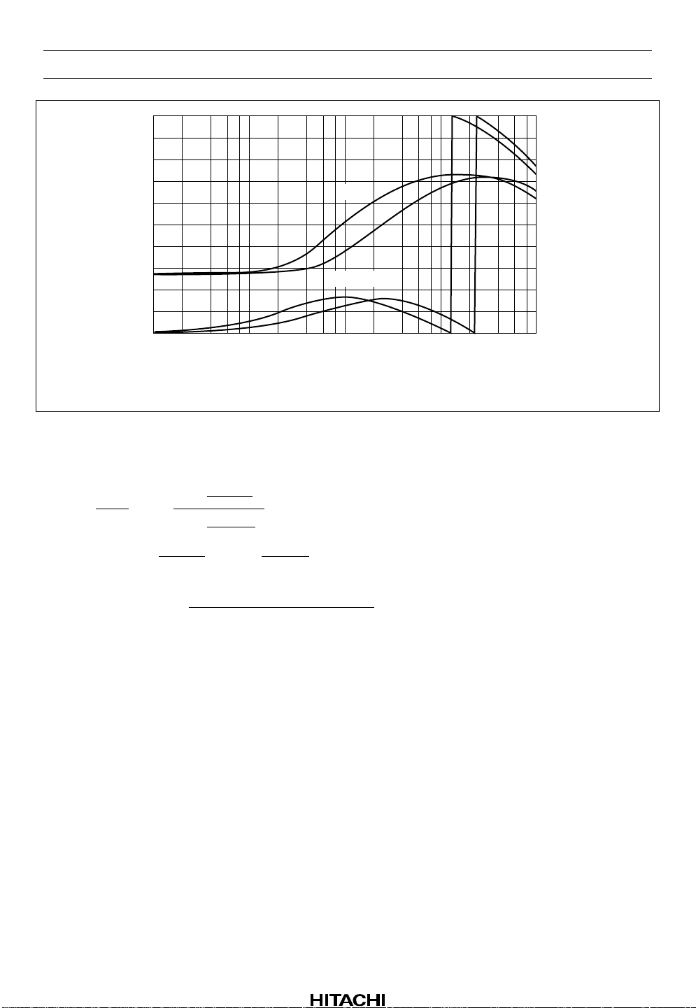
Note: Peak frequency of phase compensation is inversely proportional to external resistance value
(330kΩ at this figure) of pin 13, 14. (dot line : $40 mode, solid line : $42 mode)
Figure 16 Tracking Servo Frequency Characteristic (pin 11, 12 are open)
The transform function of phase compen block at figure 15 is as follows.
–9
7.9×10
1+jω
VOUT
≈ 4.47
VIN
ø ≈ tan-1ω
()
at TPS OFF at TPS ON
I13 or I14 ≈
(
5.6×10
1+jω
(
–9
7.9×10
I
I = I
External resistance value of pin 13 or 14
)
I
–10
)
I
–tan-1ω
5.6×10
()
13
V
– 0.71V
CC
–10
I
I = 2.7 I
14
Rev.1, Oct. 1995, page 23 of 35
Page 24
HA12188AF
;;;;;;;;;;;;;;;;;;;;;;;;;;;;;;;;;;;;;;;;;;;;;;;;;;;;;;;;;;
;;;;;;;;;;;;;;;;;;;;;;;;;;;;;;;;;;;;;;;;;;;;;;;;;;;;;;;;;;
;;;;;;;;;;;;;;;;;;;;;;;;;;;;;;;;;;;;;;;;;;;;;;;;;;;;;;;;;;
;;;;;;;;;;;;;;;;;;;;;;;;;;;;;;;;;;;;;;;;;;;;;;;;;;;;;;;;;;
;;;;;;;
;;;;;;;
;;;;;;;
;;;;;;;
;;;;;;;
;;;;;;;
;;;;;;
;;;;;;
;;;;;;
;;;;;;;;;;
;;;;;;;;;;
;;;;;;;;;;
;;;;;;
;;;;;;
;;;;;;
;;;;;;
;;;;;;
;;;;;;
;;;;;;;
;;;;;;;
;;;;;;;
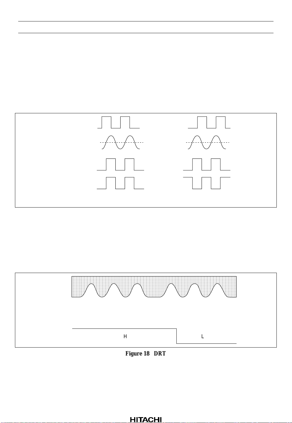
Figure 17 shows the phase relationships of Mirror, the tracking error, TZC, and COUT. TM7 operates to
prevent the moving direction component of the tracking error signal from reaching the actuator.
The purpose of switches TM3 and TM4 is to generate the track jump voltage. A positive vo ltage appears at
pin 16 when TM3 is switched on. A negative voltage appears at pin 16 when TM4 is switched on.
The current values through switches TM3 and TM4 can be selected in four steps: 8µA, 16µA, 24µA, and
32µA. The DC gain from input at pin 2 to output at pin 16 is 13dB. Figure 16 shows the frequency
characteristic when pin 11, 12 are open.
Mirror
Tracking error
TZC
COUT
(a) Moving inward (b) Moving outward
Figure 17 Phase Relationships of Mirror and Other Signals
11. DRT
DRT is an output signal that indicates the inward or outward direction. In the example in figure 18, DRT is
low during motion from outer toward inner tracks, and high for motio n in the reverse direction. This signal
is output from pin 20 on command from the microprocessor.
RF
(moving outward) (moving inward)
DRT
HL
Figure 18 DRT
Rev.1, Oct. 1995, page 24 of 35
Page 25
HA12188AF
12. Sled Servo
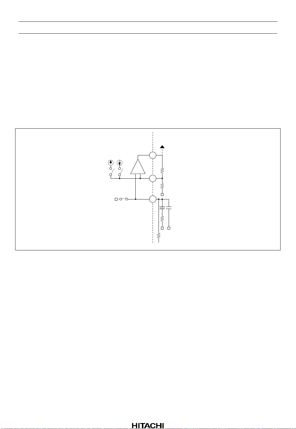
The signal output at pin 16 is passed through a lo w-pass filter and input at pin 17. TM2 is the loop switch
of the sled servo.
TM5 and TM6 are current switches that generate voltage s for large movements of the sled. A positive
voltage appears at pin 19 when TM5 is switched on. A negative voltage appears at pin 19 when TM6 is
switched on.
The current values through switches TM5 and TM6 can be selected in four steps: 8µA, 16µA, 24µA, and
32µA.
SLM
DRIV.
TM5 TM6
TM2
TM2 on resistsnce 230 Ω typ
SSA
–+
22
19
18
17
56 k
6.8 k
+
µ
82 k
0.22
12 k
µ
Unit R : Ω
C : F
Figure 19 Sled Servo
13. Direct Control
The switches in the tracking control and sled servo control blocks can be switched on and off by
microprocessor commands. TM1 to TM6 can also be controlled directly by the DC pin after input of serial
data from the microprocessor.
When the microprocessor sends a command from $20 to $2F as serial data with DC high, TM1 to TM6 are
placed in the states indicated under ST1 in table 2. Next, when DC is driven low, the states change to ST2.
When DC is brought high again, the states change to ST3.
Example of using the DC terminal for 1 track jump is as follows.
For inside track jump, after sending the $2C at DC = “H”, when the TZC’s rising edge is detected set DC =
“L” and set DC = “H” after a setting time.
For outside track jump, after sending the $28 at DC = “H”, when the TZC’s falling edge is detected, set DC
= “L” and set DC = “H” after a setting time.
Rev.1, Oct. 1995, page 25 of 35
Page 26
HA12188AF
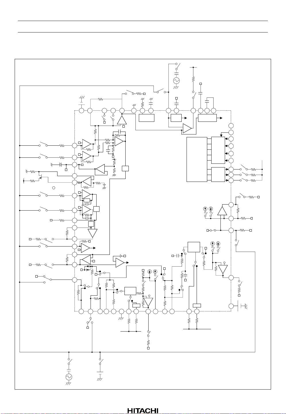
Test Circuit Diagram
V
CC
S43
S44
560
V
CC
2 k
S48
S49
39 k
S53
39 k
S56
2SB
561
S55
c
S52
10 µ
10 k
10 k
390 k
390 k
62 k
62 k
15 k
43
RF2
44
45
46
47
48
TR2
49
50
51
52
53
54
FA
55
56
S9
Bias
–
S34
0.1 µ
FS1
FSA
+
4.7 k
10 k
RS2
RF1
+
–
+
–
APC
+
–
TR1
+
–
BAL
+
VR
–
VR
–
+
TE
+
–
TZC
–
+
FS4
DS1
DS2
1 2 3 4 5 6 7 8 9 10 11
S2
S38
12 k
RFSRS1
– +
–
+
FE
+
–
VR
FZC
–
+
FLS
V
FS2
Phase
compen.
FPS
×2.7 ×2.7
200 k
CC
33 k
4 k7
Mirror
TM1
12
V
CC
S34A
0.1 µ
10 k
V
34
IN
S32
0.033 µ
FOK
–
+
Logic
Phase
THS
compen.
TLS
13 14
200 k 33 k
TPS
0.015 µ
Defect
TM7
0.015 µ
2930313233343536373839404142
Output
TM6TM5
TM2
V
CC
Input
I/F
I/F
TM4TM3
+
TSA
28
27
26
25
24
23
S22
22
S21
21
20
S20
S19
19
SSA
51 k
–
18
17
5 k 6
S17
–
+
16
S16
4 k7
15
V
CC
6 k2
10 k
4 k7
10 k
10 k
V
CC
S60
0.1 µ
60
V
IN
Rev.1, Oct. 1995, page 26 of 35
S61
V61
Unit R : Ω
C : F
Page 27

HA12188AF
Absolute Maximum Ratings
Item Symbol Value Unit
Power supply voltage V
Power dissipation P
CC
T
Operating temperature Topr –20 to +75 °C
Storage temperature Tstg –55 to +125 °C
Note: Recommended operating power supply voltage range: 5 ±0.5V.
7V
550 mW
Rev.1, Oct. 1995, page 27 of 35
Page 28

HA12188AF
Electrical Characteristics (Ta = 25°C, VCC = 5V)
Item Symbol Min Typ Max Unit Test Conditions Pins
1.Current dissipation I
2.Reference voltage V
RF amp. 3.Offset voltage V
4.Max. output level H V
5.Max. output level L V
6.Voltage gain G
Focus
7.Offset voltage V
CC
C
RF
RFH
RFL
VRF
FA
error amp.
Tracking
8.Max. output level H V
9.Max. output level L V
10.Voltage gain 1 G
11.Voltage gain 2 G
12.Offset voltage V
FAH
FAL
VFAI
VFA2
TE
error amp.
13.Max. output level H V
14.Max. output level L V
15.Voltage gain 1 G
16.Voltage gain 2 G
FOK 17.FOK Vth V
18.“H” output voltage V
19.“L” output voltage V
Defect 20.Max operation frequency F
21.Min operation frequency F
22.“H” output voltage V
23.“L” output voltage V
TEH
TEL
VTE1
VTE2
FOK
FKH
FKL
DH
DL
DFH
DFL
Note: All offset voltages are values referring to VC (pin 45)at XRST = “L”.
— 36 52 mA No signal 15, 42
2.3 2.5 2.7 V I45 = ±5mA 45
–65 0 65 mV 38
4.2 — — V S38,S43,S44,S61
38
V61 = 4.0V
— — 2.1 V S38,S43,S44,S61
38
V61 = 1.0V
10.0 12.0 14.0 dB S43, S44, S60
V38/V
60
IN
38
–65 0 65 mV 55
4.0 4.5 — V S44, S55, S61
55
V61 = 4.0V
— 0.5 1.0 V S43, S55, S61
55
V61 = 4.0V
6.7 8.7 10.7 dB S43, S60
V55/V
IN
6.7 8.7 10.7 dB S44, S60
V55/V
IN
60
60
55
55
–50 0 50 mV 52
4.0 4.5 — V S49, S52, S61
52
V61 = 4.0V
— 0.5 1.0 V S48, S52, S61
52
V61 = 4.0V
7.0 9.0 11.0 dB S49, S60
V52/V
IN
7.0 9.0 11.0 dB S48, S60
V52/V
IN
0.25 0.38 0.50 V S34, S61
60
60
52
52
32
when V32 ≥ 4V
Min (V38 – V34)
4.7 — — V S34, S61 32
— — 0.4 V S32, S34, S61 32
2 — — kHz S43, S44, S60 20
— — 1 kHz S43, S44, S60 20
4.7 — — V 20
— — 0.4 V S20 20
Rev.1, Oct. 1995, page 28 of 35
Page 29

HA12188AF
Electrical Characteristics (Ta = 25°C, VCC = 5V) (cont)
Item Symbol Min Typ Max Unit Test Conditions Pins
Defect 24.Operation min input level V
25.operation max input level V
COUT 26.Max operation frequency F
27.“H” output voltage V
28.“L” output voltage V
CLK,
29.“H” input level V
DF1
DF2
CO
COH
COL
MH
DATA,
XLT, DC,
XRST
30.“L” input level V
APC 31.APC voltage V
32.TZC Vth V
33.FZC Vth V
Focus
34.Offset voltage V
ML
APC
TZC
FZC
FO
servo
amp.
Tracking
35.Max output level H V
36.Max output level L V
37.Voltage gain G
38.Search voltage 1 V
39.Search voltage 2 V
40.Offset voltage V
FOH
FOL
VFO
S1
S2
TO
servo
amp.
41.Max output level H V
42.Max output level L V
TOH
TOL
Note: 90deg phase differnce between VIN 34 and VIN 60.
0.75 — — VPP S43, S44, S60 20
— — 2.5 VPP S43, S44, S60 20
100 — — kHz S34A, S53, S60 *
1
21
Mirror Qudruple
mode
4.7 — — V 21
— — 0.4 V S21 21
4.0 — — V 23 to
27
— — 1.0 V 23 to
27
0.09 0.16 0.23 V 46
–40 0 40 mV S53, S61
53
Refer to V53
0.25 0.38 0.50 V S43, S61 55
–100 0 100 mV 9
4.0 4.5 — V S9, S56, S61
9
FS4 on, V61 = 1.0V
— 0.8 1.0 V S9, S56, S61
9
FS4 on, V61 = 4.0V
16.9 18.9 20.9 dB S56, S60
V9/V
60
IN
9
FS4, FLS, FPS on
–0.70 –0.51 –0.32 V F S 2 on
V9 – V
– V
FO
0.32 0.51 0.70 V FS2, FS1 on
V9 – V
– V
FO
C
C
9
9
–120 0 120 mV 16
4.0 4.5 — V S2, S16, S61
16
TM1 on, V61 = 1.0V
— 0.8 1.0 V S2, S16, S61
16
TM1 on, V61 = 4.0V
Rev.1, Oct. 1995, page 29 of 35
Page 30

HA12188AF
Electrical Characteristics (Ta = 25°C, VCC = 5V) (cont)
Item Symbol Min Typ Max Unit Test Conditions Pins
Tracking
43.Voltage gain G
servo amp.
44.TM3 voltage V
45.TM4 voltage V
Sled servo
46.Offset voltage V
amp.
47.Max output level H V
48.Max output level L V
49.Voltage gain G
50.TM5 voltage V
51.TM6 voltage V
SENS 52.“H” output voltage V
53.“L” output voltage V
LDS 54.“H” input voltage V
55.“L” input voltage V
Focus VR 56.VR gain 1 G
57.VR gain 2 G
58.VR gain 3 G
59.VR gain 4 G
TrackingVR60.VR gain 1 G
61.VR gain 2 G
62.VR gain 3 G
63.VR gain 4 G
VTO
TM3
TM4
SO
SOH
SOL
VS
TM5
TM6
SEH
SEL
LDH
LDL
FVR1
FVR2
FVR3
FVR4
TVR1
TVR2
TVR3
TVR4
11.4 13.4 15.4 dB S2, S60
TLS, TPS, TM1 on
V16/V
60
IN
0.51 0.71 0.89 V TM3 on
V16 – V
– V
TO
C
–0.89 –0.71 –0.51 V T M 4 on
V16 – V
– V
TO
C
–66 0 66 mV 19
4.0 4.5 — V S17, S19, S61
TM2 on V61 = 4.0V
— 0.8 1.0 V S17, S19, S61
TM2 on, V61 = 1.0V
17.3 19.3 21.3 dB S17, S60
TM2 on, V19/V
IN
0.55 0.85 1.10 V 16µA mode
TM5 on
V19 – V
– V
SO
C
–1.10 –0.85 –0.55 V 16µA mode
TM6 on
V19 – V
– V
SO
C
4.7 — — V 22
— — 0.4 V S22 22
3.5 — — V 28
——0.5V 28
–5.8 –4.8 –3.8 dB S43, S60
V55 / V
60 – G
IN
VFA1
–3.2 –2.2 –1.2 dB S43, S60
V55 / V
60 – G
IN
VFA1
2.8 3.8 4.8 dB S43, S60
V55 / V
60 – G
IN
VFA1
5.8 6.8 7.8 dB S43, S60
V55 / V
60 – G
IN
VFA1
–5.9 –4.9 –3.9 dB S48, S60
V52 / V
60 – G
IN
VTE2
–3.3 –2.3 –1.3 dB S48, S60
V52 / V
60 – G
IN
VTE2
2.9 3.9 4.9 dB S48, S60
V52 / V
60 – G
IN
VTE2
5.9 6.9 7.9 dB S48, S60
V52 / V
60 – G
IN
VTE2
16
16
16
19
19
19
60
19
19
55
55
55
55
52
52
52
52
Rev.1, Oct. 1995, page 30 of 35
Page 31

HA12188AF
Electrical Characteristics (Ta = 25°C, VCC = 5V) (cont)
Item Symbol Min Typ Max Unit Test Conditions Pins
BAL 64.BAL gain 1 G
65.BAL gain 2 G
66.BAL gain 3 G
67.BAL gain 4 G
68.BAL gain 5 G
Mirror 69.Operation min input level V
70.Operation max input
level
Test Method Notes
BA1
BA2
BA3
BA4
BA5
MI1
–4.2 –3.2 –2.2 dB S48, S60
V52/V
IN
–3.7 –2.7 –1.7 dB S48, S60
V52/V
IN
–3.2 –2.2 –1.2 dB S48, S60
V52/V
IN
–2.4 –1.4 –0.4 dB S48, S60
V52/V
IN
1.1 2.1 3.1 dB S48, S60
V52/V
IN
0.25 — — V
S34A, S53, S60
PP
60 – G
60 – G
60 – G
60 – G
60 – G
VTE2
VTE2
VTE2
VTE2
VTE2
Quadraple mode
V
MI2
——2.5VPPS34A, S53, S60
Quadraple mode
52
52
52
52
52
21
21
Item No. Notes
1 I15 (I15 means “current at pin 15”. Following expressions are same as this expression.)+ I42
2 V45 (V45 means “voltage at pin 45”. Following expressions are same as this expression.
These symbols mean DC voltage at DC measuring and AC voltage at AC measuring.)
3 V38 – V
C
4, 5 V38
6 20log (V38 / VIN60) VIN60 = 500kHz, 0.2 V
7 V55 – V
C
PP
8, 9 V55
10, 11 20log (V55 / VIN60) VIN60 = 4kHz, 0.5 V
12 V52 – V
C
PP
13, 14 V52
15, 16 20log (V52 / VIN60) VIN60 = 4kHz, 0.5 V
PP
17 (V38 – V34) at the point that V32 exceeds 4V when V61 is lowered from 2.5V.
18, 19 V32
20 The maximum frequency for VIN60 such that the pin 20 signal is still a square wave.
60 = 0.25 VPP + VC + 95mV
V
IN
DC
21 The minimum frequency for VIN60 such that the pin 20 signal is still a square wave.
60 = 0.25 VPP + VC + 95mV
V
IN
DC
22, 23 V20
Rev.1, Oct. 1995, page 31 of 35
Page 32

HA12188AF
Test Method Notes (cont)
Item No. Notes
24 The minimum voltage for V38 such that the pin 20 signal is still a square wave.
60 = 1kHz + VC + 95mV
V
IN
25 The maximum voltage for V38 such that the pin 20 signal is still a square wave.
60 = 1kHz + VC + 95 mV
V
IN
26 VIN60, VIN34 90deg phase difference input signal VIN60 = VIN34 = 1 V
The maximum frequency for VIN60 (VIN34) such that the pin 21 signal is still a square wave.
27, 28 V21
29 H input voltage of pin 23 to 27
30 L input voltage of pin 23 to 27
31 V46
32 (V61 – V53) such that V22 exceeds 4V when V61 is upped from 2.4V. (SENS = TZC mode)
33 (V55 – VC) such that V22 exceeds 4V when V61 is upped from 2.5V. (SENS = FZC mode)
34 V9 – V
C
35, 36 V9
37 20log (V9 / VIN60) VIN60 = 1kHz, 0.15 V
38, 39 V9 – VFO – V
40 V16 – V
C
C
41, 42 V16
43 20log (V16 / VIN60) VIN60 = 1kHz, 0.3 V
44, 45 V9 – VTO – V
46 V19 – V
C
C
47, 48 V19
49 20log (V19 / VIN60) VIN60 = 4kHz, 0.15 V
50, 51 V19 – VSO – V
C
52, 53 V22
54 Input voltage of pin 28 such that APC is off.
55 Input voltage of pin 28 such that APC is on.
56 GF2 = 0, GF1 = 1, GF0 = 0 20log (V55 / VIN60) – G
57 GF2 = 0, GF1 = 1, GF0 = 1 20log (V55 / VIN60) – G
58 GF2 = 1, GF1 = 1, GF0 = 0 20log (V55 / VIN60) – G
59 GF2 = 1, GF1 = 0, GF0 = 1 20log (V55 / VIN60) – G
60 GT2 = 0, GT1 = 1, GT0 = 0 20log (V52 / VIN60) – G
61 GT2 = 0, GT1 = 1, GT0 = 1 20log (V52 / VIN60) – G
62 GT2 = 1, GT1 = 1, GT0 = 0 20log (V52 / VIN60) – G
63 GT2 = 1, GT1 = 0, GT0 = 1 20log (V52 / VIN60) – G
DC
DC
PP
PP
PP
PP
VIN60 = 4kHz, 0.5 V
VFA1
VIN60 = 4kHz, 0.5 V
VFA1
VIN60 = 4kHz, 0.5 V
VFA1
VIN60 = 4kHz, 0.5 V
VFA1
VIN60 = 4kHz, 0.5 V
VTE2
VIN60 = 4kHz, 0.5 V
VTE2
VIN60 = 4kHz, 0.5 V
VTE2
VIN60 = 4kHz, 0.5 V
VTE2
PP
PP
PP
PP
PP
PP
PP
PP
Rev.1, Oct. 1995, page 32 of 35
Page 33

HA12188AF
Test Method Notes (cont)
Item No. Notes
64 BAL3 = 1, BAL2 = 0, BAL1 = 0, BAL0 = 0 20log (V52 / V
60) – G
IN
65 BAL3 = 1, BAL2 = 0, BAL1 = 0, BAL0 = 1 20log (V52 / VIN60) – G
66 BAL3 = 1, BAL2 = 0, BAL1 = 1, BAL0 = 0 20log (V52 / VIN60) – G
67 BAL3 = 1, BAL2 = 1, BAL1 = 0, BAL0 = 0 20log (V52 / VIN60) – G
68 BAL3 = 0, BAL2 = 1, BAL1 = 1, BAL0 = 1 20log (V52 / VIN60) – G
69 The minimum input voltage for VIN34 such that the pin 21 signal is still a square wave.
60 = 1MHz, 1 VPP VIN34 = 100kHz
V
IN
70 The maximum input voltage for VIN34 such that the pin 21 signal is still a square wave.
60 = 1MHz, 1 VPP VIN34 = 100kHz
V
IN
VIN60 = 4kHz, 0.5V
VTE2
VIN60 = 4kHz, 0.5V
VTE2
VIN60 = 4kHz, 0.5V
VTE2
VIN60 = 4kHz, 0.5V
VTE2
VIN60 = 4kHz, 0.5V
VTE2
PP
PP
PP
PP
PP
Rev.1, Oct. 1995, page 33 of 35
Page 34
HA12188AF
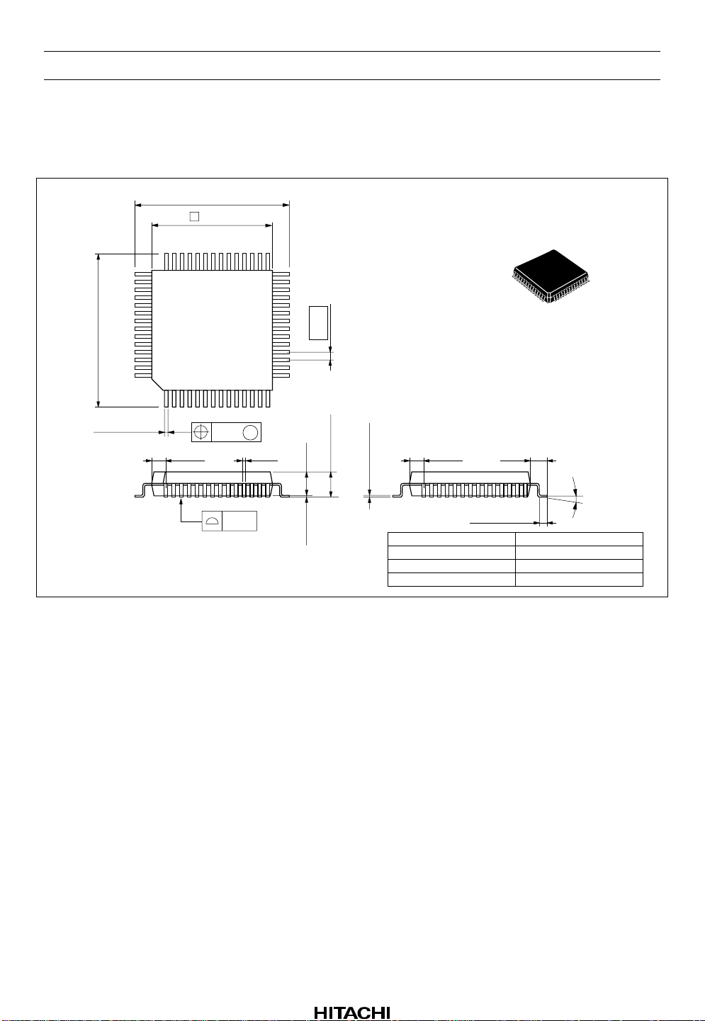
Package Dimensions
12.8 ± 0.3
42 29
Unit: mm
10.0
43
12.8 ± 0.3
56
0.32 ± 0.08
0.30 ± 0.06
28
0.65
15
M
0.35
14
2.20
+0.1
–0.09
0.1
2.54 Max
0.17 ± 0.05
0.15 ± 0.04
Hitachi Code
JEDEC Code
EIAJ Code
Weight
1
0.13
0.775 0.775
0.10
1.40
0 – 8˚
0.60 ± 0.15
FP-56
—
ED-7404A Mod.
0.51 g
Rev.1, Oct. 1995, page 34 of 35
Page 35

HA12188AF
Disclaimer
1. Hitachi neither warrants nor grants licenses of any rights of Hitachi’s or any third party’s patent,
copyright, trademark, or other intellectual property rights for information contained in this document.
Hitachi bears no responsibility for problems that may arise with third party’s rights, in cluding
intellectual property rights, in connection with u se of the information contained in this document.
2. Products and product specifications may be subject to change without notice. Confirm that you have
received the latest product standards or specifications before final design, purchase or use.
3. Hitachi makes every attempt to ensure that its products are of high quality and reliability. However,
contact Hitachi’s sales office before using the product in an application that demands especially high
quality and reliability or where its failure or malfunction may directly threaten human life or cause risk
of bodily injury, such as aerospace, aeronautics, nuclear power, combustion control, transportation,
traffic, safety equipment or medical equipment for life support.
4. Design your application so that the product is used within the ranges guaranteed by Hitachi particularly
for maximum rating, operating supply voltage range, heat radiation characteristics, installation
conditions and other characteristics. Hitachi bears no responsibility for failure or damage when used
beyond the guaranteed ranges. Even within the guaranteed ranges, consider normally foreseeable
failure rates or failure modes in semiconductor devices and employ systemic measures such as failsafes, so that the equipment incorporating Hitachi product does not cause bodily injury, fire or other
consequential damage due to operation of the Hitachi product.
5. This product is not designed to be radiation resistant.
6. No one is permitted to reproduce or duplicate, in any form, the whole or part of this document without
written approval from Hitachi.
7. Contact Hitachi’s sales office for any questions regarding this document or Hitachi semiconductor
products.
Sales Offices
Hitachi, Ltd.
Semiconductor & Integrated Circuits.
Nippon Bldg., 2-6-2, Ohte-machi, Chiyoda-ku, Tokyo 100-0004, Japan
Tel: Tokyo (03) 3270-2111 Fax: (03) 3270-5109
URL NorthAmerica : http://semiconductor.hitachi.com/
For further information write to:
Hitachi Semiconductor
(America) Inc.
179 East Tasman Drive,
San Jose,CA 95134
Tel: <1> (408) 433-1990
Fax: <1>(408) 433-0223
Europe : http://www.hitachi-eu.com/hel/ecg
Asia : http://sicapac.hitachi-asia.com
Japan : http://www.hitachi.co.jp/Sicd/indx.htm
Hitachi Europe GmbH
Electronic Components Group
Dornacher Straße 3
D-85622 Feldkirchen, Munich
Germany
Tel: <49> (89) 9 9180-0
Fax: <49> (89) 9 29 30 00
Hitachi Europe Ltd.
Electronic Components Group.
Whitebrook Park
Lower Cookham Road
Maidenhead
Berkshire SL6 8YA, United Kingdom
Tel: <44> (1628) 585000
Fax: <44> (1628) 585160
Hitachi Asia Ltd.
Hitachi Tower
16 Collyer Quay #20-00,
Singapore 049318
Tel : <65>-538-6533/538-8577
Fax : <65>-538-6933/538-3877
URL : http://www.hitachi.com.sg
Hitachi Asia Ltd.
(Taipei Branch Office)
4/F, No. 167, Tun Hwa North Road,
Hung-Kuo Building,
Taipei (105), Taiwan
Tel : <886>-(2)-2718-3666
Fax : <886>-(2)-2718-8180
Telex : 23222 HAS-TP
URL : http://www.hitachi.com.tw
Copyright Hitachi, Ltd., 2000. All rights reserved. Printed in Japan.
Hitachi Asia (Hong Kong) Ltd.
Group III (Electronic Components)
7/F., North Tower,
World Finance Centre,
Harbour City, Canton Road
Tsim Sha Tsui, Kowloon,
Hong Kong
Tel : <852>-(2)-735-9218
Fax : <852>-(2)-730-0281
URL : http://www.hitachi.com.hk
Colophon 2.0
Rev.1, Oct. 1995, page 35 of 35
 Loading...