

Page 1
DATE
28-Jan-99
I. These Techincal literature include materials protected under &he copyright of
Sharp
PIease do not reproduce or cause anyone to reproduce them without Sharp’s consent.
2. When using this product,
in these
for any damage
md the instructions included in these specification sheets, and the precautions
specification
resulting
please observe the absolut: maximum ratings
sheets, as well as the precautions mentioned below.
and the instructions for use outlined
Sharp assumes no responsibility
ficm use of the product which dces not comply with the absolute maxirn~m ratings
mentioned below.
(Precautions)
(1) This products is designed for use in the foUowing application areas;
l
0.4 equipment * Audio visual equipment * Home appliance
+ Telecommunication equipment (Terminal) l Measuring equipment
* Tooling machines * Compulers
I
If the use of the product in the above application areas is for equipment listed in paragraphs
(2) or (Z), please be sue to observe the precautions
given
in those respective paragraphs.
(2) Appropriate measures, such as fail-safe design and redundant design considering
the safety design of the overall system and equipment, should be taken to ensure reliability
and safety when &is product is used for equipment which demands high reliability and
safety in function and precision, such as ;
r l Transportation control and safety equipment
(aircraf?, aain, automobile etc.) 1 * Traffic sign& * Gas leakage sensor breakers l Rescue and security equipment
L
l Other
safety equipment
(3) Please do not use this product for equipment which require exnemeiy high rehability
and safety in function and precision, such 5s ;
r
l
Space equipment L * Telecommunication equipment (for trunk lines)
’ Nuclear power control equipment * hfedical equipment
(4) Please contact and consult with a Sharp sales representative if there are any questions
regarding interpretation of the
above three paragraphs.
3. Please contact and consult with a Sharp sales representative for any questions about
Corporation (“S’ha@).
7
I
_I
1
this
product.
** The technical literature is subject to be changed without notice **
Opto-Electronic Devices Division
Electronic Components Group
SH.AFW CORF’ORATION
Page 2
MOD& NJ.
G?viSWT95200A
DG-991015
1 Jan/T8/99
PAGE
l/13
17
GMSIn95200A technical
1. AppliCXian
Thi.~ technicat Litemure appk to the light en&kg diode
1
Chip
type white LED (GaN
2.
Outline dimensions and terminal
3.
Ratings and characteristics
chip LED device)
CO~UXC~~OCS
..,.................~.RefertotheanachedsheetPage2.
. . . . . . . . . . . . . . . . . . . . . . . . . ..‘..........
3-1. Absolute maximum ratings
3-2.
Electra characteristics
3-3.
Optical characteristics
3-1.
Ltious intensity rank
3-J.
Color coordinates ranks
3-6.
Derating curve
3-7.
Characteristics chart
4. Reliability
4-
1. Test items and test conditions
4-2. Failure judgement
5. Incomin_e inspection
5-1.
5-2. Description of inspection and
6. Taping specification
..,,...............I......... --.--..-.-.-...-.-......RefertotheattachedsheetPage6.
criteria
. . . . . . . . . . . . . . . . . . . . . . . . . . . . . . . . . . . . . . . . . . . .
Inspection method
criteria
..,........*,.................,...........*.
6-I. Taping
6-2. Label
6-3. Dampproof package
7.
Soldc.+g
7-1.
7-2.Mylual soldering
. . . . . . . . . . . . . . . . . . . . . . . . . . . . . . . . . . . . . . . . . . . . . . . . . . . . .
Reflow solderins
7-3. Dip soldering method
8.
Precsutions for use . . . . . . . . . a. . . . . . . . . .
-.......-.g...o.....,-..IRefer to &e attached beet Page 13.
8-l. Precautions maners for designing circuit
8-2.
Cleaning method
9. Environment
. . . . . . . . . . . . . . . . . . . . . . . . . . . . ..~....................
9-I. Ozonosphere destructive chemicals.
9-2. Brornic non-burning materials
Wrature
device MO&I NO.
Refer to the attached sheet Page 3-5
Refer to the attached sheet
Refer to the attached sheet Page 8-I 1.
Refer to the attached sheet
Refer to the attached shett Page 13.
GM5WT952oOA
Page 7.
Page 12.
Page 3
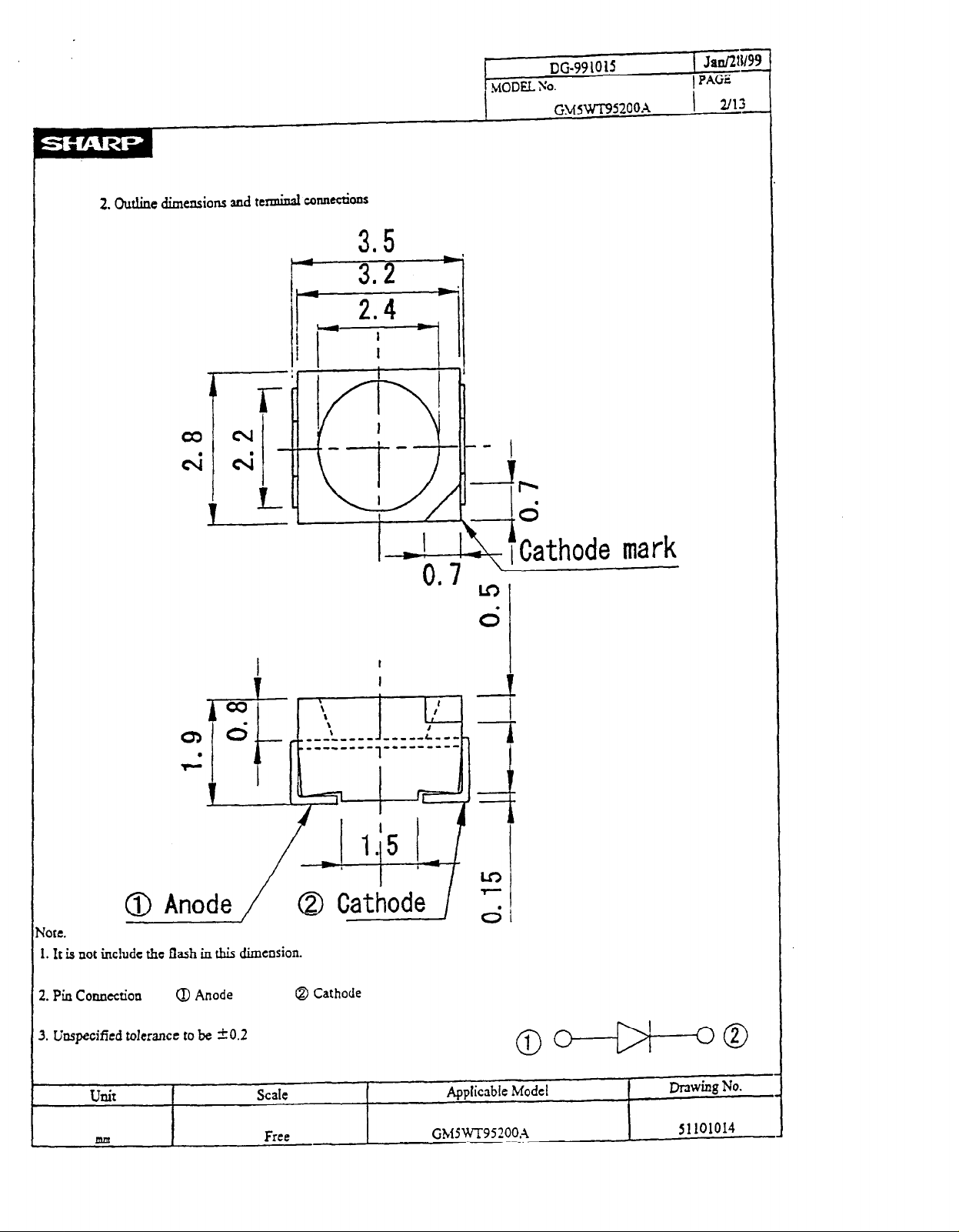
2. Outline dimensions and terminal connections
DG-991015
iMODEL X-a.
GM5WT352OOX
f-
.
1 Jan/21iii%-
) PAGE -
2J13
I -
0 Anode
N
‘OIC.
1
. It is not
2. Pin Connection
include the flash in this dimension.
I
!
I
-p+- \ ’ I
6 .,-.i __-- J _-_-- L,--
aa
.
P
-- IkL
---- -- 1 --------- Ql
3-L
I.2
0 Anode
/I-’ !.I
/ @ Cathode /
@ Cathode
I
~thade mark
Lo
T-
d
3. Unspecified tolerance to be k0.2
unit
BIB
Scale
Free
Applicable Model
Gbt5w-r95?00A
rhwhg No.
51101014
Page 4
c
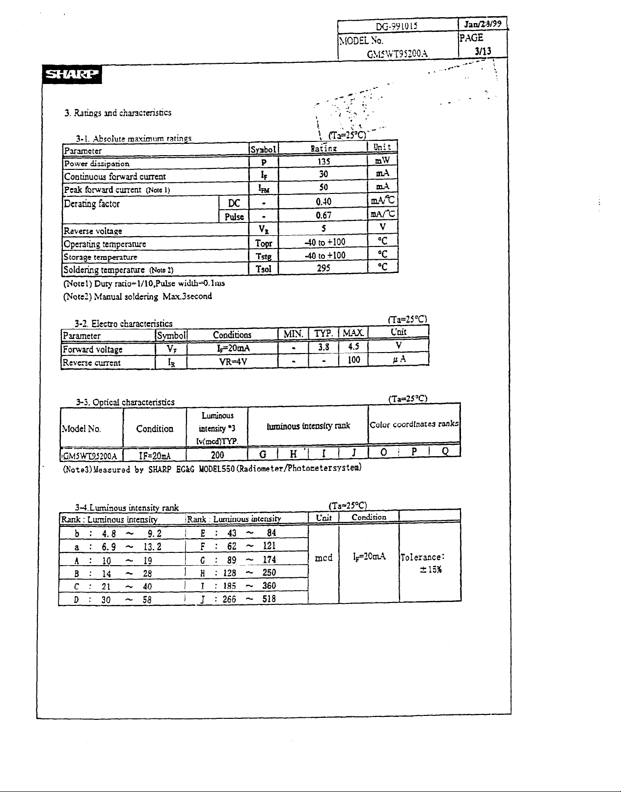
3.
Raiogs and charac:erktics
3-
1. Ahsolute maximum ratings
P3rameter
Power dissipation
Continuous fonvard current
Peak forward current @ore
Dcrating factor
Reverse voltage
Operating tempenture
Storage temperature
Soldering temperature
(Hotel) Duty ratio=1/10,Pulse width+.lms
(Note’) Manual soldering Max3second
1)
@ate 2)
(Syabol t
1 P I
IF
hl
DC -
Pulse I -
va
1 Topr 1
1 Tstg 1 40
1 Tsol 1 295
.- ’ .y- ’ : ;.
I
--~
30
50
0.10
0.67
5
40 to +100
to Cl00 1 oc
_ e-1--
--
_, -- .-
_, . .
.‘; -; ‘L .
. . ,-
.
IlLA
llL4
t&4x
IDA/t
1 v
( “C
1 “C
. ..-..-- ‘
..“-- .
. . .’
-
3-2. Elec&o characteristics
,
Parameter
Forward voltage
Reverse current 1s VR=4V w 1 100 I PA 1
3-3. Optid characteristics
I- 7
Model No. Condition intensity ‘3
--
GMSWT%?OOA
(NoteS)Ueasured by SHARP EGBG MODELS50 (RadiometerflhotonetersWem)
3d.Luminous intensity rank
Rank : Luminous
b : 4.8
a : 6.9 - 13.2
A : 10 - 19
8 : 14 - 28
c : 21 - 40
D : 30
/Symbol1
VF I&omt\
IF=20mX 200
intensity /Rank : Luminous intensity
- 9.2 j E : 43 - 84
-
;a
conditions
Luminous
luminous intensity ra&
Iv(mcd)TYP.
G(H’(I(J
/ F : 62 - 121
; i 1;; - 174
i
I I : 185 - 360
1 J : 266 - 518
- 250
1 MIN. lYP. 1 hf.4x.
1 - 3.8 1 4.5
,
1 Unit
mcd
(Ta=tS”C)
1 Lhit
1 V
Ta=T5’C)
-
color coordinates ranks
oiPlQ
olerance:
215%
Page 5
3-S.Color
coordilares ranks
Rank
0 0.26 - 0.32 1 0.2 - 0. 38
P
0
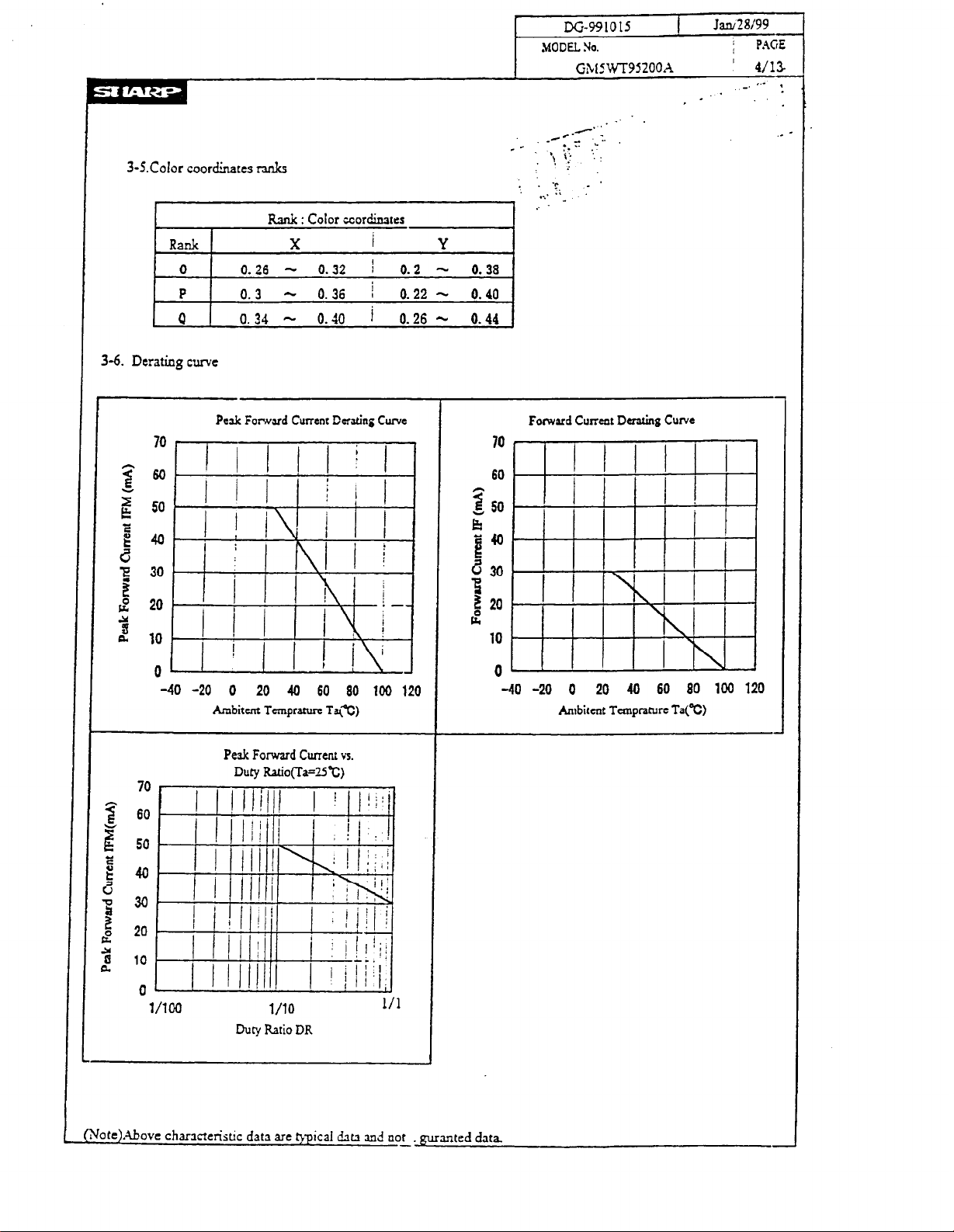
S-6. Derating curve
Rank :
Color coordinstes
X
I
Y
0.3 - 0.36 i 0.22 - 0. 40
0.34 - 0.40 ’ 0.26 - 0.44
DG-991015
.UODEL No.
GiLf5W95200A
c--
.- .-1.
_- :.= i’ .,
‘\ : .:
Jaw28199
j P.G’ 4/13
.;- .
, -
. .
. -.
“- 3
.-
-
Peak Forward Currenr Daating Cum
-40 -20 0
Ambittnr Tcmpraturc T$C)
Pelk Forward Current vs.
20 40 60 80 100
Dub Ratiofla=2%)
120
Fotward Current Dcrafing Curve
60
-40 -20 0 20 40 60 80 100 120
Ambitcnt Tanpraturo Tat%)
- l/lW
l/10
l/1
Duty Ratio DR
(Note Above charxteristic data are t)-pical km and not . gurvlted data
-
-
Page 6

3-7.
Characmistics chart
DG-991015 I
MCDEI. Ya
GMSWT952OOA
Sad2889 _
PACZ
5113
-
Relative Luminous Intesity vs. Fommd Cm
t.TaPt5Q
loooK
1% 0.
0. I
1 10 too
Forward Current I&4) Forward Voltage V,zo
Fonvard Cumt vs. Forward Vduge
1
2 3
. . . .
.‘i ..‘,I, .
;
i’;
I
. (‘.
G
-;*-.- - _ - .’
.. ‘.
.c .
i I_...- * -
w. -
(~~25’~
:
4
. .
5
n
[Aote)Above charxteristic data are typical data and not
gumted dam.
w-r95 _
Page 7

4. Rcliabiliry
The rcliabtity ofptoducrs shall be satisfied with items listed below.
DG-99lOU JaGG
hfODES No.
GSi5i-GT95200.A 6113
PAGE
4-1. Test items and :es concliricns
Test items
r
temperature cycling
Hieh temp’ and ‘@
humidicy storage
High temperature
storage
Low temper3rure
storage
Opcratig test
I
kfechtical shock
Vtiabte frequency
vibration
Soldering heat
5-2. Failure judgemeat criteria (Sotel)
Test conditions
-tO~C(jOmin)~+1OOt(3Omin),lCOCy
TazT6$C, NKRK, pI00Oh
Ta=(Tng-maximum ratings),r-1030h
Ta=(Tstg-minimun ratings),r IOCOh
Ta=25’C,Ie(IF-maximum ratings),~lOOOh
I
15 000m/s',0.5ms,3timesJ~X,iY~Zdirection
ZOOmis', 100-2
Refer to the attached sheetgage 12’13 1 time
OOO-100Wsweepfor ZOmin.,4times/yY,Z
Confidence level: 90%
S~plCS
n=22, c4
n=22,c=4 10
n=22, c-0 10
n=22,C=tl IO
~n=22,c=q 10
n=ll,C=o 20
direction
n=I 1, C-0 z”
n=ll,C=o 20
10
Parameter
r
Forward voltage
Reverse cuneat
Luminous intensity
fiote I)Mcasuring conditioa is in accordance with specification.
(Note2)U.S.L. is shown by Upper Specification Limit.
Symbol
VF
IR
IV
Iv > The
Fail judgement criteria (Noted)
v,> U.S.L. x I.2
I,> U.S.L. ' 2.0
first
stage value X 1.5 or The Jirst stage value X 0.5 > Iv
Page 8

DG-991015
MODEL So.
5. hcoming insptc5on
5-I. lrq-mion method
A single sampling pla normal inspection level II based on IS0 2859-I shail be adopted
- -. “M.*y.wU “I yuYb”LA”Y YUY .aI..‘a”
I JaanS
1 PAGE
NO.
inspection items
Criteria
1 Openhon No light emission
2
3
4
5
6
7
8 Resin ff ash
Radiation color Not cmreicl
Taping Product inserted in reverse direction
Label Model number is not printed,or misprinted
Electro-opcical
characteristics
Not conforming to the specification
Outline dimensions Not conforming to the specifhion
Dust and flaw Effect to the specification
-..-. -
0.3mm
or greater &om the product
Defect
AQL
gg 0.1%
Page 9

6. Taping
61 Taping
6-I-LShape and dimension of tapc(TYP.)
MODEL No.
GMSWI95200X
DG-991015
Janf2??i99
P?rGE
a13
Parameter 1 Symbol lDimension
1 Thickness 1 t , 0.3 I
Thickness of the entire tit 1 tt 1
2.3 (With cover
% Mated : Carrier titpe...PS, Cover tape...Polyestcr
tape
Remarks
and
carrier tape
combined
Page 10

6-I-t.Shape and dimension of reel(lYP
MODEL No.
I
GMSW95200X
DG-991015
1 9113
Parameter
Diameter
Frange
Hub
Jotation for part name etc.
% Material : Reel...Polystyrene
Thickness
Inner mace
EXtf
Emal diameter
Soindle hole diameter I C
Key slit f
I
direction
Width 1 E t r--
Depth
I
1 Symbol] Dimension 1 Remarks
rmm--.)
A d I78
t
w IO Dimensinn of shaft core
I
1 s q&o 1
) u t
(Labeling on one side of flange.@art name,quantity,Iot No.)
1.5
- --_--- ---- --
d13 t I
t
2.0
4.5
I
I
I
I
I
Page 11

6-I-3.Taping specification
(1) Lead tape:
End
DG-991015
MODEL No.
GM5WT95200A
~~11 out I-> Bigining
sanRa/99
PAGE
10113
Leading
10 plch or mare
Stuffed
Empty
10 pfi;h or nore ' 40-50 pith
(2) Cover tape stxngth against peeJing:F=O. 148N( 6 =lO”or less)
Cover taue
uuuuuuuduuuu
w Forward
Carrier tape
Tape speed : 5mm/s
(3) Tape strength against bending:
The rndius ofbendiug circle should be 30mm or more.
Lfit is less than 3Omm the cover may peel.
(4) Jointing of tape: There should not be joint
of
cover tape or carrier tape.
(5) Quantity per reel: Average 2,OOOpcs. per reel
(6) Product wcighr
Approx. 0.03 g
(7) others: 0 Ap parent defect of product ahorrId not be packed and product should not upset.
0 There should not be missing above continuous three products.
@ Products should be easily taken out.
@ Products should not be aaached to the cover tape at peeling.
6-2. Label for reel
C~lJwr9s20M
QUA.TY 2000
Lot number *--r
LOT No. KWBHOI
-=EIAJ C-3> WE M JAPAN
* :Lot number indication
0 Production plant code(to be indicated alphabetically)
@ Production Iot(single or double figures)
0 Year of productioa(tbe last two figures of the year)
@ Month of production
(to be indicated alphabeticaIly with Januuy corresponding to A)
0 Date of producdon(01 - 3 1)
- Model number
- Luminous rank and dominant waveIength rank
+ Production country
Page 12

6-3. Dampproof package
In other to avoid the absorption of humidir)i h tnnspo~ and storage.
the devices are packed in ahxninum sleeve.
r
Do-9910 15
MODELNo.
Label
GWWr952OOX
JwW99
PAGZ
11113
6-El.Strage conditions
Temperature : 5 to 30°C Humidity : less than 6O%RH
6-3-2.Treatment after opening
(1) Please make a soldering within 2 days ah opening under following condition;
Tempezmre : 5 co 30°C Humidity : less than 6O%RH
(2) In case the devices are not used for a long he after opening .the storage in dry box is recommendable.
Or it is
better
to repack he devices with a desicative by the sealer and put them in the some storage
conditions as 7-3- 1. Then they should k ?sed within 2 days.
(3) Please make a soldering afier a following h&king treatmeat if unused term should be over the conditions
of (2)
Reconunenclable conditions:
0 in taping
Temprature:6O”C to 65”C,Time:36 to AS hours
Q in individual (on PWl3 or metallic tray)
Tempmture: 100°C ,Time:2 to 3 houn
Page 13

7. Soldering
7-IRedow SOldeIiq
(1) It is
not
rc=ornmended to exceed the soidering temperarum and time
Caused by subsnare bend or the other mechanical stress &.ng reflow soldering
may happen gold wire disconnection etc. Therefore please
check
and study your
solder reflow machine’s best condition.
(2) Reflow soldering temperamre prome to be done under the following condition.
to be done under the following condition.
MAX 250
GM5%-i95200A
~IOWU
below.
1 1203
Time (s)
Recommendable Thermal Model
(4) Rccommcndable Metal Mask pattern for sLxen print
Recommend O.tmm to 03mm thickness metal mask
for screen print. Caused by solder reflow condition,
solder
paste, substrate and the other martial etc.,
my change solderbility.
Please check and study actual solderbihry before
usage.
Recommended solder pattern
7-2.Manual soldering
(1) It ia recommended to keep the soldering iron temperature at 295x (soldering iron
power ccnsumption 2Ow> and not to solder more than once or for over 3 seconds.
(2) When using a soldering iron, care must be taken not to damage the package.
(Pay attention not to allow any under stress or heat on package.)
7-3. Dip soldering method
To be done under the following condition.
Re-heat temp. : 80 to 120 “c
time : 30 to 120 seconds
Soldering temp. : Max. 260%
: within 5 seconds
time
Center of the product
Page 14

8. Precautions for use
8-1. Precautions matters for designing circuit
(l)This product is not designed as electromagnetic and ionized-particle
diari~n
resistant
UThis LED device applies blue LED & Borescent mattrial to emit white &ht. Therefore, dependhrg on the
vatue
of
operation current, tone of the color may channp slightly. Please check the tone under actual usage
condition in advance.
8-2. Cleaning method
(1) Solvent cleaning
Recommend conditions:
(2) Ultrasonic cIeaning
The affect on the device from ultrasonic bath, uIbasonic output, duration, board size and device mounting method.
Test the cleaning method under actual conditions and cheek for abnotmahties before aotual use.
(3) SoIVenb
Use only the folIowing types of solvent.
water, alcoho1, chIorofluorocabon-based solvent when c!eaning is necessary.
Recommend conditions: RT. 40KHz, 3OW/l, 3 to 5 minutes
9. Environrnenr
9-I. Ozonosphere destructive chemicals.
(I) The device doesn’t contain following substance.
(2) The device doesn’t have a production Line whose process requires foIlowing substance.
Restricted part: CFCa,haIones,CCI~,TtichIoroethane.(MethychIorofotm)
0 Solvent temperature is not more than 45 “c. @ Immersion up to 3 &mites.
9-Z. Bm& non-burning materials
The device doesn’t contain bromic non-burning materisIs(PBBOs,PBBs)
 Loading...