

Page 1
Features
GM0936TQ
GM0936TQ
Voice-Band Audio CODEC for CDMA
• Single 3-V operation
• Low power consumption
– Operating mode .... 20mW Typ
– Power-down mode ... 1mW Typ
• Combined A/D, D/A, and Filters
• Electret microphone bias reference
voltage available
• Compatible with all digital signal
processors (DSPs)
• Programmable volume control
• 300 Hz - 3.6 kHz Passband with Specified
Master clock
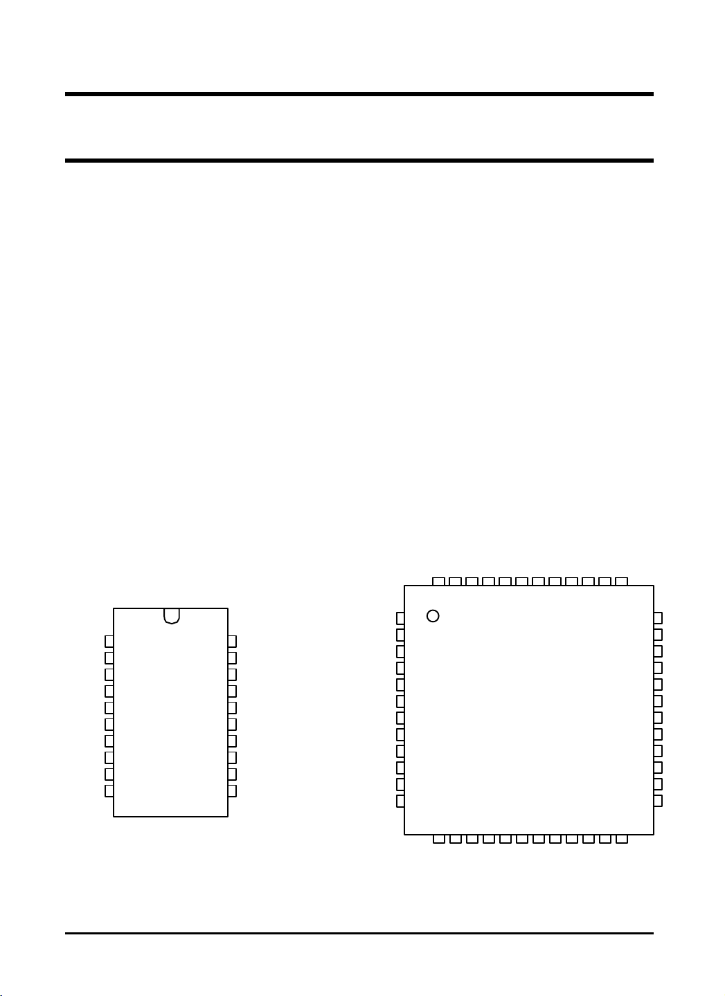
20 DIP/SOP
(TOP VIEW)
____
PDN
EARA
EARB
EARGS
Vcc
__________
MICMUTE
NC
DIN
FSR
__________
EARMUTE
1
2
3
4
5
6
7
8
9
10
20
19
18
17
16
15
14
13
12
11
MICBIAS
MICGS
MICIN
VMID
GND
NC
NC
DOUT
FSX
CLK
NC
NC
NC
AVcc
NC
NC
NC
NC
DVcc
NC
__________
MICMUTE
NC
• Designed for standard 2.048MHz master
clock for U.S. Analog, U.S. Digital, CT2,
DECT, GSM, and PCS Standards for
Hand-held Battery-Powered Telephones
• On-chip voltage references
• Package Type : 48 LQFP, 20 DIP, 20 SOP
48 LQFP
(TOP VIEW)
____
10
11
12
NC
NC
EARGS
484746
1
2
3
4
5
6
7
8
9
PDN
EARB
EARA
4443424140
45
MICIN
MICBIAS
MICGS
EXTMIC
MICSEL
38
39
NC
37
36
35
34
33
32
31
30
29
28
27
26
25
VMID
NC
AGND
NC
NC
NC
NC
NC
NC
DGND
NC
NC
131415
NC
NC
DIN
16
FSR
17
18
NC
CLK
__________
EARMUTE
20
21
23
24
FSX
22
NCNCNC
DOUT
19
1
Page 2

GM0936TQ
Description
The GM0936TQ contains A/D and D/A conversion functions integrated on a single chip, and utilizes
the sigma-delta modulation technique to achieve high resolution data conversion and low power
consumption. The GM0936TQ is an ideal analog front end device for high performance voice-band
communication systems. Cellular telephone systems are targeted in particular; however, these
integrated circuits can function in other systems including digital audio, telecommunications, and data
acquisition.
The transmit section is designed to interface directly with an electret microphone element. One of two
microphone input signals, MICIN and EXTMIC, is selected by MICSEL. If MICSEL is floated or
Low, then MICIN is selected, and if MICSEL is high, then EXTMIC is selected. The microphone input
signal (MICIN and EXTMIC) is buffered, first-order low-pass filtered, and amplified with provision for
setting the amplifier gain to accommodate a range of signal input levels. The amplified signal is 1bitmodulated by second-order sigma-delta modulator. The modulated signal is then applied to the input of
high-performance FIR-type digital decimation filters with frequency response equalization. The
resulting data is then clocked out of DOUT as a serial data stream.
The receive section takes a frame of sereal data on DIN and converts it to analog through highperformance FIR-type digital interpolation filter together with frequency response equalization,
second-order digital sigma-delta modulator, and analog reconstruction filters.
On-chip voltage reference ensures a highly integrated solution and all internal voltage references are
generated. An internal reference voltage, VMID, is used to develop the midlevel virtual ground for all
the amplifier circuits and the microphone bias circuit.Another reference voltage, MICBIAS, can supply
bias current for the microphone.
Serial DSP interfaces for transmit and receive paths support directly industry standard DSP processors.
The GM0936TQ devices are characterized for operation from -20 to 70¡É.
2
Page 3
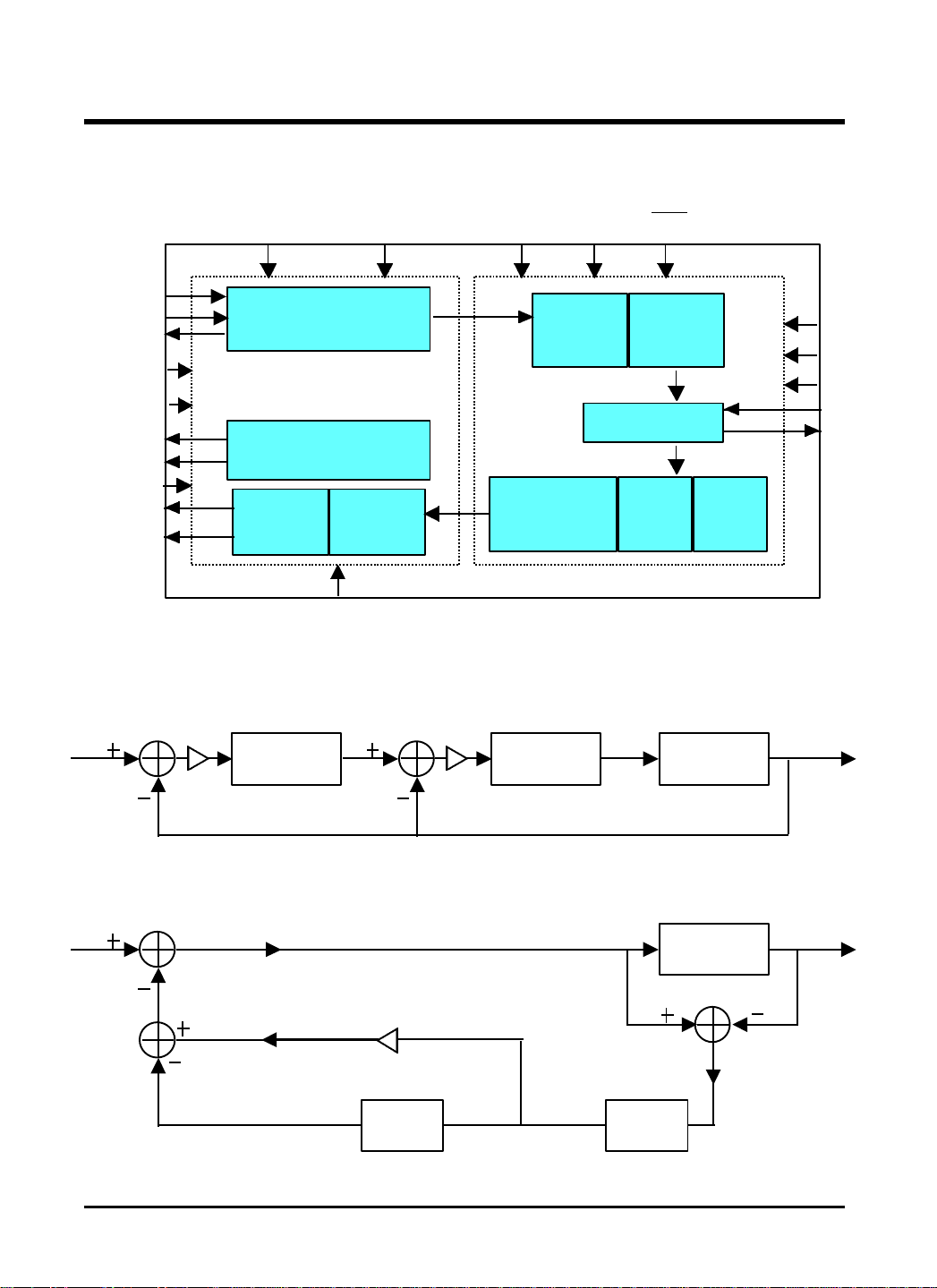
Block Diagram
AV
CC
AGND DV
CC
DGND
GM0936TQ
_ __
PDN
EXTMIC
MICIN
MICGS
__________
EARMUTE
MICMUTE
VMID
MICBIAS
EARGS
EARA
EARB
Analog 2nd orderΣ -
x
ANALOG
Σ ∆-MODULATOR
VOLTAGE
REFERENCE
POST
FILTER
∆
Modulator Block Diagram
1-BIT
DAC
MICSEL
Integrator1 Integrator2
DIGITAL Σ ∆-
MODULATOR
1/21/2
SINC 3FILTER
FIR-
FILTER
INTERFACE
SINC 2FILTER
Quantizer
CLK
FSR
FSX
DIN
DOUT
FIR-
FILTER
Y
Digital 2nd order Σ -
x
∆
Modulator Block Diagram
2
Quantizer
Y
Delay1Delay2
3
Page 4

Pin Description
LQFP
SOP&DIP
I/O
ANALOG SIGNALS
GM0936TQ
TERMINAL
NAME
AGND 34 16 Analog Ground
AVcc 4 5 Analog Power (3V)
EARA 44 2 O Earphone output
EARB 45 3 O Side-tone output
EARGS 46 4 I Side-tone input
EARMUTE_ 17 10 I Earphone output mute control signal
MICBIAS 42 20 O Microphone bias
MICGS 41 19 O Output of the internal microphone amplifier
MICIN 40 18 I Microphone input
MICMUTE_ 11 6 I Microphone input mute
VMID 36 17 O
ETMIC 39 N/A I Hand-free MIC-IN
DESCRIPTION
Bias voltage reference. A pair of external, lowleakage, high-frequency capacitors (1 µF and
470 pF) should be connected between VMID
and ground for filtering
MICSEL 38 N/A I
MIC-IN selection input. When float or
low, MICSEL selects MICIN. When high,
MICSEL selects EXTMIC.
4
Page 5

Pin Description
LQFP
SOP&DIP
I/O
1,2,3,
5,6,7,
12,13,
14,18,
22,23,
24,25,
26,28,
29,30,
31,32,
33,35
DIGITAL SIGNALS
GM0936TQ
TERMINAL
NAME
CLK 19 11 I Clock input (2.048 MHz)
DGND 27 16 Digital ground
DIN 15 8 I Receive data input
DOUT 21 13 O Transmit data output
DVcc 9 5 Digital power (3 V)
FSR 16 9 I
FSX 20 12 I
PDN_ 43 1 I Power-down input, Active Low
8,10,
NC
7, 14, 15 No internal connection
DESCRIPTION
Frame-synchronization clock input for
receive channel
Frame-synchronization clock input for
receive channel
5
Page 6
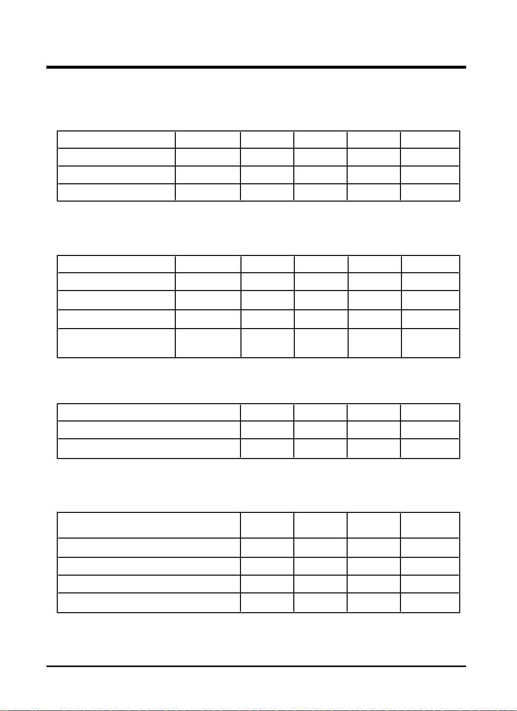
Electrical Characteristics
Absolute Maximum Ratings over operating free-air temperature range
GM0936TQ
SYMBOLPARAMETER MIN MAX UNIT
Supply Voltage Range V
Digital Input Voltage Range - 0.3 V
Analog Input Voltage Range - 0.3 V
DVCC,AV
V
ind
V
ina
CC
- 0.3 3.6
TYP
3.6
3.6
Recommended Operating Conditions
SYMBOLPARAMETER MIN MAX UNIT
Supply Voltage 3.3 V
High-level Input Voltage V
Low-level Input Voltage
Operating free-air
Temperature
Power Supply Characteristics, f
DVCC,AV
V
IH
V
IL
T
A
CC
2.2
-20 70
= 2.048 MHz, outputs not loaded, Vcc=3V, TA=25¡É
CLK
PARAMETER MIN MAX UNIT
TYP
3.02.7
0.8
TYP
V
¡É
Power Dissipation , Operating mW
Power Dissipation , Power down
Digital Characteristics (T
=25¡É , DVCC= AV
A
CC
= 3V)
PARAMETER MIN MAX UNIT
18
1
TYP
Input Capacitance 10 pF
Input Leakage Current - 10 10
Low-level output Voltage (IOL= 3.2mA) 0.4 V
High-level output Voltage (IOH= -3.2mA) 2.4 V
6
mW
§Ë
Page 7
Microphone interface
GM0936TQ
IIB Input bias current at MICIN
B1 Unity-gain bandwidth, open loop at MICIN
Av Large-signal voltage amplification at MICGS
Iomax Maximum
output current
VMID
TEST CONDITIONSPARAMETER MIN MAX UNIT
V I= 0 to 3 VVIO Input offset voltage at MICIN mV
TYP
1.5
10000
3
1MICBIAS(source only)
Speaker interface
TEST CONDITIONSPARAMETER MIN MAX UNIT
VO(PP) AC output voltage Vpp
IOmax Maximum output current
ro Output resistance at EARA, EARB
Gain change
RL = 600 Ω
EARMUTE low, max level
when muted
TYP
1
-60
+5
+200
3
+1
nA
MHz
V/V
µA
mA
mA
Ω
dB
7
Page 8

GM0936TQ
Analog Characteristics (T
=25¡É , DVCC= AVCC= 3V, fs = 8 KHz)
A
A/D Converter
PARAMETER MIN MAX UNIT
Oversampling Ratio
Resolution 13 bit
Dynamic Range
S/(N+THD)
Output Sample Rate 8 KHz
Maximum output current for MICBIAS 1 mA
Maximum output voltage for Microphone
Amplifier
50
0.85
TYP
128
70
52
0.95
dB
dB
Vpp
Transmit filter transfer over recommended ranges of supply voltage and free-air
temperature, CLK=2.048 MHz, FSX=8 kHz
MIN MAXUNIT
PARAMETER
TEST CONDITIONS
TYP
Gain relative to
input signal at
1.02 kHz
Input amplifier set for
unity gain, the output for
400mVpp signal at
MICGS is 0dB
fMICIN = 50 Hz
fMICIN = 200 Hz
fMICIN = 300 Hz
fMICIN = 1 kHz
fMICIN = 2 kHz
fMICIN = 3 kHz
fMICIN = 3.3 kHz
fMICIN = 3.8 kHz
8
0.76
0.73
0.67
0
-1.9
-4.5
-5.4
-8.9
dB
Page 9

GM0936TQ
Transmit idle channel noise and distortion, linear mode selected, over recommended
ranges of supply voltage and free-air temperature (see Notes 1 and 2)
MIN MAXUNIT
PARAMETER
Transmit noise
TEST CONDITIONS
MICIN connected to MICGS through a 22 kΩ resistor
TYP
178
µVrms
MICIN to DOUT at 0 dBm0
Gain relative to
input signal at
1.02 kHz
Notes: 1. The input amplifier is set for inverting unity gain.
2. Transmit noise, linear mode: 200 µVrms is equivalent to -75 dB (referenced to device 0 dB level).
MICIN to DOUT at -3 dBm0
MICIN to DOUT at -6 dBm0
MICIN to DOUT at -9 dBm0
MICIN to DOUT at -12 dBm0
53
52.3
51.9
50.7
49.0
D/A Converter
PARAMETER MIN MAX UNIT
Oversampling Ratio
Resolution 13 bit
Dynamic Range dB
S/(N+THD)
Maximum output current (RL=600§Ù)
Output Voltage Range Vpp
48
0.81
TYP
128
67
54
+ 1
0.91
dB
dB
mA
Receive distortion, linear mode selected, over recommended
ranges of supply voltage and free-air temperature
PARAMETER
Receive signal-to
-distortion ratio
with sine-wave
input
TEST CONDITIONS
DIN to EARA at 0 dBm0
DIN to EARA at -3 dBm0
DIN to EARA at -6 dBm0
DIN to EARA at -9 dBm0
DIN to EARA at -12 dBm0
9
MIN MAXUNIT
TYP
60
59.7
59.6
56.1
55.3
dB
Page 10

GM0936TQ
Power supply rejection over recommended ranges of supply voltage and operating
free-air temperature
PARAMETER MIN MAX UNIT
Supply voltage rejection,
transmit channel
Supply voltage rejection,
receive channel
Idle channel, supply signal = 100mVrms
f = 1 kHz (measured at DOUT)
Idle channel, supply signal = 100mVrms
f = 1 kHz (measured at EARA)
TEST CONDITIONS
TYP
-50
-50
dB
dB
10
Page 11

GM0936TQ
Timing (T
CLK Frequency
Sampling Rate 8 KHz
DIN Delay from CLK
=25¡É , DVCC= AVCC= 3V)
A
PARAMETER MIN MAX UNIT
TYP
2.048 MHz
35
35
Clock timing requirements
MIN NOM MAX
Duty cycle, CLK
45% 50% 55%
Transmit timing requirements
MIN MAX
nsDOUT Delay from CLK
ns
UNIT
UNIT
tsu(FSX) Setup time, FSX high before CLK ¡é
th(FSX) Hold time, FSX high after CLK ¡é
Receive timing requirements
tsu(FSR) Setup time, FSR high before CLK ¡é
th(FSR) Hold time, FSR high after CLK ¡é
tsu(DIN) Setup time, DIN high or low before CLK ¡é
th(DIN) Hold time, DIN high or low after CLK ¡é
20 468
20 468
MIN MAX
20 468
20 468
20
20
ns
ns
UNIT
ns
ns
ns
ns
11
Page 12

Timing Diagram
CLK
tsu(FSR)
FSR
15 16 15 16 1
GM0936TQ
Receive Time Slot
0 1 2 3 4 15 16 17
20%
80%
th(FSR)
20%
≈
80%
≈
See Note A
1 2
See Note B
3DIN
≈≈
4
See Note C
th(DIN)
tsu(DIN)
NOTES: A. This window is allowed for FSR high.
B. This window is allowed for FSR low.
C. Transitions are measured at 50%.
Figure1. Receive Side Timing Diagram
0 1 2 3 4 15 16 17
80%
CLK
tsu(FSX)
20%
th(FSX)
FSX
See Note A
DOUT
t
pd1
1 2
See Note C
Transmit Time Slot
≈≈≈≈
See Note B
t
pd2
3
4
20%
t
pd3
15 16
80%
NOTES: A. This window is allowed for FSX high.
B. This window is allowed for FSX low.
C. Transitions are measured at 50%.
Figure2. Transmit Side Timing Diagram
12
Page 13

GM0936TQ
PRINCIPLES OF OPERATION
power-down operation
To minimize power consumption, a power-down mode is provided.
For power down, an external low signal is applied to PDN. In the absence of a signal, PDN is
internally pulled up to a high logic level and the device remains active. In the power-down
mode, the average power consumption is reduced to 1mW.
Timing
FSX and FSR are inputs that set the sampling frequency. Data is transmitted on DOUT on the
positive transitions of CLK following the rising edge of FSX. Data is received on DIN on the
falling edges of CLK following FSR.
Table 1. Power-On and Power-Down Procedures
DEVICE STATUS
PROCEDURE
TYPICAL POWER
CONSUMPTION
DIGITAL OUTPUT STATUS
Power on
Power down
X = dont care
PDN =high,
FSX = pulses,
FSR = pulses
PDN =low,
FSX,FSR =X
20 mW
1 mW
Digital outputs active
DOUT in the high-impedance state
13
Page 14

GM0936TQ
PRINCIPLES OF OPERATION
transmit operation
microphone input
The microphone input amplifier is designed specifically to interface to electret-type microphone
elements, as shown in Figure 3. The VMID buffer circuit provides a voltage (MICBIAS) as a bias
voltage to the electret microphone. The microphone amplifier output (MICGS) is used in conjunction
with a feedback network and applied to the amplifier inverting input (MICIN) to set the amplifier gain.
VMID appears at a terminal to provide a place to filter the VMID voltage.
VMID
36
2.2 nF
22 kΩ
470 pF
MICBIAS
MICGS
MICIN
42
41
40
Microphone Amplifier
4.4 µF
2 kΩ
100nF
22 kΩ
Electret
Microphone
NOTE A: Terminal numbers shown are for the 48 LQFP package.
Figure 3. Typical Microphone Interface
VMID Reference
For Amplifiers
Reference
Voltage
Generator
To 2nd-order
Σ−∆ Modulator
GM0936TQ
microphone mute function
The MICMUTE input causes the digital circuitry to transmit all zero code on DOUT.
transmit filter
A low-pass antialiasing section is implemented by connecting a RC-pair externally between MICGS
and MICIN. The RC-pair, together with the microphone amplifier, provides a single-pole low pass
filter. The antialiased signal is 1bit-modulated by second-order sigma-delta modulator. The modulated
signal is then applied to the input of high-performance FIR-type digital decimation filters with
frequency response equalization.
14
Page 15

GM0936TQ
PRINCIPLES OF OPERATION
encoding
The encoder performs an A/D conversion on a 2nd-order Sigma-Delta (Σ-∆) modulator using a
switched-capacitor technology and high-performance FIR-type digital decimation filters with
frequency response equalization. The resulting data is then clocked out of DOUT as a serial data.
data word structure
The data word is 16 bits long. The first 13 bits comprises the audio data sample, and the last three bits
form the volume control word in the receive direction (DIN) and are zero pad bits in the transmit
direction (DOUT). The sign bit is transmitted first.
receive operation
decoding
The serial data word is received at DIN on the first 13 clock cycles. The receive section converts a
frame of sereal data to analog through high-performance FIR-type digital interpolation filter together
with frequency response equalization, second-order digital sigma-delta modulator, and analog
reconstruction filters.
receive buffer
The receive buffer contains the volume control.
earphone amplifier
The output can be used to drive a single-ended load with the output signal voltage centered around
VMID. EARA in Figure 4 is the output pin for the decoded analog signal. EARB in the figure is used
for sidetone signal output which is used internally. A resistor-capacitor pair attached to EARB is
embedded to reduce the number of on-board components. See the next section for more information on
sidetone generation.
15
Page 16

PRINCIPLES OF OPERATION
40 pF
GM0936TQ
50 kΩ
50 kΩ
VMID
30 kΩ
40 pF
30 kΩ
40 pF
GM0936TQ
NOTE A: Terminal numbers shown are for the 48 LQFP package.
VMID
100 kΩ
44
45
46
EARA
EARB
EARGS
Figure 4. Earphone Audio-Output Amplifier Configuration
receive data format
In the decoding operation, 16 bits of data are received. The first 13 bits are the D/A code, and the
remaining three bits from the volume control word(see Table 2). The volume control function is
actually an attenuation control in which the first bit received is the most significant. The maximum
volume occurs when all three volume control bits are zero. Eight levels of attenuation are selectable in
3-dB steps, giving a maximum attenuation of 21 dB when all bits are 1s. The volume control bit are not
latched into the GM0936TQ and must be present in each received data word.
16
Page 17

Table 2. Receive-Data Bit Definitions
BIT NO. Data
0 D12
1
2
3
4
5
6
7
8
9
A
B
C
D
E
F
D11
D10
D9
D8
D7
D6
D5
D4
D3
D2
D1
D0
V2
V1
V0
GM0936TQ
MSB
(sign bit)
D12 D11 D10 D9 D8 D7 D6 D5 D4 D3 D2 D1 D0 V2 V1 V0
PCM Data Volume Control
Time
Where:
D12-D0 = PCM Data word
V2, V1, V0 = Volume (attenuation control) 000 = maximum volume, 0 dB
LSB
111 = minimum volume, -21 dB
17
Page 18

GM0936TQ
APPLICATION INFORMATION
output gain set and sidetone considerations
The single-ended outputs EARA and EARB are capable of driving output power level up to 1mW into
load impedance of 1kΩ separately.The sidetone signal and the received signal can be summed by
configuring external components like in Figure 5. The amount of sidetone mixing is controlled by the
resistor connected between EARB and EARGS. If the resistance become greater, the amount of
sidetone mixing increases.
EARA
44
EARB
42
GM0936TQ
EARGS
46
41
MICGS
40
MICIN
NOTE A: Terminal numbers shown are for the 48 TQFP package.
To speaker driving amp.
1 kΩ
2.2 nF
22 kΩ
100 kΩ
22 kΩ
100nF
Electret
Microphone
Figure 5. Configuration for Gain-Setting and Sidetone
higher clock frequencies and sample rates
The GM0936TQ is designed to work with sample rates up to 16kHz where the frequency of the frame
sync determines the sampling frequency. However, there is a fundamental requirement to maintain the
ratio of the master clock frequency, f
, to the frame sync frequency, f
CLK
FSR
/ f
. This ratio for the
FSX
GM0936TQ is 2.048 MHz/8 kHz, or 256 master clocks per frame sync. For example, to operate the
GM0936TQ at a sampling rate of f
FSR
and f
equal to 16 kHz, f
FSX
must be 256 times 16 kHz, or
CLK
4.096 MHz. If the GM0936TQ is operated above an 8-kHz sample rate, however, it is expected that the
performance becomes somewhat degraded. Exact parameter specifications for rates up to 16-kHz
sample rate are not specified at this time.
18
Page 19

GM0936TQ
19
Page 20

GM0936TQ
20
Page 21

GM0936TQ
21
 Loading...