

Page 1

GDC21D401B
(Video Decoder)
Version 1.0
Mar, 99
HDS-GDC21D401B-9908 / 10
Page 2

GDC21D401B
The information contained herein is subject to change without notice.
The information contained herein is presented only as a guide for the applications of our products. No
responsibility is assumed by Hyundai for any infringements of patents or other rights of the third
parties which may result from its use. No license is granted by implication or otherwise under any
patent or patent rights of Hyundai or others.
These Hyundai products are intended for usage in general electronic equipment (office equipment,
communication equipment, measuring equipment, domestic electrification, etc.).
Please make sure that you consult with us before you use these Hyundai products in equipment which
require high quality and / or reliability, and in equipment which could have major impact to the welfare
of human life (atomic energy control, airplane, spaceship, traffic signal, combustion control, all types
of safety devices, etc.). Hyundai cannot accept liability to any damage which may occur in case these
Hyundai products were used in the mentioned equipment without prior consultation with Hyundai.
Copyright 1999 Hyundai Micro Electronics Co.,Ltd.
All Rights Reserved
3
Page 3

GDC21D401B
TABLE OF CONTENTS
1. General Description............................................................................................................5
2. Features...............................................................................................................................5
3. Pin Description....................................................................................................................6
4. Block Diagram...................................................................................................................10
5. Functional Description ..................................................................................................... 11
5.1 Initialization and Decoding Start...................................................................................11
5.2 Picture Decoding..........................................................................................................11
5.3 STC (System Time Clock) Generation..........................................................................12
5.4 DTS (Decoding Time Stamp) Synchronization..............................................................12
5.5 Error Concealment.......................................................................................................12
5.6 User Data Read............................................................................................................ 12
5.7 Bitstream Buffer Over/Underflow ..................................................................................13
5.8 VLD (Variable Length Decoder)....................................................................................13
5.9 Inverse Quantization ....................................................................................................13
5.10 IDCT (Inverse Discrete Cosine Transform).................................................................13
5.11 MC(Motion Compensation).........................................................................................13
5.12 Transport Interface.....................................................................................................14
5.13 Host Interface.............................................................................................................15
5.14 Video Data Output Format.......................................................................................... 20
5.15 Video Data Output Timing..........................................................................................21
5.16 SDRAM Interface .......................................................................................................22
6. Electrical Specification..................................................................................................... 24
6.1 Absolute Maximum Rating............................................................................................24
6.2 Recommended Operating Range .................................................................................24
6.3 DC Characteristics (VDD = 3.3 V±10%, TA = 0 ~ 70¡É)................................................24
6.4 AC Characteristics (VDD = 3.3 V±10%, TA = 0 ~ 70¡É) ................................................25
7. Package Mechanical Data.................................................................................................26
7.1 Package Pin Out .......................................................................................................... 26
7.2 Physical Dimension...................................................................................................... 29
4
Page 4

GDC21D401B
GDC21D401B
Video Decoder
1. General Description
The Video Decoder(VD) decodes video
elementary stream of MPEG-2(ISO/ICE
13818-2)MP@HL. It supports the ATSC
digital TV video standard, and can be used for
the video part of the ATSC digital TV with the
Transport Decoder and the VDP(Video
Display Processor). Picture decoding timing
can be controlled internally for A/V lip
synchronization, and externally for Video
Trick Mode by host microprocessor via I2C bus.
The Video Decoder can extract video user data
including caption from video elementary
stream, and host microprocessor can read the
video user data from the Video Decoder(VD)
via I2C. It uses four 16x1M SDRAMs and can
support up to 81 MHz memory clock speed.
2. Features
• Supports MPEG-2 (ISO/ICE 13818-2)
MP@HL
• Supports all video input formats of ATSC
digital TV standard
• Supports picture decoding capability up to
1920x1088 30 Frame/Sec
• Supports all kinds of motion compensation
methods of MPEG-2
• Supports MPEG-2 error code, syntax error
detection, and slice-based error concealment
• Supports DTS synchronization
• Supports VBV delay mode and low delay
mode decoding
• Supports film mode decoding (3:2 Pull
down)
• Supports high level commands for trick
mode
• Supports 8(w)x64(d) internal user data FIFO
• Outputs: macroblock format
4-pel parallel output
54 MHz synchronous I/F
Data window (pdwin, sclk, and mbclk)
Picture information (Picture structure, Field
parity, and DCT type)
• External memory for VBV buffer , DTS
FIFO and 2-frame memory:
64-bit Data Bus
81 MHz Synchronous Interface
64-Mbyte
Four 16x1M SDRAMs
• Host processor interface: I2C bus interface
Two interrupt signals
Supports 23 programmable internal
registers
5
Page 5
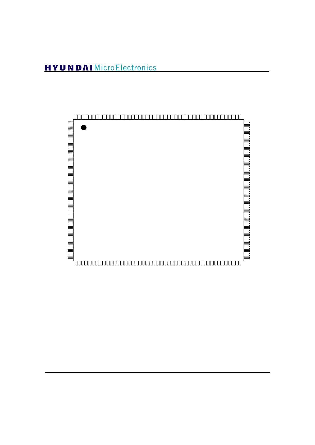
3. Pin Description
60
HME
SDRAM_DATA[38]
VDD
SDRAM_DATA[37]
SDRAM_DATA[36]
P_SHARE_
P_SHARE_
P_SHARE_
MCLK_OUT
TEST_ OUT[2]
FP_FD
MCLK_IN
DEC_ERROR
VSS
P_WAIT
PIC_DIS_SYNC
VDD
VDD
PDATA[31]
PDATA[30]
PDATA[29]
PDATA[28]
VSS
VSS
PDATA[27]
PDATA[26]
PDATA[25]
PDATA[24]
VDD
PDATA[23]
PDATA[22]
PDATA[21]
PDATA[20]
VSS
PDATA[19]
PDATA[18]
VDD
PDATA[17]
PDATA[16]
PDATA[15]
VDD
PDATA[14]
PDATA[13]
PDATA[12]
VSS
PDATA[11]
VSS
PDATA[10]
VDD
PDATA[9]
PDATA[8]
VDD
PDATA[7]
PDATA[6]
PDATA[5]
PDATA[4]
VSS
VSS
PDATA[3]
VDD
VDD
PDATA[2]
PDATA[1]
PDATA[0]
VSS
5101520253035
40
45
50
55
65
7075808590
95
100
105
110
115
120
190
185
195
200
205
210
215
220
225
230
235
IN[10]
IN[9]
IN[8]
240
VSS
VDD
VSS
\RESET
TSW
\VIDEN
VSTCW
VSS
VDD
VSS
VDD
VSS
SCL
VSS
SDA
\INT_V
VDD
VSS
VDD
VDD
VDD
VSS
VDD
VSS
VDD
VSS
1
VSS
SDRAM_DATA[20]
VDD
SDRAM_DATA[19]
VSS
SCANTESTON
IDCTTESTON
MEMTESTON
CLK_27M
VID_STRB
VID_DATA[0]
VID_DATA[1]
VID_DATA[2]
VID_DATA[3]
VID_DATA[4]
VID_DATA[5]
VID_DATA[6]
VID_DATA[7]
\VID_REQ
\UBUFF_FULL
SDRAM_DATA[0]
SDRAM_DATA[1]
SDRAM_DATA[2]
SDRAM_DATA[3]
SDRAM_DATA[4]
SDRAM_DATA[5]
SDRAM_DATA[6]
SDRAM_DATA[7]
SDRAM_DATA[8]
SDRAM_DATA[9]
SDRAM_DATA[10]
SDRAM_DATA[11]
SDRAM_DATA[12]
SDRAM_DATA[13]
SDRAM_DATA[14]
SDRAM_DATA[15]
SDRAM_DATA[16]
SDRAM_DATA[17]
SDRAM_DATA[18]
VDD
SDRAM_DATA[21]
VSS
SDRAM_DATA[22]
VDD
SDRAM_DATA[23]
SDRAM_DATA[25]
SDRAM_DATA[24]
GDC21D401B
YYWWA
VSS
MCLK
VDD
SDRAM_ADDR[6]
SDRAM_ADDR[1]
VDD
SDRAM_ADDR[5]
VDD
SDRAM_ADDR[2]
SDRAM_ADDR[4]
VSS
SDRAM_ADDR[3]
VSS
SDRAM_DATA[31]
SDRAM_DATA[30]
VDD
SDRAM_DATA[29]
SDRAM_DATA[28]
VSS
SDRAM_DATA[27]
SDRAM_DATA[26]
VDD
GDC21D401B
VSS
180
PSTR[1]
PSTR[0]
PDWIN
VSS
175
D_INFO_WIN
DIS_INFO
VDD
VDD
\FFPN
170
VSS
MBFI
MBCLK
VDD
SCLK
165
VDCLK
VSS
SDRAM_DATA[63]
SDRAM_DATA[62]
SDRAM_DATA[61]
160
VDD
VDD
SDRAM_DATA[60]
SDRAM_DATA[59]
VSS
155
VSS
SDRAM_DATA[58]
VDD
SDRAM_DATA[57]
VSS
150
SDRAM_DATA[56]
VDD
SDRAM_DATA[55]
SDRAM_DATA[54]
VSS
145
SDRAM_DATA[53]
SDRAM_DATA[52]
VDD
SDRAM_DATA[51]
SDRAM_DATA[50]
140
VSS
SDRAM_DATA[49]
SDRAM_DATA[48]
VDD
SDRAM_DATA[47]
135
VDD
SDRAM_DATA[46]
SDRAM_DATA[45]
VSS
VSS
130
SDRAM_DATA[44]
VDD
SDRAM_DATA[43]
VDD
SDRAM_DATA[42]
125
SDRAM_DATA[41]
VSS
SDRAM_DATA[40]
VSS
SDRAM_DATA[39]
SDRAM_DATA[35]
VSS
SDRAM_DATA[34]
SDRAM_DATA[33]
SDRAM_DATA[32]
VDD
VDD
CSN
RASN
CASN
WEN
VSS
BA0
SDRAM_ADDR[10]
SDRAM_ADDR[9]
SDRAM_ADDR[8]
VDD
SDRAM_ADDR[7]
SDRAM_ADDR[0]
VSS
VSS
6
Figure 1. Pin Description
Page 6
(Package: 240 HQFP)
NAME PIN TYPE DESCRIPTION
VDCLK
MCLK
MCLK_IN
MCLK_OUT
CLK_27M
\RESET
SCL
SDA
VID_DATA[7:0]
\VID_REQ
VID_STRB
TSW
\VIDEN
VSTCW
\INT_V
\UBUFF_FULL
CSN
WEN
RASN
CASN
BA0
SDRAM_ADDR
[10:0]
SDRAM_DATA
[63:0]
25,23,21,20,
CLOCK
165 I
94 I
234
237
6 I
O
Operating clock. - 54 MHz (max), 50 % duty cycle
SDRAM interface clock. - 81 MHz (max), 50 % duty cycle
SDRAM interface clock. - 81 MHz (max),
I
50 % duty cycle (the same clock as MCLK)
SDRAM interface clock through clock buffer for delay effect.
This signal input is MCLK_IN.
External system time clock. - 27 MHz
RESET
8 I Power on reset(active low). At least 3 VDCLKs.
Decoding starts after 128 VDCLKs from the last reset low state.
I2C-BUS INTERFACE
26 I
28 I/O
I2C-bus serial clock. - 400 KHz(max)
I2C-bus serial data
TRANSPORT INTERFACE
I
Transport Decoder data bus
18,16,15,14
29 O
13 I
Transport data request(active low)
Transport data strobe.
VID_DATA[7:0] is latched on the rising edge.
9 I
PTS & DTS data enable(active high).
In LG DTV chipset, this signal is connected to the
PTS_DTS_STRB pin of GDC21D301A.
10 I
11 I
Video bitstream data enable(active low)
STC data enable(active high)
HOST INTERRUPT
31 O
30 O
Video decoder interrupt(active low)
User data FIFO is full(active low).
When it happens, host microprocessor must read the user data
from user data FIFO.
Otherwise video decoder suspends decoding.
SDRAM INTERFACE
109 O
106 O
108 O
107 O
104 O
SDRAM chip selection(active low)
SDRAM write enable(active low)
SDRAM row address selection(active low)
SDRAM column address selection(active low)
SDRAM bank address.
This indicates bank address, and low value selects bank ‘0’ .
103,102,101,
99,92,89,86,
84,87,91,98
163,162,161,
158,157,154,
152,150,43,
42,40,39,38,
36, 34, 33
O
I/O
SDRAM address
SDRAM data bus
GDC21D401B
7
Page 7
Pin Description (continued)
NAME PIN TYPE DESCRIPTION
VDP INTERFACE - SYNC & PICTURE FORMAT
DIS_INFO
D_INFO_WIN
PIC_DIS_SYNC
P_WAIT
PDWIN
PSTR[1:0]
\FFPN
SCLK
MBCLK
DEC_ERROR
FP_FD
174 O
175 O
230 I
231 I
177 O
179,178 O
171 O
166 O
168 O
233 O
235 O
GDC21D401B
Serialized picture format data
Serialized picture format data enable(active high)
Picture display sync. - 30 Hz or 29.97 Hz, 50% duty
VDP INTERFACE – PICTURE DATA
PDATA wait(active high).
This signal makes PDATA output to be suspended after 50
VDCLKs from the last high value.
This signal is the output of the VDP.
Picture data window(active high).
During 1 picture data decoding, this signal is high.
Picture structure.
This indicates the structure of output picture.
If this is equal to ‘1’ , the output picture is top field picture.
If this is equal to ‘2’ , the output picture is bottom field
picture.
If this is equal to ‘3’ , the output picture is frame picture.
First field parity(active low).
This signal is the first_field_parity flag of output picture.
When output picture is interlaced frame picture, the field of
output frame is the first output by the VDP.
Slice decoding window(active high).
This signal has high value when a macroblock with the same
vertical position is decoded. There are at least 2-clock low
value periods between each slice decoding window.
Macroblock decoding window(active high).
This signal has high value when a macroblock data is
decoded. The width of high value is always 96 VDCLKs.
There are at least 2-clock low value periods between each
macroblock decoding window.
Decoding Error (active high)
This is a multiplexed output signal.
It is used to inform VDP R1.2 (GDC21D701B) of an error in
Picture or Macro Block.
Frame_Pred_Frame_Dct (active high)
This signal is explained in ISO/IEC 13818-2
(Information technology – Generic coding of moving
pictures and associated audio information : Video)
If this flag is set to ‘1’ , only frame_DCT and frame prediction
are used. In a field picture, it should be ‘0’ .
If progressive_frame is ‘1’ , Frame_pred_frame_dct should be
set to ‘1’ . This flag affects the syntax of the bitstream.
8
Page 8
Pin Description (continued)
227,226,225,
224,221,220,
191,190,187,
NAME PIN TYPE DESCRIPTION
MBFI
PDATA[31:0]
169 O
184,183,182
GDC21D401B
Macroblock Field IDCT.
This signal has the meaning when a decoded picture is a frame
picture. If this is set to ‘0’ , the output of a decoded
macroblock has the form of frame IDCT.
If this is set to ‘1’ , the output of a decoded macroblock has the
form of field IDCT.
O
Picture data.
This is a bundle of four adjacent pixel data.
A decoded macroblock consists of 96 consequent PDATA.
The order of PDATA in a decoded macroblock depends on the
MBFI signal.
9
Page 9
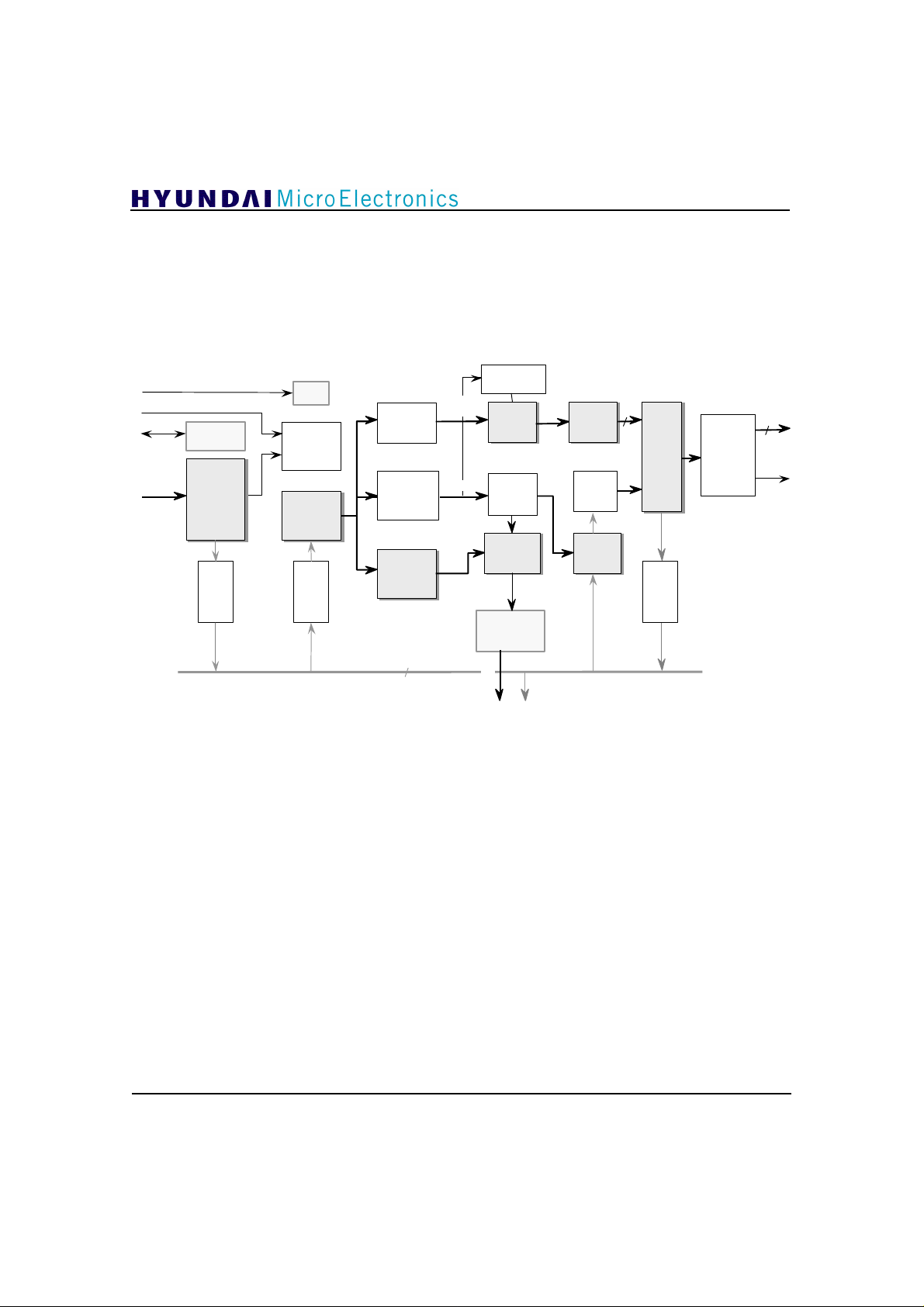
4. Block Diagram
GDC21D401B
MHz System Clock
27
Display Sync
Video
Bitstream
I C I/F
2
Video
Bitstream
Predecoder
FIFO
STC
DTS check
Decoding
Controller
Sequence
Parcer
FIFO
IDCT
Coefficient
Decoder
Macroblock
Parameter
Decoder
Motion
Vector
Decoder
64
Internal Data Bus
IDCT
coefficients
MB
parameters
MB
Motion
Vector
Quantization
Matrix
IQ
IQ
&
&
Buffer
Buffer
MB
Decoding
Controller
MV
Processor
SDRAM
Controller
Address
Data
Max. M sample/sec
200
High-Speed IDCT
32
IDCT
IDCT
FIFO
Half-pel
Predictor
Predictor
FIFO
Display
Processor
Control
Decoded
MB Data
32
Data
Window
10
Figure 2. MPEG-2 MP@HL Video Decoder Block Diagram
Page 10

5. Functional Description
5.1 Initialization and Decoding Start
GDC21D401B
5.2 Picture Decoding
¥¡) Power on reset: \RESET = ‘0’ during several
clocks. In this state, bitstream buffers are flushed,
all decoding controllers are reset, and all internal
registers have default values.
¥¢) Decoding start: \RESET = ‘1’ . In this state,
the bitstream buffers begin to be filled with input
video bitstreams. First, the bitstream is discarded
until the 1st sequence header code appears, and
then the sequence headers are decoded. Next, the
picture data bitstream is decoded, and it continues
to be decoded unless the buffers are underflow.
WAIT
SYNC
Picture decoding control state diagram is shown in
Fig 3. Each picture decoding is synchronized with
the external ‘pic_dis_sync‘ signal. If
‘pic_dis_sync‘ signal is changed, command is
executed, then some decoding conditions are
checked (sync parity: top or bottom, underflow,
DTS check and skip check). If the condition is
“repeat”, decoding is suspended until this
condition is ended. If the condition is “skip”, one
picture frame data is skipped. Or else decoding
sync is generated, and controller is suspended for
given ‘pic_dis_sync‘ duration which is
determined by picture format information. If
picture decoding is completed within the given
‘pic_dis_sync’ duration, the state is changed to
wait sync state, and next decoding cycle is
executed. If picture decoding is not completed
within the given duration, the state is changed to
task overrun state. In the task overrun state, as
soon as picture decoding is completed, next
decoding cycle is executed without waiting
‘pic_dis_sync’ transition.
PIC_DIS_SYNC =
or
DEC. COMPLETE
WAIT
PIC_DIS_SYNC = or
Figure 3. Picture Decoding Control State Diagram
DEC. COMPLETE
TASK
OVERRUN
DEC.
SYNC
GEN.
COMMAND
DEC.
CHECK
SKIP
SKIP
WAIT
REPEAT
11
Page 11

5.3 STC (System Time Clock)
Generation
Internal STC counter is supported. STC value
should be loaded after the reset by host
microprocessor or transport decoder, and be
counted at 90 KHz clock derived from external 27
MHz system clock. Also it should be loaded
whenever the system time base is changed. 27
MHz system clock is supplied by transport
decoder through external 27 MHz clock input.
5.4 DTS (Decoding Time Stamp)
Synchronization
The DTS values are determined when the
associated pictures are decoded referring to the
STC. The transport decoder must extract PTS &
DTS values from MPEG-2 system layer, and
transfer them to the VD through host interface or
transport data interface. DTS values are extracted
and stored in DTS-FIFO with 8-bit associated
picture numbers(they are defined by the VD
internally).
Before each picture decoding, picture decoding
controller checks if there is a DTS associated with
each picture. And it compares the DTS value from
DTS-FIFO with STC value.
The DTS value is considered to match the current
STC value if the DTS satisfies this equation:
STC + jitter_b(negative) < DTS < STC + jitter_f(positive)
In the case that jitter is the tolerance for the
comparison:
If the DTS is less than STC + jitter_b (in
other words, the time for current picture
decoding has already passed), picture
decoding controller discards B picture in
VBV delay mode and any picture in low
delay mode without decoding it.
If the DTS is greater than STC + jitter_f (the
time for current picture decoding has not
come yet), picture decoding controller pauses
decoding process until the DTS value falls
within the allowed tolerance of STC.
GDC21D401B
When system time base is changed, the time base
of the current DTS can differ from that of the new
STC temporarily because of video decoding delay.
In this case, for about 0.5 sec, DTS
synchronization mode must be disabled by using
decoding mode register.
5.5 Error Concealment
When the VLD detects a bitstream syntax error or
an MPEG-2 error code (0x000001B4), it performs
appropriate error handling and error concealment
to continue the decoding and to minimize the
effect of the error on decoded video. If an error
occurs at picture data layer, the slice-based error
concealment is performed. If an error occurs at
header layer, the associated sequence is skipped.
5.6 User Data Read
User data in MPEG Video Sequence can be read
through host interface(I2C) as follows. If user data
interrupt is enabled, user data is stored in internal
user data FIFO, and once ‘PIC_DEC_SYNC’ is
set to ‘high’ , a interrupt signal is generated which
informs host that user data is stored in user data
FIFO. If user data interrupt is disabled, user data
is discarded.
When user data interrupt signal is generated, host
reads the ‘U_D_COUNT’ register for bytes of
user data FIFO. And then it reads the
‘USER_DATA’ register(user data FIFO output)
repeatedly as many as the number of
‘U_D_COUNT’ register. In this case, the host
had better use I2C burst read cycle for reading
speed efficiency.
If internal user data FIFO becomes full during user
data interrupts, ‘\UBUFF_FULL’ signal is
generated. And also the host reads user data by
using the same method as that of user data
interrupt.
12
Page 12

GDC21D401B
5.7 Bitstream Buffer Over/Underflow
The bitsream buffer should not be overflowed or
underflowed in proper operation. When bitstream
buffer is overflowed, video bitstream input is
disabled during overflow. At the beginning of each
picture, buffer underflow is checked. If the
bitstream buffer doesn’t include 1 picture
bitstream, decoding is paused until this buffer is
filled with 1 picture bitstream.
5.8 VLD (Variable Length Decoder)
The VLD executes the variable length decoding of
MPEG-2 MP@HL. It is composed of sequence
syntax parsing and code decoding. Headers, IDCT
coefficients, and motion vectors are generated from
input video bitstream by the VLD.
5.9 Inverse Quantization
For decoding a macroblock, various parameters
are transmitted to IQ block and MC block in
sequence of decoding syntax from the VLD.
Coefficient data transmitted to IQ block is
multiplied by quantization matrix and quantization
scale. Quantized coefficients are stored in two
coefficient buffers, and if a request from MC block
occurs, the buffer outputs 4 coefficients in parallel.
Inverse scan processing is performed in the
coefficient buffer by varying read/write address
according to scan type.
5.10 IDCT (Inverse Discrete Cosine
Transform)
Coefficient data from IQ block is transmitted to
IDCT block. IDCT block transforms these
coefficients to pixel data or differential pixel data
which have the values in the range of -256 to 255.
For one 8x8 DCT block, the elapse time through
IDCT block is a 30-VDCLK period. In the IDCT
block, 8 adjacent coefficients are processed in
parallel. The maximum transform speed of the
IDCT block is 1 VDCLK x 4 Sample/sec. This
speed is sufficient for decoding 1920x1088 30Hz
frame data.
5.11 MC(Motion Compensation)
Motion Compensation Block restores macroblocks
by using macroblock difference data from IDCT
block and reference data which are read from
external SDRAM. Address Generation Block in
the MC generates SDRAM address by
transforming macroblock address and motion
vector to row/column address of SDRAM. The
MC block supports all motion types of frames and
field pictures. Motion vector range decoded in the
MC has the range of f_code=9 for horizontal
motion vector and f_code=8 for vertical motion
vector. Reconstructed macroblock in the MC block
is stored in the external frame memory for I or P
picture, but in the case of B picture, decoded
macroblock is transmitted directly to the VDP
without being stored in the frame memory.
Because reordering occurs in I or P picture
decoding, macroblock data to be displayed is read
from reference frame memory and is transmitted to
the VDP in the form of macroblock.
13
Page 13

5.12 Transport Interface
GDC21D401B
8-bit parallel data(vid_data[7:0]) interface is
supported for transport data interface. Three kinds
of data (Video bitstream, STC, and DTS) can be
transferred through transport data interface.
If \vid_en is low, video bitstream is transferred. If
vstcw is high, STC is transferred. If tsw is high,
PTS & DTS are transferred. Or else no data is
VID_STRB
TSW
VSTCW
\VID_EN
VID_DATA
VID_STRB
TSW
32
23:1631:24
PTS[32:0]
15:8
7:0
32
all ‘ 0’
all ‘ 1’
23:1631:24
DTS[32:0]
all ‘ 0’
transferred.
Vid_data[7:0] is latched on the rising edge of
vid_strb. When \VID_REQ is high, transport
data interface is disabled, and when \VID_REQ is
low, transport data interface is enabled. See the
following Fig. 4.
15:8
7:0
32
23:1631:24
PTS[32:0]
15:8
7:0
14
VSTCW
\VID_EN
VID_DATA
32
23:1631:24
STC[32:0]
15:8
7:0
. . . . .
Video Bitstream
Figure 4. Transport Data Interface Timing Diagram
Page 14

5.13 Host Interface
GDC21D401B
I2C bus interface
I2C bus interface is used for host data interface. It
operates only as a Slave. The Chip-ID(dev
address) of this IC is “0001111”b. Data on the
I2C-bus can be transferred at the rate up to 100
START
CHIP ID
0001111
S 0
START
CHIP ID
0001111
S 0
WRITE
ACK
0 REG. ADDR.(7:0) 0 S 0001111 0 REG. DATA(7:0)0 0 P
ACK ACK
Figure 5. Write Cycle Diagram
WRITE
ACK
0 REG. ADDR.(7:0) 0 S 0001111 0 REG. DATA(7:0)1 1 P
ACK ACK
START
START
kbit/s in the standard mode, or up to 400 kbit/s in
the fast mode. I2C bus data read/write formats of
this IC are shown in the Fig 5, 6, and 7. Burst
Read Cycle can be used for the user data reading.
For more information, see the I2C bus interface
standard.
PAUSE
PAUSE
CHIP ID
CHIP ID
WRITE
ACK
READ
ACK
START
CHIP ID
0001111
S 0
Figure 6. Read Cycle Diagram
WRITE
ACK
0 REG. ADDR.(7:0) 0 S 0001111 0 REG. DATA(7:0)1 0
START
ACK ACK
CHIP ID
ACK ACK
READ
ACK
REG. DATA(7:0) 1 PREG. DATA(7:0) 0 . . . . . .
Figure 7. Burst Read Cycle Diagram
PAUSE
15
Page 15

GDC21D401B
Interrupt Mechanism
The host enables specific interrupt events to occur
by setting the mask value of internal interrupt.
When an event occurs and corresponding interrupt
enable is set, an interrupt bit is set in an interrupt
register. Everytime each picture decodes sync, host
checks the contents of that register, and if any bit
Table 2. Bit Definitions for Interrupt Register & Mask
BIT # MNEMONIC EVENT EVENT DEFINITION
0 PIC_S Picture decoding New picture is decoded.
1 GOP_H GOP header decoding GOP headers are decoded.
2 SEQ_H Seq. header decoding Sequence headers are decoded.
3 SEQ_E Seq. end decoding Sequence end code is decoded.
4 USR User data ready
User data has been extracted and stored in the buffer. When
the interrupt is disabled, user data is discarded.
5 OVF Buffer overflow Bitstream buffer is full.
6 UND/PTS Buffer underflow/
PTS received
Dec_mode(4) = ‘0’ :
Bitstream buffer doesn’t have 1 picture bitstream.
Dec_mode(4) = ‘1’
PTS value is received through transport interface.
7 ERR Bitstream error Error code or syntax error is detected in the bitstream
(header layer).
is set, it generates an interrupt. Exceptionally, in
the case of OVF, UND and ERR interrupt signals
are generated as soon as the error is detected.
When the host serves the interrupt, interrupt
register and interrupt signal are reset.
16
Page 16

GDC21D401B
Register Description
Table 3. Internal Register Description
NO NAME SIZE DESCRIPTION DEFAULT R/W
0 Command 3 High level decoding command. play() R/W
1 Interrupt 8 Interrupt register. all ‘0’ R
2 DTS0 8 DTS[7:0]. When it is written by host
microprocessor, DTS[19:0] values are stored in the
DTS-FIFO.
When DTS value is received through transport
interface, it can be read via the DTS registers
3 DTS1 8 DTS[15:8]. all ‘0’ R/W
4 DTS2 4 DTS[19:16]. all ‘0’ R/W
5 Jitter_f0 8 Forward tolerance of DTS synchronization,
Jitter_f[7:0]. When it is written by host
microprocessor, Jitter_f[19:16] values are applied.
6 Jitter_f1 8 Jitter_f[15:8]. h”0E” R/W
7 Jitter_f2 4 Jitter_f[19:16]. h“0” R/W
8 Jitter_b0 8 Backward tolerance of DTS synchronization,
Jitter_b[7:0]. When it is written by host
microprocessor, Jitter_b[19:16] values are applied.
9 Jitter_b1 8 Jitter_b[15:8]. h“FA” R/W
10 Jitter_b2 4 Jitter_b[19:16]. h“F” R/W
11 Slm_num 6 Slow motion command of repeated numbers. h’8’ R/W
12 Header 8 Header data register. It has header value indicated
by H_addr.
13 H_addr 8 Header data address. all ‘0’ R/W
14 User_data 8 User data register. It is an output of the User data
FIFO.
15 U_d_count 7 User data count in the User data FIFO. all ‘0’ R
16 Int_mask 8 Interrupt mask. all ‘0’ R/W
17 Dec_mode 8 Decoding mode. all ‘0’ R/W
18 STC0 8 System time clock, STC[7:0]. When it is written by
host microprocessor, STC[19:0] values are loaded
to internal STC counter.
19 STC1 8 STC[15:8]. all ‘0’ R/W
20 STC2 4 STC[19:16]. all ‘0’ R/W
21 W_ptr 8 Write address pointer of the bitstream buffer. Unit
value is 65,536 bits.
22 R_ptr 8 Read address pointer of the bitstream buffer. Unit
value is 65,536 bits.
23 PTS0 8 PTS[7:0]. When PTS value is received through
tranport interface, it is stored in the PTS registers.
24 PTS1 8 PTS[15:8]. all ‘ 0’ R
25 PTS2 4 PTS[19:16]. all ‘0’ R
all ‘0’ R/W
h”10” R/W
h“BA” R/W
all ‘0’ R
all ‘0’ R
all ‘0’ R/W
all ‘0’ R
all ‘0’ R
all ‘0’ R
17
Page 17

Table 4. Definitions of Command Register.
REG. VALUE COMMAND DESCRIPTION
0 Reset() Bitstream buffer is flushed and decoding controllers are reset.
1 Play() Start normal bitstream decoding.
2 Slow_motion()
3 Scan() Skip to I picture and continue decoding.
4 Single_step() Decode 1 picture and pause.
5 Pause() Decoding pause.
6 Fast_forward() Decode only I or P picture.
7 NoCOM() No command is loaded in the register. In this state bitstream buffer
Decode pictures and pause during slm_num duration, and repeat this
process.
continues to be filled with input bitstreams.
Table 5. Definition of Header Address
H_ADDR HEADER
0 H_size[7:0]
1 V_size[7:0]
2 ‘0’ & h_size[10;8] & ‘ 0’ & v_size[10:8]
3 Aspect_ratio[3:0] & frame_rate[3:0]
4 ‘0’ &prog_seq&’ 0’ &low_delay& pict_cod_type[1:0]& ‘0’ &repeat_first_field
5 Matrix_coefficients[7:0]
6 VBV_delay[7:0]
7 VBV_delay[15:8]
8 Time_code[7:0]
9 Time_code[15:8]
10 Time_code[23:16]
11 “0000000”&Time_code[24]
12 Temporal_reference[7:0]
13 “000000”&Temporal reference[8:9]
14 Copyright_extension[7:0]
15 Copyright_extension[15:8]
16 Copyright_extension[23:16]
17 Copyright_extension[31:24]
18 Copyright_extension[39:32]
19 Copyright_extension[47:40]
20 Copyright_extension[55:48]
21 Copyright_extension[63:56]
22 Copyright_extension[71:64]
23 Copyright_extension[79:72]
24 “0000”&Copyright_extension[83:80]
GDC21D401B
18
Page 18

Table 6. Definition of Decoding Mode Register
BIT # DESCRIPTION
0 It must have “High”.
1 DTS input timing: ‘0’ => DTS values are transferred to VD before the associated PSTC.
‘1’ => DTS values are transferred to VD after the associated PSTC.
PSTC represents the Picture Start Code.
2 DTS synchronization: ‘0’ => disabled ‘ 1’ => enabled
3 Picture reordering in VBV delay mode: ‘0’ => enabled ‘ 1’ => disabled
4 Int_reg(6) & Int_mask(6) selection: ‘0’ => UND ‘ 1’ => PTS
5~7 “000” : Not used
GDC21D401B
19
Page 19

5.14 Video Data Output Format
21918
3
016171623227420215271026
11
258249311430
15
291228133451503532484933385554
39
36525337425958
43
4056574146636247446061456667646570716869747572737879767782838081868784859091888994959293219183016171623227420215271026112582493114301529122813345150353248493338555439365253374259584340565741466362474460614566676465707168697475727378797677828380818687848590918889949592
93
GDC21D401B
Video decoder transmits decoded macroblock data
to the VDP via 32-bit bus. This bus consists of 4
adjacent pixel components. For a macroblock data,
the number of 32-bit data is 96. The order of
output data is the same of decoded block in the
MPEG-2 Video bitstream syntax. For this reason,
output sequence depends on the DCT_TYPE of
decoded macroblock. Except for the macroblock
whose parameter is Frame picture and Field DCT,
all macroblock outputs have the sequence of below
figure(MBFI=0) in Fig 8. The top field data of the
macroblock whose DCT_TYPE is field
type(MBFI=1) is transmitted before the
macroblock bottom field data for the luminance
data. But the chrominance data has always the
same sequence.
MBFI == 0
MBFI == 1
Figure 8. The Sequence of Macroblock Output
20
Page 20

5.15 Video Data Output Timing
GDC21D401B
During decoding the picture which is field picture
or frame picture, PDWIN signal is high. Between
each picture decoding time, there is low level
period of PDWIN signal, and it is longer than 128
VDCLKs. Picture parameter such as PSTR[1:0] or
\FFPN is determined 2 clocks before PDWIN
PDWIN
PSTR[1:0]
\FFPN
SCLK
2 VDCLKs Minimum
SCLK
MBCLK
MBFI
1 VDCLK
rising edge. Its value is not changed until PDWIN
falling edge. SCLK shows that new slice decoding
is started on its rising edge. Width of MBCLK
high pulse is always 96 clocks, and low value
period is longer than 2 clocks.
Minimum
128 VDCLKs
PDATA[31:0]
VDCLK
0 1 2 3 9594
Figure 9. Timing Diagram
21
Page 21

5.16 SDRAM Interface
GDC21D401B
For storing reference frame data and bitstream,
very large external memory is required. For this
reason, 64-Mbit external memory
(GM72V161621AT or same type of memory) is
needed. The memory configuration is shown in the
following Fig 10. Four 16-Mbit memories are
directly attached to the VD. Data bus for
Revision Note for SDRAM Clock Application Note(1):
Recommended
CSN,WEN,RASN,CASN, BA0
SDRAM_ADDR[10:0]
SDRAM_DATA[63:0]
MCLK
# 94
4 ~ 10.5ns
5
11
64
SDRAMs is configured to 64-bit bus. Memory
interface clock should be supplied to the VD and
four SDRAMs with same clock phase. Higher
frequency for MCLK and higher decoding speed
can be achieved. The maximum frequency of
MCLK is 81 MHz. This clock doesn’t need to be
locked with any other input clock.
16
SDRAM
CLK
SDRAM
16
CLK
22
CLK
Driver
MCLK_IN
MCLK_OUT
VSS
N.C.
(No Connect)
Figure 10. External Memory Interface 1
16
16
SDRAM
CLK
SDRAM
CLK
Page 22

Revision Note for SDRAM Clock Application Note(2)
GDC21D401B
CSN,WEN,RASN,CASN, BA0
SDRAM_ADDR[10:0]
SDRAM_DATA[63:0]
MCLK
MCLK_IN
MCLK_OUT
CLK
Driver
# 94
# 234
# 237
5
11
64
# 234 # 237
Clock delay equivalent circuit
16
16
16
16
2 ~ 5 ns
SDRAM
CLK
SDRAM
CLK
SDRAM
CLK
SDRAM
CLK
Figure 11. External Memory Interface 2
23
Page 23

GDC21D401B
6. Electrical Specification
6.1 Absolute Maximum Rating
SYMBOL PARAMETERS VALUES UNIT
V
DD
V
I
Vo
T
stg
P
d
*Note :Absolute Maximum Ratings mean that the safety of the device cannot be guaranteed beyond these values,
and this doesn’t imply that the device should be operated within these limits.
6.2 Recommended Operating Range
SYMBOL PARAMETERS VALUES UNIT
V
DD
T
opr
6.3 DC Characteristics (VDD = 3.3 V¡¾10%, TA = 0 ~ 70¡É)
Power Supply Voltage -0.33 to 5.5 V
Digital Input Voltage -0.33 to VDD + 0.5 V
Digital Output Voltage -0.33 to VDD + 0.5 V
Storage Temperature -55 to 125
°C
Power Dissipation 4.6 W
Power Supply Voltage
Operating Temperature 0 to 70
3.3 ± 10%
°C
V
SYMBOL PARAMETER MIN MAX UNIT
V
V
V
V
I
I
F
IH
IL
OH
OL
DD
DDQ
OPR
Input High Voltage 0.7X V
Input Low Voltage -0.33 0.2X V
Output High Voltage 2.4 V
Output Low Voltage 0 0.4 V
Operating Current - 900 mA
Standby Current - 10 uA
Operating Frequency - 54 MHz
DD
V
+0.33 V
DD
DD
DD
V
V
24
Page 24

6.4 AC Characteristics (VDD = 3.3 V¡¾10%, TA = 0 ~ 70¡É)
All Outputs
All Intputs
CHclk27m/tCLvdclk
CHvid strb/tCLvdclk
t
CP
MCLK
VDCLK
CLK27M
VID_STRB
t
CH
t
CL
GDC21D401B
except for
SDRAM I/F
signals
except for
SRAM I/F
signals
t
S
t
OD
t
H
Figure 12. Input/Output Timing
SYMBOL PARAMETERS MIN MAX TYPE UNIT
t
CPmclk
t
CPvdclk
t
CPclk27m
t
CPvid strb
t
CHmclk/tCLmclk
t
CHvdclk/tCLvdclk
t
t
t
H
ts
t
OD
Clock Period - - 13 ns
Clock Period - - 20 ns
Clock Period - - 36 ns
Clock Period - - 36 ns
Clock High Time/Clock Low Time 5.5 7.5 - ns
Clock High Time/Clock Low Time 8 12 - ns
Clock High Time/Clock Low Time 16 20 - ns
Clock High Time/Clock Low Time 16 20 - ns
Input Hold Time 7 - - ns
Input Setup Time 7 - - ns
Output Delay Time - 17 - ns
*Note : Low voltage input signal rising and falling edge switching time = 1.0 ns
SDRAM I/F AC Characteristics (GDC21D401HQ)
SIGNAL SYMBOL MIN MAX TYPE UNIT
SDRAM_DATA[63:0]
SDRAM_ADDR[10:0] Propagation Delay 4 10.5 - ns
BA0 Propagation Delay 4 10.5 - ns
CSN, WEN, RASN,
CASN
*Test Condition : Load Capacitance = 20pF
1.Min. Condition : Temperature = 0 °C, VDD = 3.6 V
2. Max. Condition : Temperature = 100 °C, VDD = 3.0 V
Propagation Delay 4 10.5 - ns
Setup Time 0 0 - ns
Hold Time 2 3 - ns
Propagation Delay 4 10.5 - ns
25
Page 25

7. Package Mechanical Data
7.1 Package Pin Out
PIN TYPE NAME PIN TYPE NAME
1 GND VSS 41 PWR VDD
2 I SCANTESTON 42 I/O SDRAM_DATA[6]
3 PWR VDD 43 I/O SDRAM_DATA[7]
4 I IDCTTESTON 44 PWR VDD
5 I MEMTESTON 45 I/O SDRAM_DATA[8]
6 I CLK_27M 46 GND VSS
7 GND VSS 47 I/O SDRAM_DATA[9]
8 I \RESET 48 I/O SDRAM_DATA[10]
9 I TSW 49 PWR VDD
10 I \VIDEN 50 I/O SDRAM_DATA[11]
11 I VSTCW 51 I/O SDRAM_DATA[12]
12 GND VSS 52 GND VSS
13 I VID_STRB 53 I/O SDRAM_DATA[13]
14 I VID_DATA[0] 54 I/O SDRAM_DATA[14]
15 I VID_DATA[1] 55 PWR VDD
16 I VID_DATA[2] 56 I/O SDRAM_DATA[15]
17 PWR VDD 57 I/O SDRAM_DATA[16]
18 I VID_DATA[3] 58 GND VSS
19 GND VSS 59 I/O SDRAM_DATA[17]
20 I VID_DATA[4] 60 I/O SDRAM_DATA[18]
21 I VID_DATA[5] 61 GND VSS
22 PWR VDD 62 I/O SDRAM_DATA[19]
23 I VID_DATA[6] 63 PWR VDD
24 GND VSS 64 I/O SDRAM_DATA[20]
25 I VID_DATA[7] 65 GND VSS
26 I SCL 66 I/O SDRAM_DATA[21]
27 GND VSS 67 PWR VDD
28 I/O SDA 68 I/O SDRAM_DATA[22]
29 O \VID_REQ 69 GND VSS
30 O \UBUFF_FULL 70 I/O SDRAM_DATA[23]
31 O \INT_V 71 PWR VDD
32 PWR VDD 72 I/O SDRAM_DATA[24]
33 I/O SDRAM_DATA[0] 73 I/O SDRAM_DATA[25]
34 I/O SDRAM_DATA[1] 74 PWR VDD
35 GND VSS 75 I/O SDRAM_DATA[26]
36 I/O SDRAM_DATA[2] 76 I/O SDRAM_DATA[27]
37 PWR VDD 77 GND VSS
38 I/O SDRAM_DATA[3] 78 I/O SDRAM_DATA[28]
39 I/O SDRAM_DATA[4] 79 I/O SDRAM_DATA[29]
40 I/O SDRAM_DATA[5] 80 PWR VDD
GDC21D401B
26
Page 26

Package Pin Out(continued)
PIN TYPE NAME PIN TYPE NAME
81 I/O SDRAM_DATA[30] 124 GND VSS
82 I/O SDRAM_DATA[31] 125 I/O SDRAM_DATA[41]
83 GND VSS 126 I/O SDRAM_DATA[42]
84 O SDRAM_ADDR[3] 127 PWR VDD
85 GND VSS 128 I/O SDRAM_DATA[43]
86 O SDRAM_ADDR[4] 129 PWR VDD
87 O SDRAM_ADDR[2] 130 I/O SDRAM_DATA[44]
88 PWR VDD 131 GND VSS
89 O SDRAM_ADDR[5] 132 GND VSS
90 PWR VDD 133 I/O SDRAM_DATA[45]
91 O SDRAM_ADDR[1] 134 I/O SDRAM_DATA[46]
92 O SDRAM_ADDR[6] 135 PWR VDD
93 PWR VDD 136 I/O SDRAM_DATA[47]
94 I MCLK 137 PWR VDD
95 GND VSS 138 I/O SDRAM_DATA[48]
96 GND VSS 139 I/O SDRAM_DATA[49]
97 GND VSS 140 GND VSS
98 O SDRAM_ADDR[0] 141 I/O SDRAM_DATA[50]
99 O SDRAM_ADDR[7] 142 I/O SDRAM_DATA[51]
100 PWR VDD 143 PWR VDD
101 O SDRAM_ADDR[8] 144 I/O SDRAM_DATA[52]
102 O SDRAM_ADDR[9] 145 I/O SDRAM_DATA[53]
103 O SDRAM_ADDR[10] 146 GND VSS
104 O BA0 147 I/O SDRAM_DATA[54]
105 GND VSS 148 I/O SDRAM_DATA[55]
106 O WEN 149 PWR VDD
107 O CASN 150 I/O SDRAM_DATA[56]
108 O RASN 151 GND VSS
109 O CSN 152 I/O SDRAM_DATA[57]
110 PWR VDD 153 PWR VDD
111 PWR VDD 154 I/O SDRAM_DATA[58]
112 I/O SDRAM_DATA[32] 155 GND VSS
113 I/O SDRAM_DATA[33] 156 GND VSS
114 I/O SDRAM_DATA[34] 157 I/O SDRAM_DATA[59]
115 GND VSS 158 I/O SDRAM_DATA[60]
116 I/O SDRAM_DATA[35] 159 PWR VDD
117 I/O SDRAM_DATA[36] 160 PWR VDD
118 I/O SDRAM_DATA[37] 161 I/O SDRAM_DATA[61]
119 PWR VDD 162 I/O SDRAM_DATA[62]
120 I/O SDRAM_DATA[38] 163 I/O SDRAM_DATA[63]
121 I/O SDRAM_DATA[39] 164 GND VSS
122 GND VSS 165 I VDCLK
123 I/O SDRAM_DATA[40] 166 O SCLK
GDC21D401B
27
Page 27

Package Pin Out(continued)
PIN TYPE NAME PIN TYPE NAME
167 PWR VDD 204 O PDATA[14]
168 O MBCLK 205 PWR VDD
169 O MBFI 206 O PDATA[15]
170 GND VSS 207 O PDATA[16]
171 O \FFPN 208 O PDATA[17]
172 PWR VDD 209 PWR VDD
173 PWR VDD 210 O PDATA[18]
174 O DIS_INFO 211 O PDATA[19]
175 O D_INFO_WIN 212 GND VSS
176 GND VSS 213 O PDATA[20]
177 O PDWIN 214 O PDATA[21]
178 O PSTR[0] 215 O PDATA[22]
179 O PSTR[1] 216 O PDATA[23]
180 GND VSS 217 PWR VDD
181 GND VSS 218 O PDATA[24]
182 O PDATA[0] 219 O PDATA[25]
183 O PDATA[1] 220 O PDATA[26]
184 O PDATA[2] 221 O PDATA[27]
185 PWR VDD 222 GND VSS
186 PWR VDD 223 GND VSS
187 O PDATA[3] 224 O PDATA[28]
188 GND VSS 225 O PDATA[29]
189 GND VSS 226 O PDATA[30]
190 O PDATA[4] 227 O PDATA[31]
191 O PDATA[5] 228 PWR VDD
192 O PDATA[6] 229 PWR VDD
193 O PDATA[7] 230 I PIC_DIS_SYNC
194 PWR VDD 231 I P_WAIT
195 O PDATA[8] 232 GND VSS
196 O PDATA[9] 233 O DEC_ERROR
197 PWR VDD 234 I MCLK_IN
198 O PDATA[10] 235 O FP_FD
199 GND VSS 236 O TEST_OUT[2]
200 O PDATA[11] 237 O MCLK_OUT
201 GND VSS 238 I P_SHARE_IN[8]
202 O PDATA[12] 239 I P_SHARE_IN[9]
203 O PDATA[13] 240 I P_SHARE_IN[10]
GDC21D401B
28
Page 28

GDC21D401B
TOP VIEW
32.10
31.90
34.80
34.40
32.10
31.90
34.80
34.40
7.2 Physical Dimension
PACKAGE CONTROL OUTLINE, 240Pin Hit-spread Quad Flat Package(HQFP), 32x32 mm2 BODY,
1.30/0.38 mm FORM, 3.40 mm THICK
Figure 13. Physical Dimensions
29
 Loading...