

Page 1

GDC21D301A
(Transport Decoder)
Version 1.5
HDS-GDC21D301A-9908 / 10
Page 2

GDC21D301A
The information contained herein is subject to change without notice.
The information contained herein is presented only as a guide for the applications of our products. No
responsibility is assumed by Hyundai for any infringements of patents or other rights of the third parties
which may result from its use. No license is granted by implication or otherwise under any patent or
patent rights of Hyundai or others.
These Hyundai products are intended for usage in general electronic equipment (office equipment,
communication equipment, measuring equipment, domestic electrification, etc.).
Please make sure that you consult with us before you use these Hyundai products in equipment which
require high quality and / or reliability, and in equipment which could have major impact to the welfare of
human life (atomic energy control, airplane, spaceship, traffic signal, combustion control, all types of
safety devices, etc.). Hyundai cannot accept liability to any damage which may occur in case these
Hyundai products were used in the mentioned equipment without prior consultation with Hyundai.
Copyright 1999 Hyundai Micro Electronics Co.,Ltd.
All Rights Reserved
3
Page 3

GDC21D301A
TABLE OF CONTENTS
1. General Description.................................................................................................................5
2. Features....................................................................................................................................5
3. Pin Description.........................................................................................................................6
4. Block Diagram........................................................................................................................12
5. Functional Description..........................................................................................................13
5.1 Forward-Error-Correction (FEC) Interface........................................................................13
5.2 Sync Detector ...................................................................................................................13
5.3 TS Header Decoder..........................................................................................................13
5.4 Adaptation Field Decoder.................................................................................................13
5.5 PES Decoder....................................................................................................................13
5.6 Memory Controller............................................................................................................14
5.7 High-Speed Interface........................................................................................................14
5.8 External Decoder Interface...............................................................................................14
5.9 Host Interface ...................................................................................................................14
5.10 Clock Controller ..............................................................................................................14
6. Register Description..............................................................................................................15
7. Electrical Specification..........................................................................................................30
7.1 Absolute Maximum Rating ................................................................................................30
7.2 Recommended Operating Range.....................................................................................30
7.3 DC Characteristics (VDD = 3.3 V ± 10%, TA = 0 ~ 70 °C )..............................................30
7.4 AC Characteristics (VDD = 3.3 V ± 10%, TA = 0 ~ 70 °C )..............................................31
7.4.1 Transport Stream Interface Requirements..................................................................31
7.4.2 Clock Interface Requirements.....................................................................................31
7.4.3 Reset Signal Requirement..........................................................................................32
7.4.4 Audio/Video/Data Decoder Interface Requirements...................................................32
7.4.5 Host Processor Interface Requirements.....................................................................33
8. Package Mechanical Data.....................................................................................................34
8.1 Package Pin out................................................................................................................34
8.2 Package Dimensions........................................................................................................36
4
Page 4

GDC21D301A
GDC21D301A
Transport Decoder
1. General Description
The GDC21D301A Transport Decoder
resides in the center of an MPEG-2 decoding
system. It accepts MPEG-2 transport streams,
parses the transport and packetized
elementary stream (PES) layers into the
separate data streams, and provides rate
buffering for the parsed data streams. Then it
passes those data streams to video and audio
decoders. The GDC21D301A also extracts
Program Clock Reference (PCR) in the data
stream and provides the Pulse Width
Modulation (PWM) signals in order to
recover the clock and to synchronize the
playback of video and audio. The
GDC21D301A manages an external DRAM
that is used for data storage and buffering the
various parsed data streams. This DRAM is
shared with the host processor so that the
system’s memory requirements can be
consolidated into a single, low-cost DRAM.
The GDC21D301A stores data packets
destined for the host directly in shared
DRAM for easy access by the host.
2. Features
The GDC21D301A is fully compliant with MPEG2 ISO/IEC 13818-1 specification.
Decoding Features
• Performs MPEG-2 transportation and PES layer
handling
• Supports maximum 80 Mbps transport streams
• Provides a high-speed data output port
• Identifies and extracts up to 32 transport stream
(TS) packet PIDs
PCR & Time Stamp Control Features
• Provides two PWM signals to recover the system
clock
• Provides the instant value of internal STC
counter when a frame begins
• Extracts PTS and DTS of video and audio for
Lip-synchronization
Interface
• Supports byte-parallel/bit-serial TS input
• Supports video/audio PES layer or elementary
stream layer output
• Provides error code insertion capability in video
elementary stream
• Supports an external error input signal for
declaring an erroneous packet
• Supports 8/16-bit host bus interface
5
Page 5
3. Pin Description
45
YYWW
DRAM_DATA[2]
VSS
DRAM_DATA[3]
DATA[4]
DSP_
VDD
DSP_
DSP_
DSP_
DSP_
VSS
DSP_
DSP_
DSP_
DSP_
VDD
DSP_
DSP_
DSP_
DSP_
VSS
NC
VDD
CLOCK
BIT8MODE
DSP_
DSP_
DSP_
DSP_
DSP_
DSP_
DSP_
DSP_
DSP_
DSP_
DSP_
DSP_
DSP_
DSP_
DSP_
DSP_
DSP_
DSP_
DSP_
DSP_
DSP_ADDR[20]
DSP_ADDR[21]
DSP_ADDR[22]
DATA[12]
DATA[11]
DATA[10]
DATA[9]
DATA[8]
DATA[7]
DATA[6]
DATA[5]
DATA[4]
DATA[3]
DATA[2]
DATA[1]
DATA[0]
ADDR[0]
ADDR[1]
ADDR[2]
ADDR[3]
ADDR[4]
ADDR[5]
ADDR[6]
ADDR[7]
ADDR[8]
ADDR[9]
ADDR[10]
ADDR[11]
ADDR[12]
ADDR[13]
ADDR[14]
ADDR[15]
ADDR[16]
ADDR[17]
GDC21D301A
ADDR[18]
ADDR[19]
DSP_DATA[13]
DSP_DATA[14]
DSP_DATA[15]
VSS
DSP_INT
DSP_READY
VDD
TDO0
TDO1
VDD
HSDEN
HIGH_SP_DATA[1]
HIGH_SP_DATA[0]
CLOCK_OUT
VSS
TA[7]
TA[6]
TA[5]
TA[4]
TA[3]
TA[2]
TA[1]
TA[0]
VSS
TWEB
TEST
TDI
P_S_MODE
F_START
FEC_DATA[7]
FEC_DATA[6]
FEC_CLOCK
VDD
VSS
FEC_DATA[5]
FEC_DATA[4]
FEC_DATA[3]
FEC_DATA[2]
FEC_DATA[1]
FEC_DATA[0]
ERR_BLOCK_B
D_VALID
SCAN_MODE/TA[8]
1
133176
HME
GDC21D301A
NC
DRAM_
DRAM_DATA[5]
DRAM_DATA[6]
VDD
DRAM_DATA[7]
DRAM_DATA[8]
DRAM_DATA[9]
DRAM_DATA[10]
VSS
DRAM_DATA[11]
DRAM_DATA[12]
DRAM_DATA[13]
DRAM_DATA[14]
VSS
NC
VDD
CLOCK_27M
VDD
DRAM_DATA[15]
\DRAM_CAS0
\DRAM_CAS1
\DRAM_RAS0
VSS
\DRAM_RAS1
DRAM_ROW_COL_ADDR[0]
DRAM_ROW_COL_ADDR[1]
DRAM_ROW_COL_ADDR[2]
VDD
DRAM_ROW_COL_ADDR[3]
DRAM_ROW_COL_ADDR[4]
DRAM_ROW_COL_ADDR[5]
DRAM_ROW_COL_ADDR[6]
VSS
DRAM_ROW_COL_ADDR[7]
DRAM_ROW_COL_ADDR[8]
DRAM_ROW_COL_ADDR[9]
DRAM_RWB
VDD
M16
SCAN_IN1/TA[9]
SCAN_TEST
89
NC
NC
VSS
\DSP_PD
DSP_RWB
\DSP_STRB
VPWM
\VID_STRB
VDD
\VID_DCS
VAD_DATA[0]
VDD
VAD_DATA[1]
VAD_DATA[2]
VSS
VAD_DATA[3]
VAD_DATA[4]
VAD_DATA[5]
VAD_DATA[6]
VDD
\RESET
SCAN_OUT1
VAD_DATA[7]
PTS_DTS_STRB
\DATA_STRB
\DATA_DCS
VSS
\AUD_STRB
AUD_SER_DATA
\AUD_DCS
VSS
APWM
VDD
BOF_V
BOF_A
BOF_D
\VID_REQ
\VID_WAIT
\AUD_REQ
\AUD_WAIT
\DATA_REQ
\DATA_WAIT
DRAM_DATA[0]
DRAM_DATA[1]
6
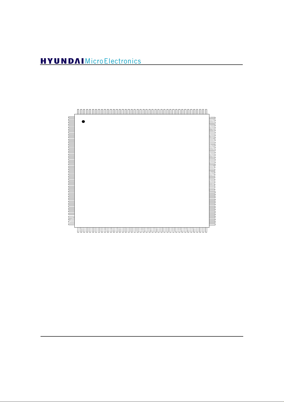
Figure 1. Pin Description
Page 6
(Package : 176TQFP)
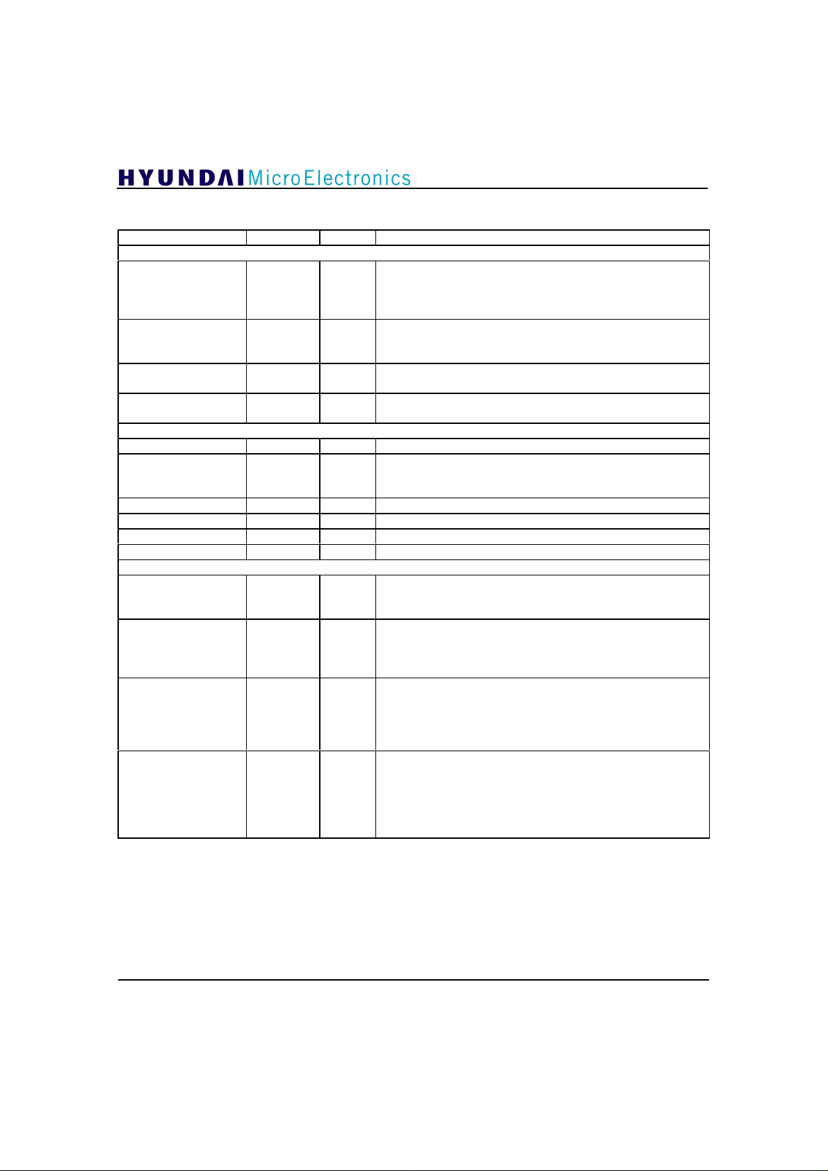
NAME PIN TYPE DESCRIPTION
CLOCK
CLOCK_27M
CLOCK_OUT
\RESET
TEST
TA[9:0]
TDI
TWEB
TDO0
TDO1
P_S_MODE
FEC_DATA[7:0]
F_START
FEC_CLOCK
CLOCKS & RESET
157 I
Operation clock.
The frequency of operating clock is 27MHz and it should be
locked in encoder system clock. The clock may be supplied by
external VCXO controlled by VPWM.
69 I
27MHz clock.
It is used to count STC value. This clock may be supplied by
external VCXO controlled by VPWM.
14 O
112 I
Operation Clock Output.
For high-speed output data
Global Reset (active low)
The signal asynchronously resets the GDC21D301A.
TEST INTERFACE (for IC self-test purpose only)
26 I
46,44,16,17,
18,19,20,21,2
2,23
27 I
25 I
8 O
9 O
Test Mode
I
Test address.
TA[9] and TA[8] are respectively multiplexed with SCAN_IN1
and SCAN_MODE pins.
Test Input Data
Test Write Enable (active low)
Test Output Data0
Test Output Data1
TRANSPORT STREAM INTERFACE
28 I
FEC Data Input Mode Selection.
0: byte-parallel input mode
1: bit-serial input mode
30,31,36,37,
38,39,40,41
29 I
32 I
I
TS Data.
It is used for byte-parallel or bit-serial transfers of a coded TS
data to the device. In bit-serial mode, FEC_DATA[0] is a serial
data input for TS data.
FEC Sync Byte Indicator.
F_START is valid in bit-serial input mode only. FEC_DATA
is aligned by the byte parallel with this signal. This signal
should be activated at the first bit of the TS sync byte or every
first bit of the data byte.
FEC Data Clock.
FEC_CLOCK is used to latch a data byte or a single bit of
coded TS into the device on the rising edge. FEC_CLOCK may
be asynchronous with the device. The value of FEC_DATA is
locked into the GDC21D301A internal buffer on the rising
edge of FEC_CLOCK, if D_VALID is asserted HIGH.
GDC21D301A
7
Page 7
Pin Description (continued)
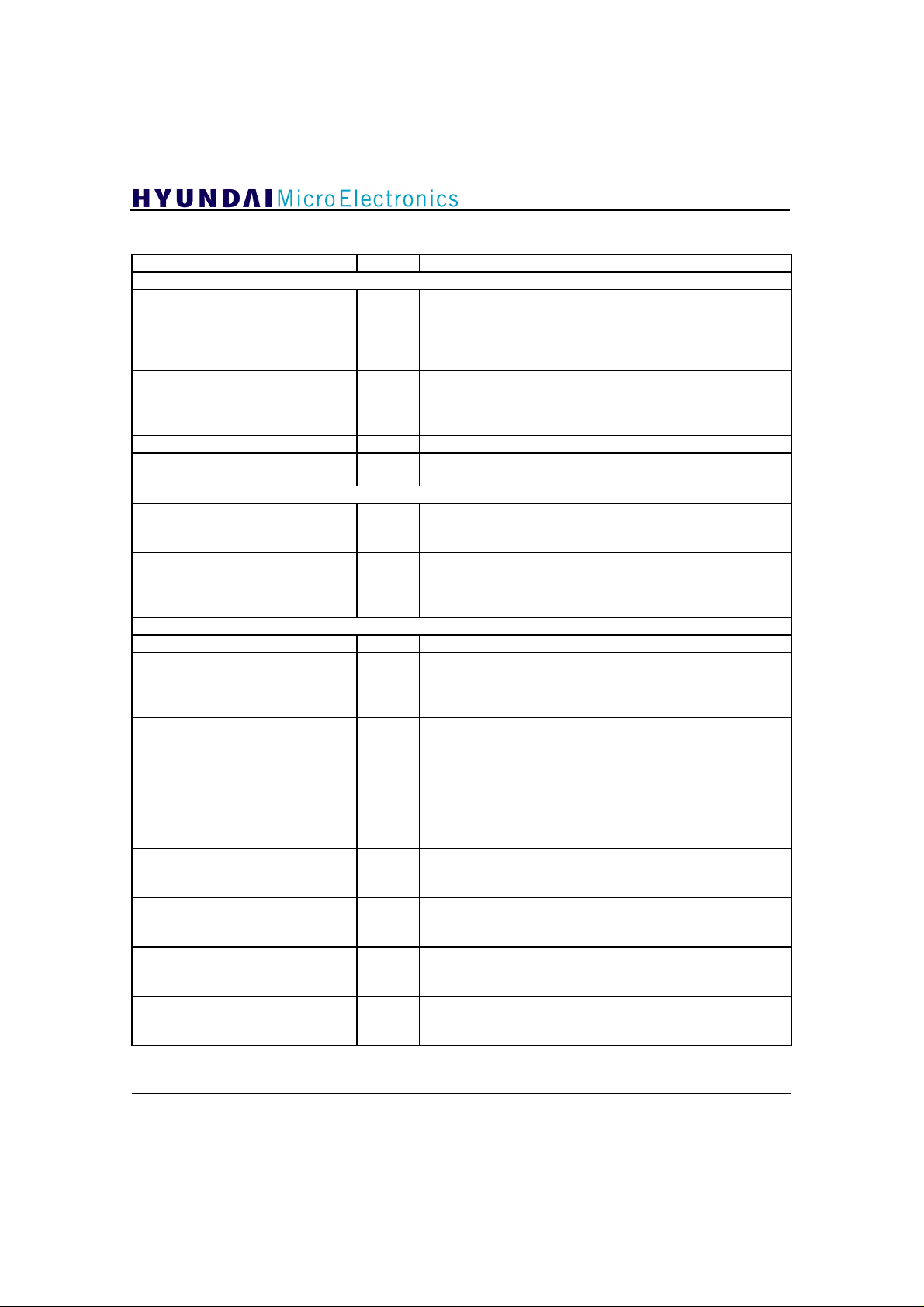
NAME PIN TYPE DESCRIPTION
\ERR_BLOCK
D_VALID
HSDEN
HIGH_SP_DATA
42 I
43 I
11 O
12, 13 O
[1:0]
VPWM
APWM
M16
DRAM_RWB
DRAM_ROW_COL_
ADDR[9:0]
126 O
101 O
47 I
49 O
50,51,52,54,
55,56,57,59,
60,61
DRAM_DATA[15:0]
67,73,74,75,
76,78,79,80,
81,83,84,85,
86,88,89,90
\DRAM_RAS0
\DRAM_RAS1
\DRAM_CAS0
\DRAM_CAS1
64 O
62 O
66 O
65 O
HIGH SPEED DATA INTERFACE
FEC Packet Error (active low).
This optional signal may be used to declare that the error has
occurred in a packet. It is used in place of
transport_error_indicator bit in the TS header by the equipment
interfacing with the GDC21D301A.
FEC Data Valid.
This signal indicates that the data value of FEC_DATA bus is
valid transport stream byte or serial bit. It will be latched in the
internal buffer on the rising edge of FEC_CLOCK.
High Speed Port Data Enable
High Speed Port Data
CLOCK RECOVERY INTERFACE
Pulse Width Modulated Pulse1.
Low pass filtered VPWM signal is fed to external VCXO for
adjusting its output frequency.
Pulse Width Modulated Pulse2.
This is used to lock the Audio clock in the Video clock for lip
synchronization. Low pass filtered APWM signal is fed to the
VCXO.
DRAM INTERFACE
DRAM 16-Mbit Configuration
DRAM Read/Write.
When you access DRAM, read mode or write mode can be
set as following.
0 : Write mode 1 : Read mode
O
DRAM Parallel Address Bus [9:0].
Row-column address is multiplexed when you access external
DRAM. For the fast page mode access, row address is applied
first, and column address is applied next.
I/O/Z
DRAM Parallel Data Bus [15:0].
DRAM Row Address Strobe0.
Select DRAM0 device. When this signal goes to low, DRAM_
ROW_COL_-ADDR[9:0] has a valid row address.
DRAM Row Address Strobe1.
Select the DRAM1 device. When this signal goes to low,
DRAM_ROW_COL_-ADDR[9:0] has a valid row address.
DRAM Column Address Strobe0.
Select the low byte DRAM data. When this signal goes to low,
DRAM_-ROW_COL_ADDR[9:0] has a valid column address.
DRAM Column Address Strobe1.
Select the high byte DRAM data. When this signal goes to low,
DRAM_-ROW_COL_ADDR[9:0] has a valid column address.
GDC21D301A
8
Page 8
Pin Description (continued)
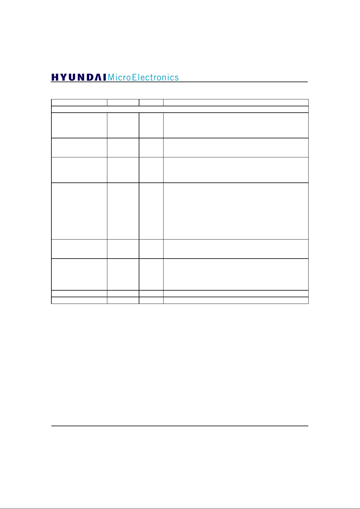
NAME PIN TYPE DESCRIPTION
\DSP_STRB
DSP_RWB
\DSP_PD
DSP_ADDR[22:0]
127 I
128 I
129 I
133,134,135,
136,137,138,
139,140,141,
142,143,144,
145,146,147,
148,149,150,
151,152,153,
154,155
BIT8MODE
DSP_DATA[15:0]
156 I
3, 2, 1, 176,
174,173,172,
171,169,168,
167,166,164,
163,162,161
DSP_READY
DSP_INT
6 O/Z
5 O
HOST PROCESSOR INTERFACE
Host Strobe (active low) : Asynchronous.
Used by the host processor to access the GDC21D301A. When
DSP_STRB signal is active, DSP_ADDR[22:0],
DSP_DATA[15:0], and DSP_PD should be valid.
Read/Write (active low) : Asynchronous.
The state of this signal defines data transfer type.
0 : Write to the device 1: Read from the device
Transport Decoder Chip Selection (active low).
This signal is used to activate and access the internal registers
of the GDC21D301A, the video decoder, the audio decoder, the
data decoder, and DRAM.
I
Host Address Bus.
These signals are connected to the address bus of the host
processor interfaced with the GDC21D301A, the video
decoder, the audio decoder, the data decoder, and DRAM.
0x4FFFFF ~ 0x4C0000 : Transport Decoder address space
0x5BFFFF ~ 0x480000 : Video decoder space
0x47FFFF ~ 0x440000 : Audio decoder space
0x43FFFF ~ 0x400000 : Auxiliary data decoder space
0x3FFFFF ~ 0x000000 : DRAM space
Host Interface Mode Selection.
0 : 16-bit data bus interface
1 : 8-bit data bus interface
I/O/Z
Host Data Bus.
These signals are connected to the address bus of external host
processor.
Data Acknowledge (active high)
Interrupt Request (active high)
GDC21D301A
9
Page 9
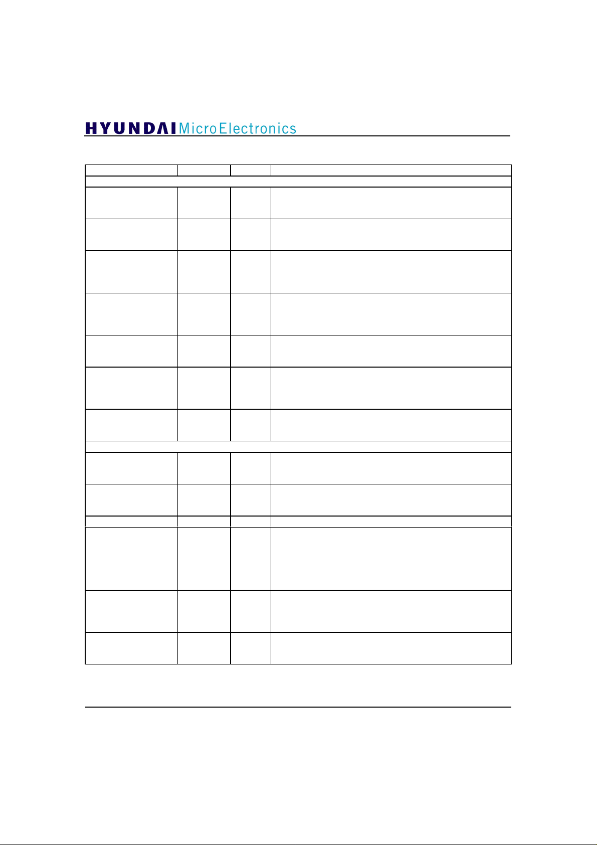
Pin Description (continued)
NAME PIN TYPE DESCRIPTION
\VID_WAIT
\VID_REQ
\VID_STRB
\VID_DCS
VAD_DATA[7:0]
PTS_DTS_STRB
BOF_V
\AUD_WAIT
\AUD_REQ
AUD_SER_DATA
\AUD_STRB
\AUD_DCS
BOF_A
95 I
96 I
125 O
123 O
110,114,115,
116,117,119,
120,122
109 O
99 I
95 I
94 I
104 O
105 O
103 O
98 I
VIDEO DECODER INTERFACE
Video Wait (active low).
This signal indicates that the access of registers in the video
decoder is ready.
Video Compressed Data Request (active low).
A video decoder requests video data from the GDC21D301A
by using this signal.
Video Compressed Data Strobe (active low).
The signal indicates that the video data in VAD_DATA[7:0]
exists. The video decoder should latch the video data on the
rising edge of VID_STRB.
Video Chip Select (active low).
This signal activates data transfers between the video decoder
and the host processor. Host processor can access the registers
of the video decoder.
I/O/Z
Video/Audio Decoder Data.
Parallel bit stream output of compressed audio, video, and
auxiliary data.
Video PTS/DTS Strobe (active high).
When this signal is asserted High, the GDC21D301A puts PTS
(Presentation_Time_Stamp) or DTS (Decoding_Time_Stamp)
into VAD_DATA[7:0] bus.
Begin of Frame0.
On the rising edge of this signal, STC, the counted PCR value,
is copied to STC3_reg.
AUDIO DECODER INTERFACE
Audio Wait (active low).
This signal indicates that the access of registers in the audio
decoder is ready.
Audio Data Request (active low).
An audio decoder requests audio data from the GDC21D301A
by using this signal.
Audio Serial Data.
Audio Data Strobe (active low).
This signal indicates that audio data on VAD_DATA[7:0]
exists. \AUD_STRB signal can be used as the data clock for
serial and parallel data transmission. Thus, if output mode is
parallel, \AUD_STRB is 1-byte strobe. And if output mode is
serial, \AUD_STRB is 1-bit strobe.
Audio Select (active low).
This signal activates data transfers between the audio decoder
and the host processor. Host processor should communicate
data with the audio decoder through the GDC21D301A.
Begin of Frame1.
On the rising edge of this signal, STC, the counted PCR_value,
is copied to STC3_reg.
GDC21D301A
Page 10
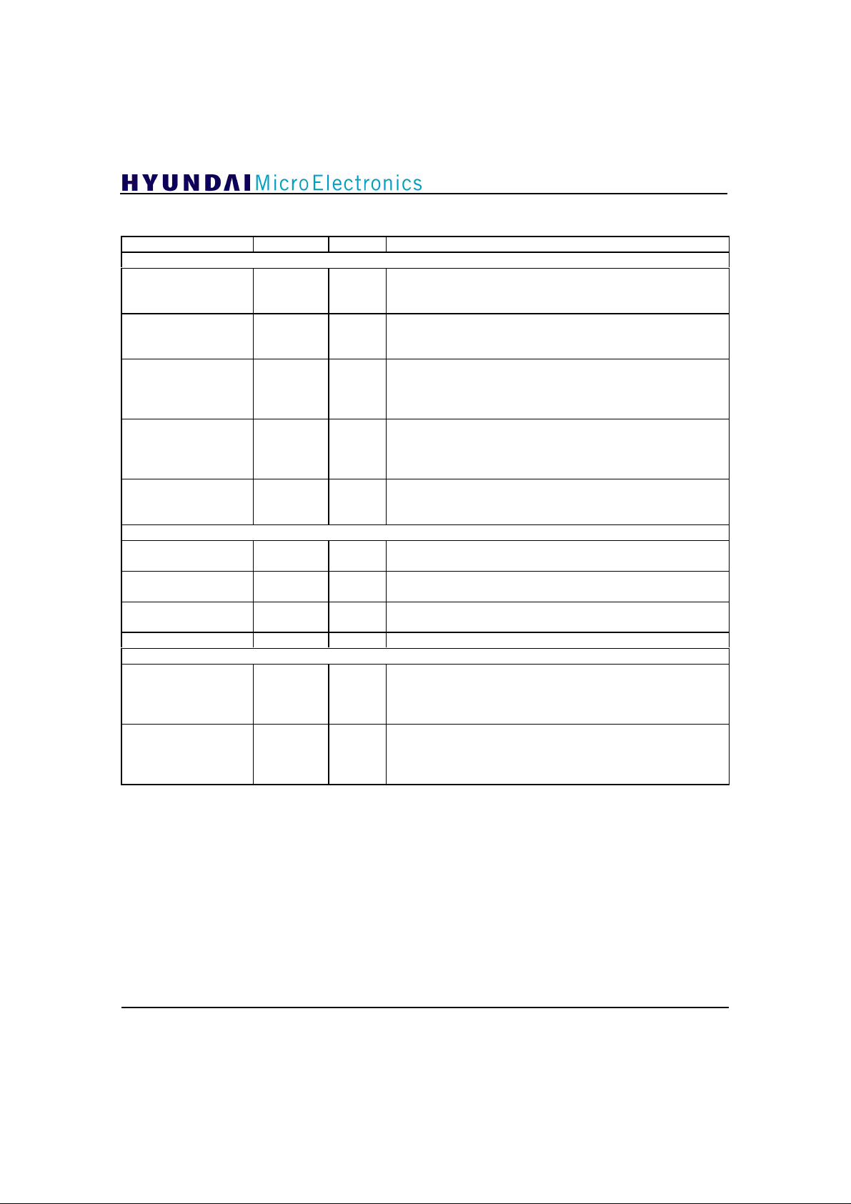
Pin Description (continued)
NAME PIN TYPE DESCRIPTION
\DATA_WAIT
\DATA_REQ
\DATA_STRB
\DATA_DCS
BOF_D
SCAN_MODE
SCAN_TEST
SCAN_IN1
SCAN_OUT1
VDD
91 I
92 I
108 O
107 O
97 I
44 I
45 I
46 I
111 O
7, 10, 33, 48,
58,68,70,82,
100,113,121,
124
VSS
4,15,24,35,
53,63,72,77,
87,102,106,
118,130
AUXILIARY DATA DECODER INTERFACE
Auxiliary Data Wait (active low).
This signal indicates that the access of registers in the auxiliary
decoder is ready.
Auxiliary Data Request (active low).
This signal is asserted when an auxiliary device requests data
from the GDC21D301A.
Auxiliary Data Strobe (active low).
This signal qualifies data contained in VAD_DATA[7:0]. This
auxiliary decoder should latch the auxiliary data on the rising
edge of DATA_STRB.
Auxiliary Select (active low).
This signal activates data transfers between the auxiliary
decoder and the host processor. Host processor can access the
registers of the auxiliary decoder.
Begin of Frame2.
On the rising edge of this signal, STC, the counted PCR value,
is copied to STC3_reg.
SCAN TEST
Scan Test Mode Enable Input.
It has to be connected to VSS level.
Scan Test Mode Enable Input.
It has to be connected to VSS level.
Scan-path Input on Scan Test Mode.
It has to be connected to VSS level.
Scan-path Output on Scan Test Mode
POWER AND GROUND
PWR
GND
3.3 V Power Supply
Ground
GDC21D301A
11
Page 11
4. Block Diagram
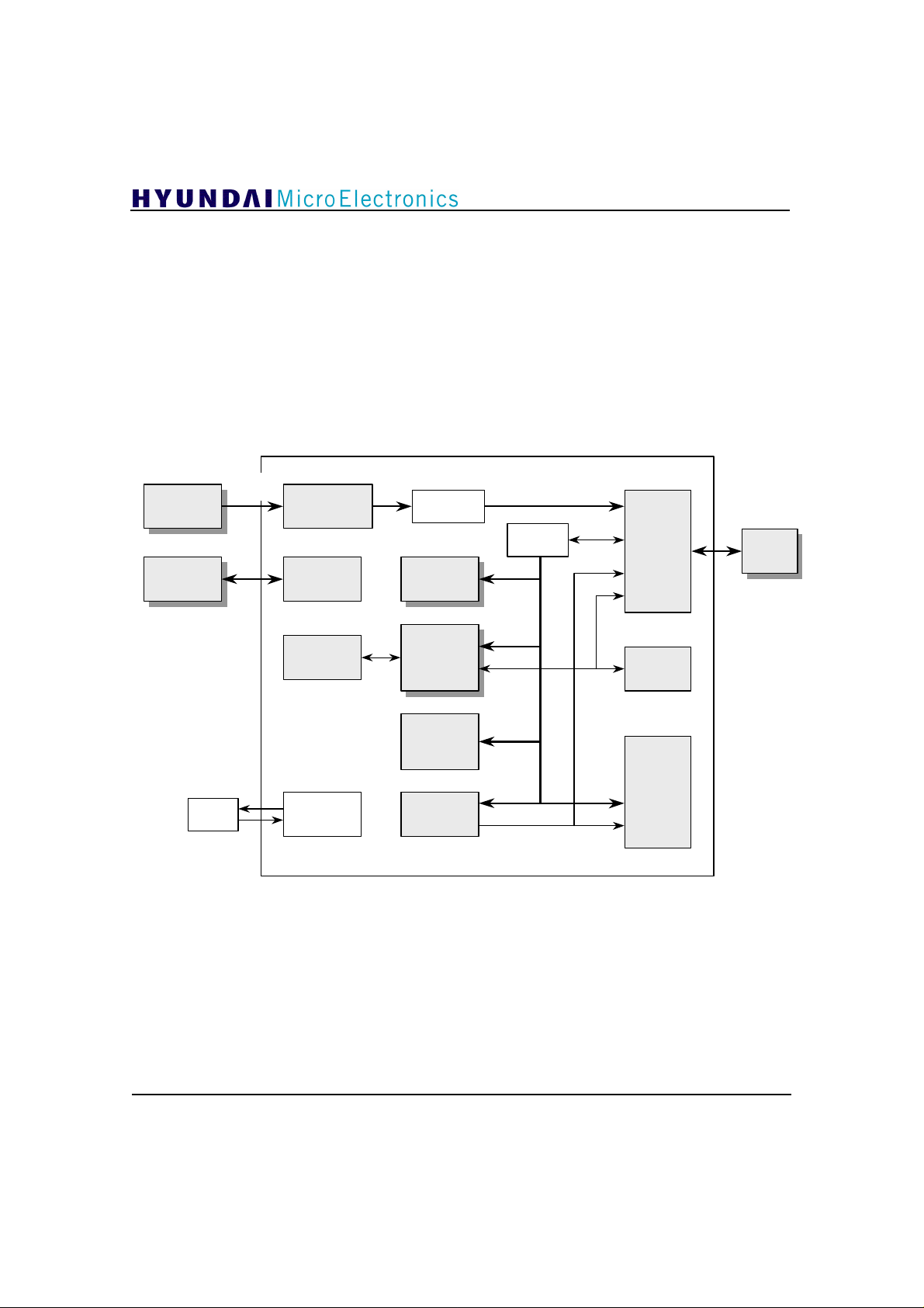
The figure 2 shows the internal block diagram of
the GDC21D301A. This chip receives the byteparallel/bit-serial transport data from
FEC(Forward-Error-Correction) device, and stores
the whole data into DRAM. After decoding the
transport data in DRAM, it de-multiplexes audio,
video, and auxiliary data packets, and transfers
them into the corresponding decoder devices
Transport
FEC
Decoder
8/16bit
8/16bit
MCU
MCU
Stream
FEC
Interface
Host
Interface
TS Buffer
Sync
Detect
GDC21D301A
through the decoder interface blocks. The host
processor can control the GDC21D301A and
access the decoder devices and DRAM through the
host interface. The GDC21D301A generates PWM
pulses to control the frequency of system clock and
audio clock. The pulse width of PWM can be
programmed by the host processor.
Buffer
Memory
Controller
4Mb
DRAM
TS Header
Decode
Adaptation
Field
Decode
PES
Decode
High-speed
Interface
External
Decoder
Interface
VCXO
PID
Memory
Clock
Control
Figure 2. The Block Diagram of the Transport Decoder
12
Page 12

5. Functional Description
5.1 Forward-Error-Correction (FEC)
Interface
The GDC21D301A can receive Transport Stream
packets in byte-parallel or bit-serial mode. FEC
Interface block gets these TS data, and temporarily
saves them in the internal buffer(TS Buffer).
In bit-serial mode, F_START should be
activated(high) when the most significant bit or the
first bit of each packet is fed. \ERR_BLOCK pin is
used to indicate valid packet, and D_VALID pin to
indicate valid TS data (it should be deactivated at
parity bits). TS data is fed on the rising edge of
FEC_CLOCK.
5.2 Sync Detector
This block searches the sync byte of TS
packet(0x47) at Sync Hysterisis register during
specified time. If it detects correct sync data, then
TS Header Decoder block takes control of
decoding process.
GDC21D301A
5.3 TS Header Decoder
This block decodes Transport Stream header and
determines if packet should be decoded further by
comparing PID with the values in internal PID
memory. PSI data is stored in external DRAM, and
can be read by the host processor. If high speed out
enable(Hig) bit in PID registers is activated, the
whole corresponding TS data are output to highspeed ports (refer to Register Description section).
5.4 Adaptation Field Decoder
Refer to the Register Description section
5.5 PES Decoder
This block decodes PES header and de-multiplexes
payload data to appropriate parts (refer to Register
Description section).
Audio and auxiliary data are stored in DRAM,
re-read by the GDC21D301A, and sent to
external decoder. But video data is directly
output to the external decoder.
13
Page 13
5.6 Memory Controller
GDC21D301A
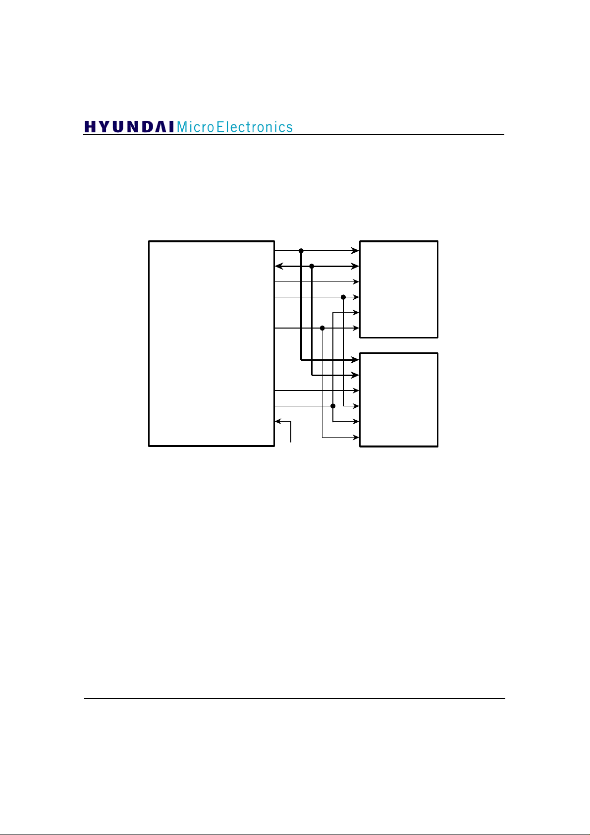
This controls DRAM interface. It refreshes
DRAM, writes and reads data to and from
DRAM. The corresponding addresses where
the data is written and read are stored in
GDC21D301
DRAM_ADDR[9:0] ADDR[9:0]
DRAM_DATA[15:0] DATA[15:0]
\DRAM_RAS0
\DRAM_CAS0
DRAM_RWB RWB
\DRAM_RAS1
\DRAM_CAS1
Figure 3. External DRAM Interface
M16
pointer memory by the Host processor. The
GDC21D301A requires one or two DRAMs
(256Kx16b or 1Mx16b).
DRAM 0
(256Kx16 or 1Mx16)
\RAS
\LCAS
\UCAS
DRAM 1
ADDR[9:0]
DATA[15:0]
\RAS
\LCAS
\UCAS
RWB
5.7 High-Speed Interface
This is an interface block of external high-speed
ports which send whole TS packets.
5.8 External Decoder Interface
This reads data from buffer and sends it to the
corresponding external decoder. It also controls the
input/output of data to and from external decoder.
5.9 Host Interface
Host Processor can access external decoders
through the GDC21D301A transport decoder.
DSP_DATA[15:0] ports are used for data bus.
14
To access one of the external decoders through the
GDC21D301A, host address bus
(DSP_ADDR[22:0]) should be as follows.
For video decoder access,
DSP_ADDR[22:18] = “100 11”.
For audio decoder access,
DSP_ADDR[22:18] = “100 01”.
For auxiliary decoder access,
DSP_ADDR[21:18] = “100 00”.
5.10 Clock Controller
It outputs two PWM signals(VPWM and APWM)
which can be controlled by the Host Processor. The
PWM signals can be used to control external
VCXOs.
Page 14
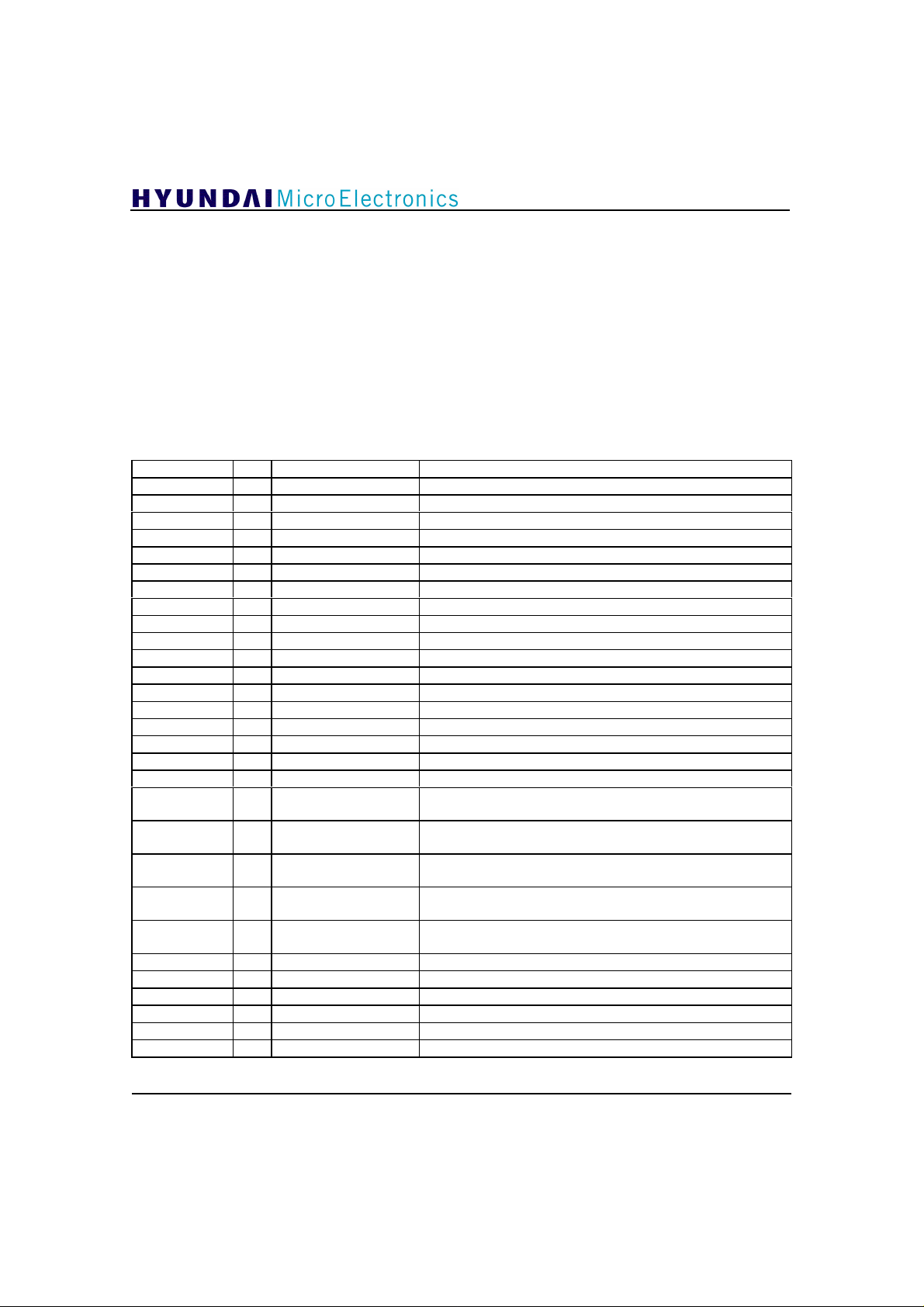
6. Register Description
This chapter describes the registers in the
GDC21D301A. Table 1 summarizes these registers.
Note the following general information:
• All registers are 16-bit wide and can read/write
unless especially noted.
• All accesses to internal registers are allowed by
word or byte using DSP_ADDR[0] pin which
determines access mode unit.
Table 1. Register Summary
ADDR[A10:A0] R/W REGISTERS DEFINITION
000
002
004
006
008
00a
00c
00e
010
012
014
02a ~ 02e
030 ~ 034
036 ~ 03c
040
042,044
046
048
060,062
064,066
068,06a
06c,06e
070,072
400,402
404,406
408,40a
40c,40e
410 ~ 47a
47c,47e
R/W Interrupt Flag 1 Indicates active interrupts
R/W Interrupt Flag 2 Indicates active interrupts
R/W Interrupt Mask 1 Interrupt Enable
R/W Interrupt Mask 2 Interrupt Enable
R/W Instruction Controls the decoding
R/W Round Buffer Controls Buffer Management
R PID Flag 1 Current Packet transferred
R PID Flag 2 Current Packet transferred
R/W PWM control 1 Controls PWM output
R/W PWM control 2 Controls PWM output
R/W Sync Hysterisis Sets lock/unlock parameters for sync detect
R PTS PTS of Current Packet transferred
R DTS DTS of Current Packet transferred
R PCR PCR of Current Packet transferred
R splicing_count_ down Current Splicing Countdown transferred
R ES_rate Current ES rate transferred
R DSM_trick_mode Current DSM trick mode transferred
R additional_copy_info Additional copy information
R STC 1 STC register contains the instant value of internal STC counter
when new PCR is transferred.
R STC 2 STC register contains the instant value of internal STC counter
when the beginning of frame signal(BOF1) is detected.
R STC 3 STC register contains the instant value of internal STC counter
when the beginning of frame signal(BOF2) is detected.
R STC 4 STC register contains the instant value of internal STC counter
when the beginning of frame signal(BOF3) is detected.
R STC 5 STC register contains the instant value of internal STC counter
when STC fetch instruction is activated.
R/W Vid PID (0) Assigns Video PID
R/W Aud PID (1) Assigns Audio PID
R/W Aux PID (2) Assigns Auxiliary PID
R/W PSI_3 PID Assigns PSI_3 PID
R/W PSI_4 ~ PSI_30 PID Assigns PSI_4 ~ PSI_30 PID
R/W PSI_31 PID Assigns PSI_31 PID
• The reserved bits should be written to zero to
preserve compatibility with future features.
• Register addresses that are not defined in Table 1
are reserved. Read from these locations causes
unpredictable results. It is recommended not to
access these registers.
• In order to access these register, you should
set DSP_ADDR[22:18] to “100 11”.
GDC21D301A
15
Page 15
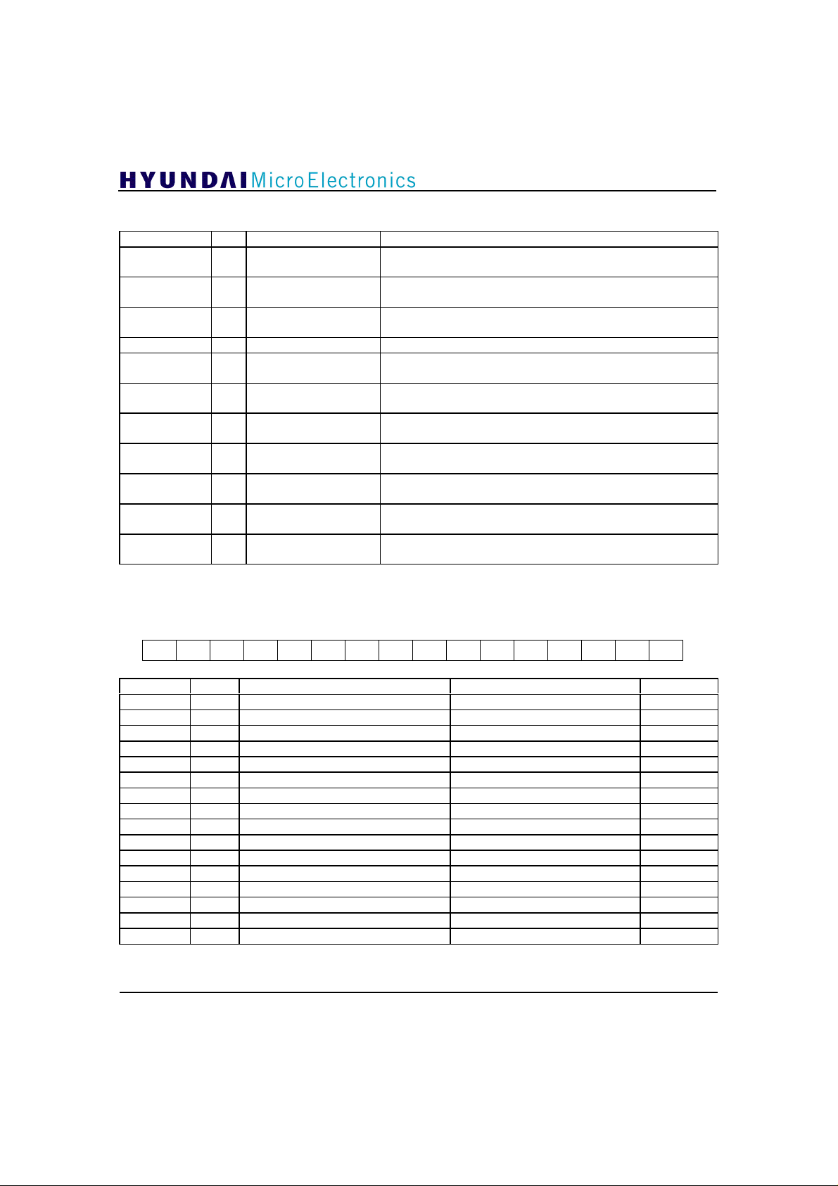
Table 1. Register Summary (continued)
Dci
Rai
Epi
Pcf
Opf
Spf
Tpf
Aef
Cef
Xpf
Vpf
Apf
Psh
Psl
Tpr
Tei
ADDR[A10:A0] R/W REGISTERS DEFINITION
618 ~ 61e
620 ~ 6f6
6f8 ~ 6fe
700 ~ 706
708 ~ 70e
710 ~ 716
718 ~ 71e
720 ~ 726
728 ~ 72e
730 ~ 736
738 ~ 73e
R/W PSI_3’s data buffer
pointer
R/W PSI_4 ~ PID_30’s data
buffer pointer
R/W PSI_31’s data buffer
pointer
R/W channel buffer pointer Start, End, Read, and Write Address
R/W audio compressed data
buffer pointer
R/W audio PES extension
data buffer pointer
R/W video PES extension
data buffer pointer
R/W auxiliary compressed
data buffer pointer
R/W auxiliary PES extension
data buffer pointer
R/W transport_private_data
buffer pointer
R/W adf_extension_data
buffer pointer
Start, End, Read, and Write Address
Start, End, Read, and Write Address
Start, End, Read, and Write Address
Start, End, Read, and Write Address
Start, End, Read, and Write Address
Start, End, Read, and Write Address
Start, End, Read, and Write Address
Start, End, Read, and Write Address
Start, End, Read, and Write Address
Start, End, Read, and Write Address
GDC21D301A
Interrupt Flag 1 (0x000)
15 8 7 0
FIELD BITS DESCRIPTION VALUES DEFAULT
Dci 15 discontinuity_indicator
Rai 14 random_access_indicator
Epi 13 elementary_stream_priority_indicator
Pcf 12 PCR_flag
Opf 11 OPCR_flag
Spf 10 splicing_point_flag
Tpf 9 transport_private_flag
Aef 8 adaptation_field_extension_flag
Cef 7 continuity counter error
Xpf 6 auxiliary packet comes
Vpf 5 video packet comes
Apf 4 audio packet comes
Psh 3 one of PSI16 ~ PSI_31 packets comes
Psl 2 one of PSI3 ~ PSI_15 packets comes
Tpr 1 transport_priority
Tei 0 transport_error_indicator
16
Page 16
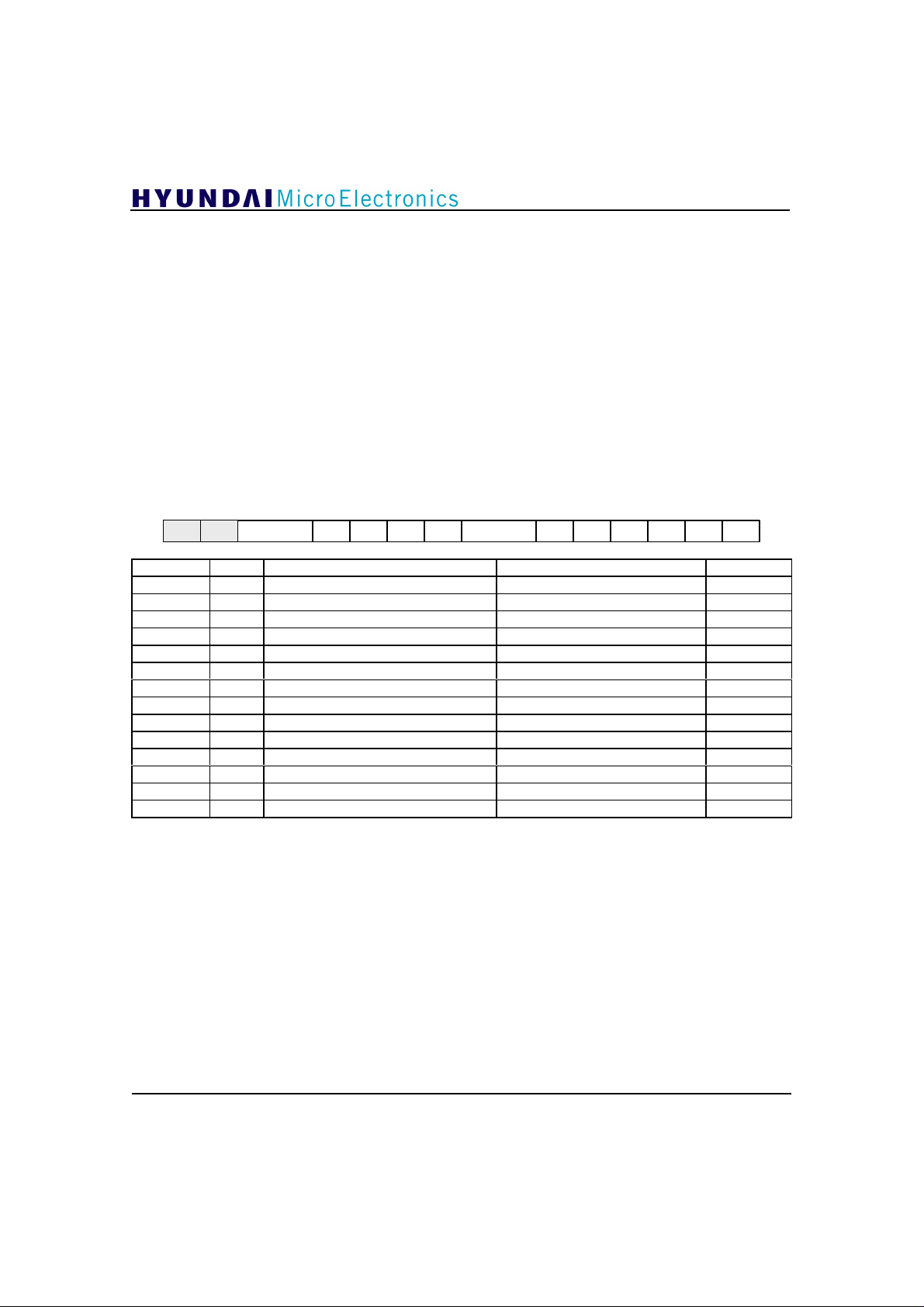
Interrupt Flag 2 (0x002)
Psc
Ppr
Dai
Cpr
Ooc
Pdf
Esf
Erf
Dtf
Acf
Crf
Pef
Sdr
Slk
GDC21D301A
When an interrupt condition occurs, the
corresponding bit in Interrupt Flag registers are
asserted 1. Whenever a bit in the Interrupt Flag is 1,
the corresponding bit in Interrupt Mask registers is
set to 1, the Ien bit in the Instruction register to 1,
and the GDC21D301A asserts DSP_INT, the
external interrupt signal. Note that the occurrence
of an interrupt condition always causes the
corresponding bit in Interrupt Flag registers to be
set, even if the condition is disabled(i.e., the
corresponding bit in Interrupt Mask registers is
set to 0).
Interrupt Flag 1, 2 registers are cleared by the
15 8 7 0
FIELD BITS DESCRIPTION VALUES DEFAULT
Slk 15 Sync_lock
Sdr 14 Sync_drop
Psc 13:12 PES_scrambling_control
Ppr 11 PES_priority
Dai 10 data_alignment_indicator
Cpr 9 copyright
Ooc 8 original_or_copy
Pdf 7:6 PTS_DTS_flag
Esf 5 ESCR_flag
Erf 4 ES_rate_flag
Dtf 3 DSM_trick_mode_flag
Acf 2 additional_copy_info_flag
Crf 1 PES_CRC_flag
Pef 0 PES_extension_flag
Host whenever they are read, and DSP_INT is
deasserted.
In the GDC21D301A, Slk and Sdr is added to
indicate the state of Sync. The GDC21D301A first
searches Sync byte from transport stream. If the
device succeeds in finding 0x47, it writes
Slk(Sync_lock) bit in Interrupt flag 2 register. Until
sync is detected, Sdr flag maintains active high
state, so the host processor can monitor whether
Sync(0x47) is detected or not.
All bits except Slk and Sdr are set when packet is
matched to PID register.
Interrupt Mask 1 (0x004)
All bits respectively correspond with each ones in
Interrupt Flag 1 register.
1 = Interrupt enabled
Interrupt Mask 2 (0x006)
All bits respectively correspond with each ones in
Interrupt Flag 2 register.
1 = Interrupt enabled
17
Page 17
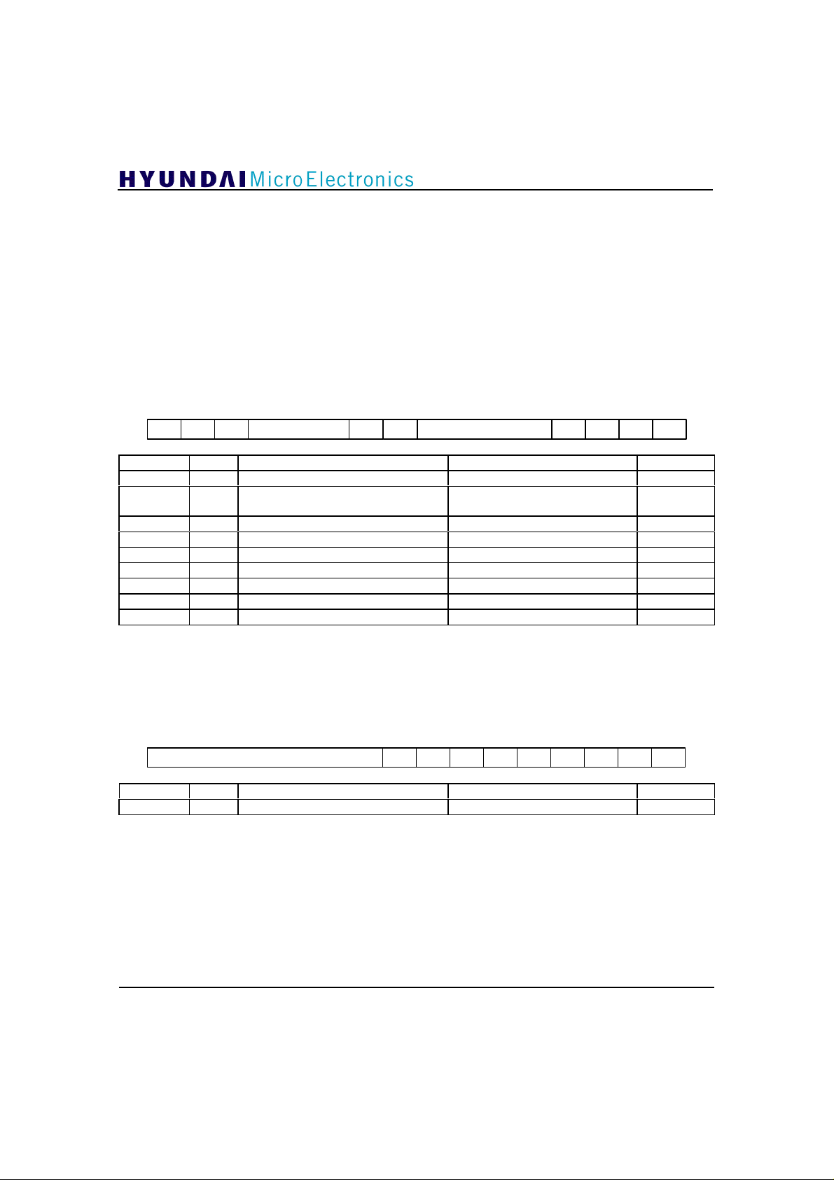
Instruction (0x008)
GDC21D301A
When error(discontinuity) happens in video packet,
i.e., in case Sec=‘1’, the GDC21D301A inputs
video sequence error code in data output.
In case Aps=‘0’, the GDC21D301A outputs audio
compressed data in parallel mode, and in case
Aps=‘1’, the GDC21D301A outputs the data in
serial mode through AUD_SER_DATA pin.
When Vts is 1, the GDC21D301A inputs PTS and
DTS data before sending them to video packet
according to Pdf flag bit of Interrupt Flag 2
register. When Ucb is 1, the GDC21D301A
15 8 7 0
receives data from channel input.
When Ice is 1, the GDC21D301A ignores channel
empty condition(i.e., the GDC21D301A continues
decoding data in channel buffer whether they were
decoded before or not.).
When Stc is 1, the GDC21D301A loads internal
PCR counter to STC5 register, and then this bit is
cleared automatically. In case Lst is 1, the
GDC21D301A loads internal PCR counter with
new value when next PCR value is loaded in the
packet, and then this bit is cleared automatically.
Sec Vts Ice Stc Lst Den IenAps Ucb
FIELD BITS DESCRIPTION VALUES DEFAULT
Sec 15 Sequence_error_code 1=sequence_error_code inserted
Aps 14 Audio parallel/serial output 0=parallel
1= serial
Vts 13 Video PTS,DTS output 1=PTS/DTS inserted
Ucb 9 Update channel buffer
Ice 8 Ignore channel empty
Stc 3 load STC5
Lst 2 load PCR
Den 1 Global decoding enable 1=decoding enable
Ien 0 Global Interrupt enable 1=interrupt enable
Round Buffer (0x00a)
When Rpn is 1, write pointer is reached to end
pointer, and the write pointer is changed to start
15 8 7 0
pointer(i.e., the GDC21D301A overwrites the
following data).
Rp8 Rp4 Rp3 Rp2 Rp1 Rp0Rp7 Rp6 Rp5
FIELD BITS DESCRIPTION VALUES DEFAULT
Rpn 8:0 Round the buffer of the PSI_n
18
Page 18
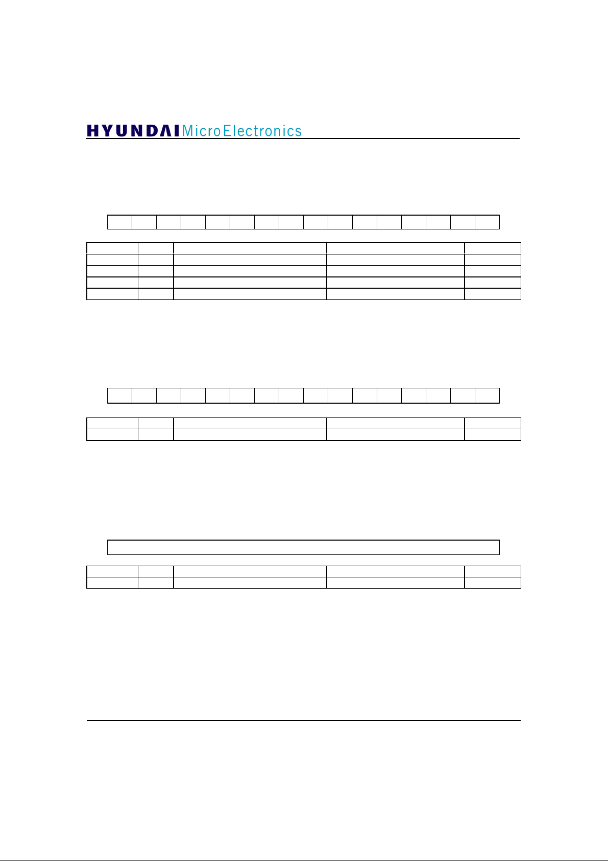
PID Flag 1 (0x00c)
GDC21D301A
When the GDC21D301A decodes the packet
whose PID is activated for decoding, it sets the
15 8 7 0
corresponding bit in PID Flag 1, or 2 register.
P15 P14 P13 P12 P11 P10 P9 P8 P7 P6 P5 P4 P3 P2 P1 P0
FIELD BITS DESCRIPTION VALUES DEFAULT
P15 ~ P3 15:3 PID flag for PSI_15 ~ PSI_3
P2 2 Auxiliary PID flag
P1 1 Audio PID flag
P0 0 Video PID flag
PID Flag 2(0x00e)
These bits indicate the type of the packet
which the GDC21D301A is now decoding.
15 8 7 0
P31 P30 P29 P28 P27 P26 P25 P24 P23 P22 P21 P20 P19 P18 P17 P16
FIELD BITS DESCRIPTION VALUES DEFAULT
P31 ~ P16 15:0 PID flag for PSI_31 ~ PSI_16
APWM control (0x010)
APWM output signal is generated by this value.
External VCXO for audio can be controlled by this
value and the lip synchronization between video
15 8 7 0
and audio clock. The control of this register is the
same as that of VPWM.
APWM
FIELD BITS DESCRIPTION VALUES DEFAULT
APWM 15:0 Audio PWM control 0x0000 to 0xFFFF 0x7FFF
19
Page 19
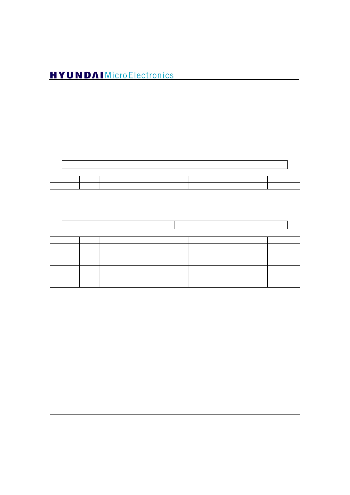
VPWM control (0x012)
GDC21D301A
The chip uses Sigma-delta modulation for VPWM
signal. Modulation clock is 1/34 system
clock(27MHz/34 = 794KHz). VPWM output signal
is generated by this value. When the register value
is 0x7FFF, the period of '1' and the period of '0'
have the same value of 0.630usec, and the cycle
time is 1.259usec, i.e., the duration of VPWM
output signal is 50%. The larger is the value greater
15 8 7 0
than 0x7FFF, the longer is the high period
generated. For example, if register value is 0x0000,
there is no data of '1' in 65536 data. Only the data
of '0' is almost uniformly distributed in 65536 data.
Adjusting PWM pulse, system VCXO can be
controlled to achieve lip synchronization or system
clocks locking.
VPWM
FIELD BITS DESCRIPTION VALUES DEFAULT
VPWM 15:0 Video PWM control 0x0000 to 0xFFFF 0x7FFF
Sync Hysteresis (0x014)
15 8 7 0
Scd
FIELD BITS DESCRIPTION VALUES DEFAULT
Scd 7:5 Sync Drop
Scl 4:0 Sync Lock
0 = should not be used
1 – 7 = The number of consecutive
sync bytes must be discarded to
constitute a sync drop.
0 = should not be used
1 – 31 = The number of consecutive
sync bytes must be detected
before sync is acquired.
Scl
0x1
0x03
20
Page 20
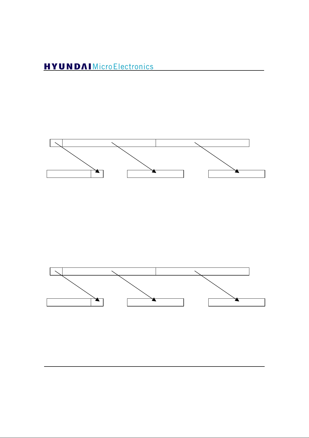
PTS (0x02a ~ 0x02e)
PTS Register 1 (0x02a)
PTS Register 2 (0x02c)
PTS Register 3 (0x02e)
GDC21D301A
These read-only registers hold the PTS value that
GDC21D301A retrieves from the transport packet
whose PID value is activated for decoding.
Current Packet’ s PTS
32 31 16 15 0
15 0 15 0 15 0
PTS 3 PTS 2 PTS 1
DTS (0x030 ~ 0x034)
DTS Register 1 (0x030)
DTS Register 2 (0x032)
DTS Register 3 (0x034)
These read-only registers hold the DTS value that
GDC21D301A retrieves from the transport packet
Current Packet’ s DTS
32 31 16 15 0
whose PID value is activated for decoding.
15 0 15 0 15 0
DTS 3 DTS 2 DTS 1
21
Page 21
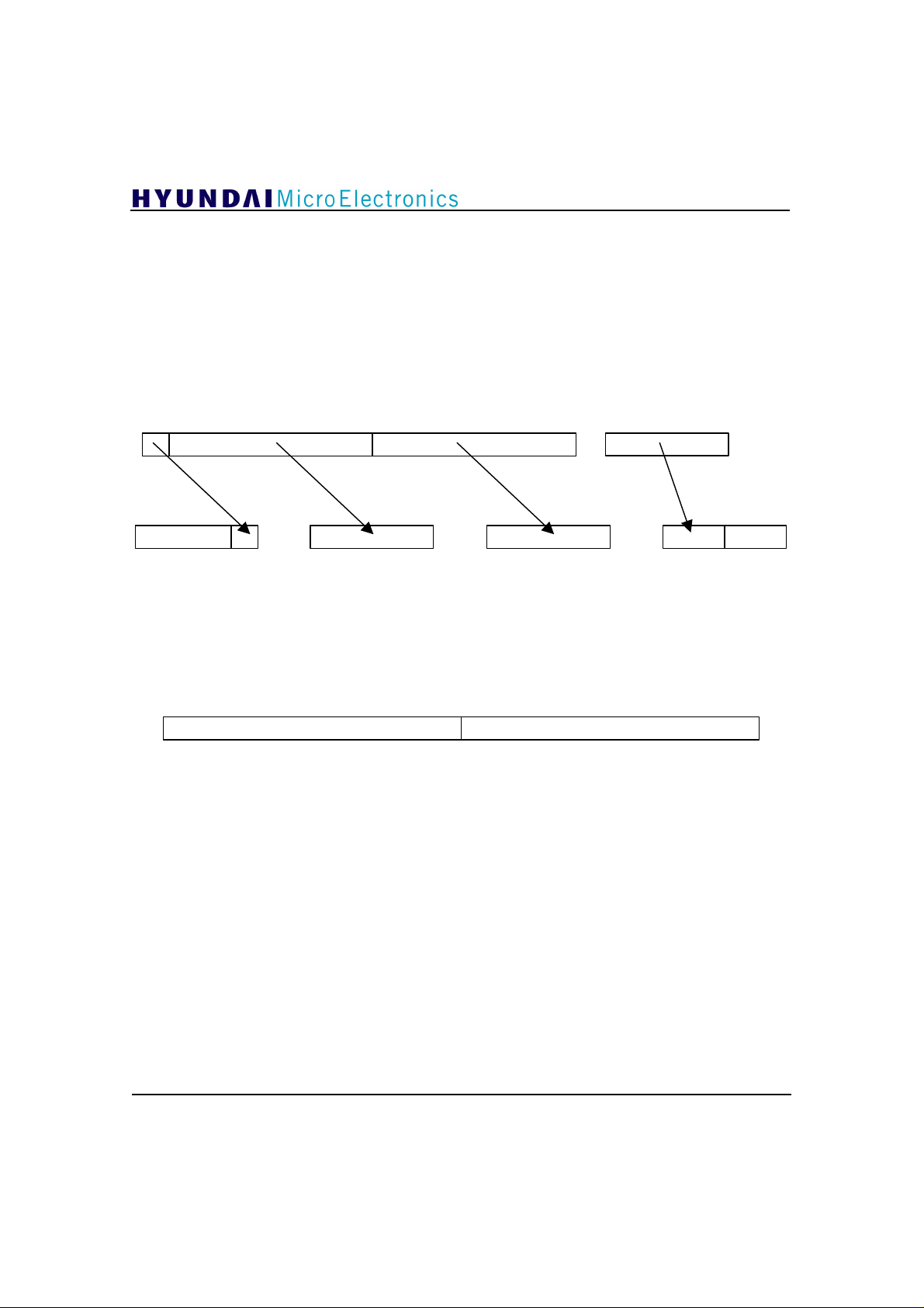
PCR (0x036 ~ 0x03c)
PCR Register 1 (0x036)
PCR Register 2 (0x038)
PCR Register 3 (0x03a)
PCR Register 4 (0x03c)
GDC21D301A
These read-only registers hold the PCR value that
the GDC21D301A retrieves from the transport
Current Packet’ s PCR_base PCR_Extension
32 31 16 15 0
packet whose PID value is activated for decoding.
8 0
15 0 15 0 15 0
PCR 3 PCR 2 PCR 1 PCR 4
Splicing_countdown (0x040)
This read-only register holds the
splicing_countdown value that the GDC21D301A
15 8 7 0
retrieves from the transport packet whose PID
value is activated for decoding.
Splicing_countdown
15 9 8 0
22
Page 22
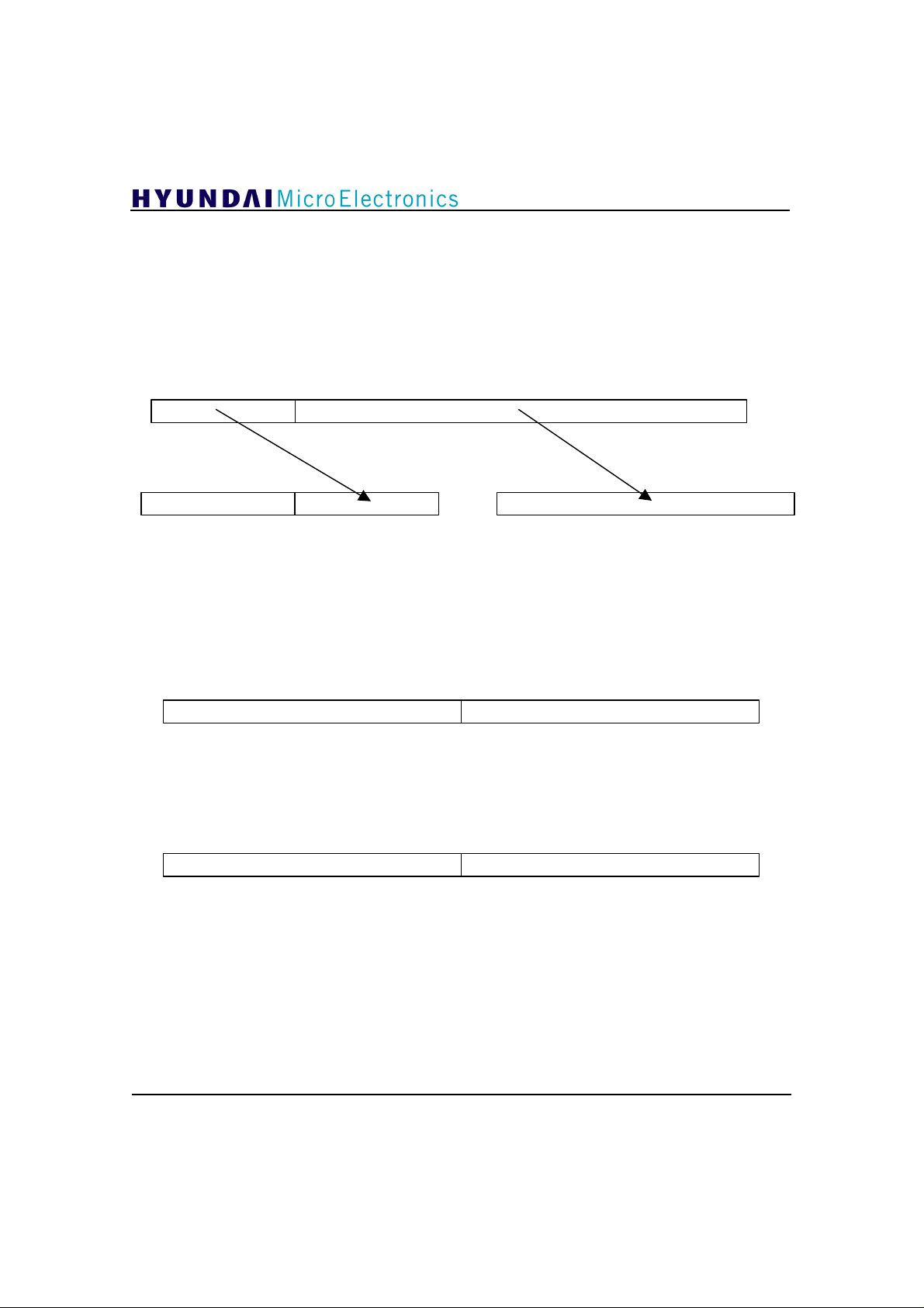
ES_rate (0x042 ~ 0x044)
ES_rate Register 1 (0x042)
ES_rate Register 2 (0x044)
GDC21D301A
These read-only registers hold the ES_rate value
that the GDC21D301A retrieves from the transport
Current Packet’ s ES_rate
21 15 0
15 6 0 15 0
ES_rate 2
5
packet whose PID value is activated for decoding.
ES_rate 1
DSM_trick_mode (0x046)
This read-only register holds the DSM_trick_mode
field that the GDC21D301A retrieves from the
15 8 7 0
transport packet whose PID value is activated for
decoding.
DSM_trick_mode
Additional_copy_info (0x048)
This read-only register holds the
additional_copy_info field that the GDC21D301A
15 8 7 0
retrieves from the transport packet whose PID
value is activated for decoding.
Additional_copy_info
23
Page 23
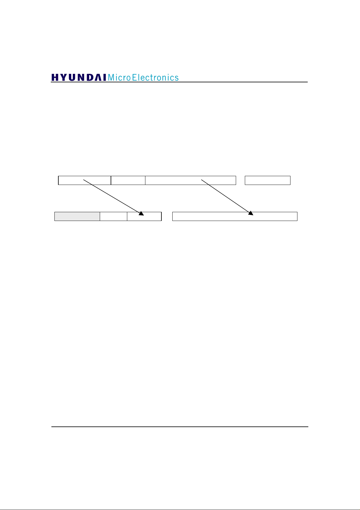
STC1 (0x060 ~ 0x062)
STC1 Register 1 (0x060)
STC1 Register 2 (0x062)
GDC21D301A
These read-only registers hold the lower 20 bits of
STC value from the internal STC counter of the
GDC21D301A when the GDC21D301A retrieves
the PCR value from the transport packet whose
PID value is activated for decoding. The internal
Internal STC counter base STC Extension
21 15 0
15 6 0 15 0
19 0 8
7 3
STC1_2
4
STC2 (0x064 ~ 0x066)
STC2 Register 1 (0x064)
STC2 Register 2 (0x066)
These read-only registers hold the lower 20 bits of
STC value from the internal STC counter of the
GDC21D301A when external BOF1 signal is
detected.
STC counter is clocked at the frequency of input
on CLOCK_27M pin (nominally 27 MHz). In the
GDC21D301A, STC_Extension is written to
STC1_2[15:7] and can be read by user. STC1 is
also read-only register.
STC1_1
STC4 (0x06c ~ 0x06e)
STC4 Register 1 (0x06c)
STC4 Register 2 (0x06e)
These read-only registers hold the lower 20 bits of
STC value from the internal STC counter of the
GDC21D301A when external BOF3 signal is
detected.
STC3 (0x068 ~ 0x06a)
STC3 Register 1 (0x068)
STC3 Register 2 (0x06a)
These read-only registers hold the lower 20 bits of
STC value from the internal STC counter of the
GDC21D301A when external BOF2 signal is
detected.
24
STC5 (0x070 ~ 0x072)
STC5 Register 1 (0x070)
STC5 Register 2 (0x072)
These read-only registers hold the lower 20 bits of
STC value from the internal STC counter of the
GDC21D301A when STC fetch instruction is
activated(see Instruction Register).
Page 24
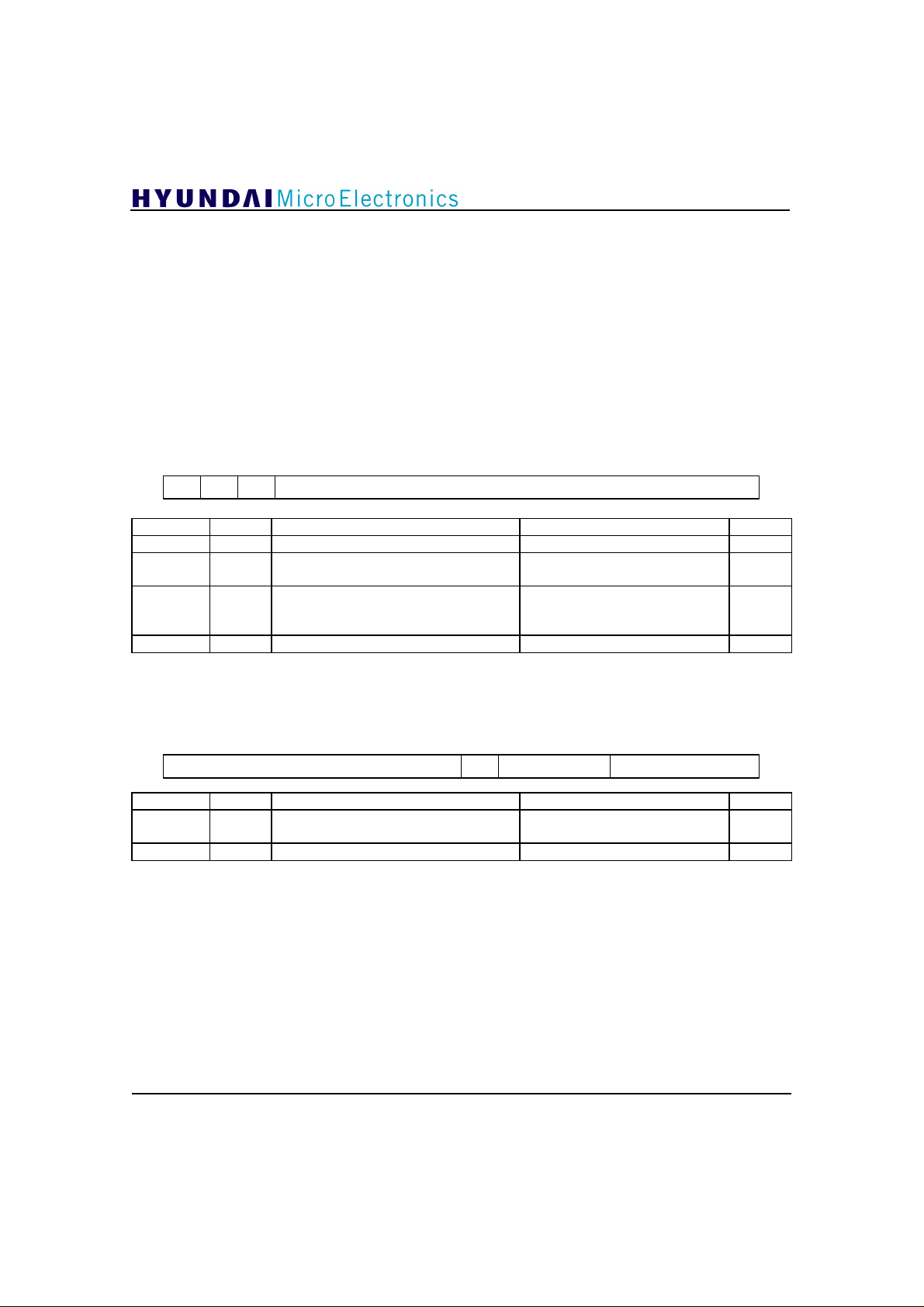
PID Registers (0x400 ~ 0x47e)
GDC21D301A
These registers should be written with certain
values during initialization phase, because the
values are undefined at first. Video, audio, and
auxiliary packet will be respectively transferred to
VAD_DATA port with VID_STRB, AUD_STRB,
and DATA_STRB signal in case Hig bit in the
register is ‘0’(i.e. High Speed Port has the highest
priority. This is equally applied to other packets.).
Other data will be transferred to the corresponding
buffer in DRAM.
Vid PID Register (0x400, 0x402)
These registers should be written with certain
values during initialization phase, because the
15 8 7 0
values are undefined at first. For correct processing,
Dst should be written to ‘0’.
Den Dst Frm PID
Field Bits Description Values Default
Den 15 PID enable 1 = PID matching enabled
Dst 14 Decoding state(status reg.) 1 = corresponding PID packet
occurred at least once before
Frm 13 Decoding Type 0 = transfer PES_payload to
external port
1 = transfer whole PES packet
PID 12:0 PID
These registers should be written with certain
values during initialization phase, because the
values are undefined at first.
15 8 7 0
Hig CCNT
Field Bits Description Values Default
Hig 7 High Speed out enable 1 = transfer whole TS packet to
high speed port
CCNT 3:0 Continuity Counter store continuity_counter value
Aud PID Register (0x404, 0x406)
Same as Vid PID register, but Audio packet
Aux PID Register (0x408, 0x40a)
Same as Vid PID register, but Auxiliary packet
25
Page 25
GDC21D301A
PSI PID Register (0x40c ~ 0x40e)
Same as Vid PID register, except the following.
Field Bits Description Values Default
Frm 13 Decoding Type 0 = This packet is a kind of PES.
1 = This packet is a kind of PSI.
In PES packet, there is no pointer_field.
Buffer Pointer Register (0x618 ~ 0x61e)
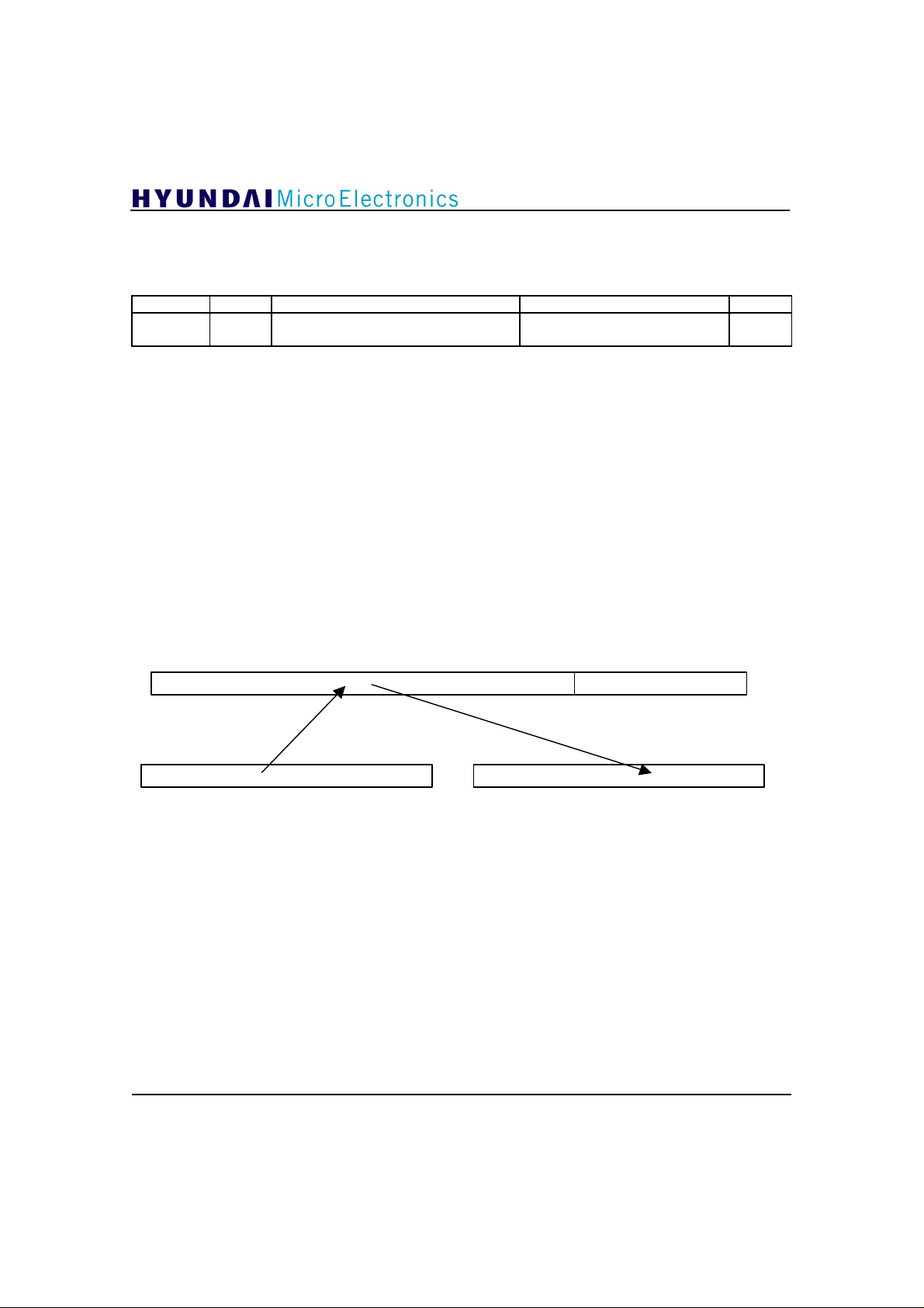
The values are undefined initially. These values are
the memory management registers for local DRAM.
These are 22-bit wide registers only whose 16 bits
can be accessed by the host.
In the following, N = n-2 and n = 3, 4, 5, ..... , 31.
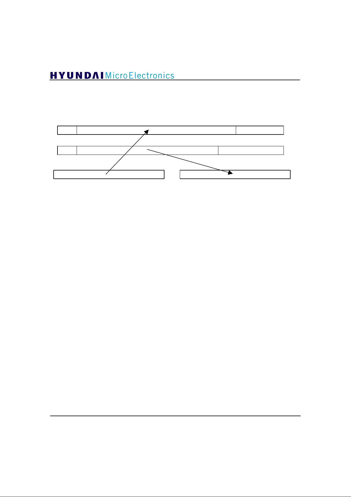
PSI_n’ s data Buffer Start Pointer Register (0x618 + 4*N)
1) When M16 = ‘ 1’ (16Mbit DRAM used)
When it is ‘Write’, the lower 6 bits are written to
Internal Start Pointer register
21 0
15
When ‘ Write’
0 15 0
6 5
When ‘ Read’
26
Page 26
GDC21D301A
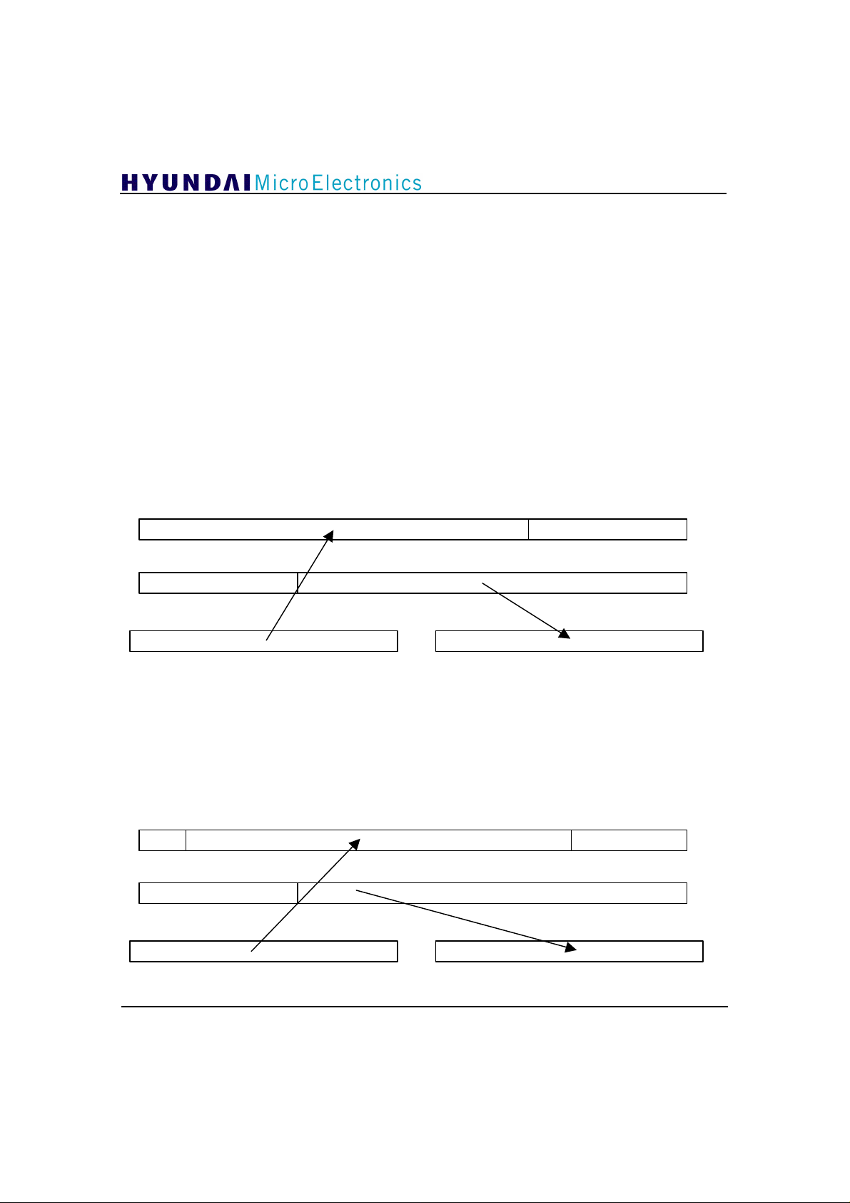
2) When M16 = ‘ 0’ (4Mbit DRAM used)
When it is ‘Write’, the lower 4 bits and higher 2 bits are written to
Internal Start Pointer register
21 0
20 19
21 06 5
15 0 15 0
When ‘ Write’
4 3
When ‘ Read’
27
Page 27
PSI_n’ s data Buffer End Pointer Register (0x61a+ 4*N)
GDC21D301A
Same as Start pointer register. But the real end
address of data buffer is one less than this register
value, for example, the real end address of PSI_4
data buffer is equal to 0x61b which is calculated by
‘0x61c minus 0x001’. The buffer size is calculated
by the following.
Size = End Pointer - Start Pointer.
PSI_n’ s data Buffer Read Pointer Register (0x61c + 4*N)
Actually this register is not used. In order to read
data in this buffer, you should access local DRAM
1) When M16 = ‘ 1’ (16Mbit DRAM used)
, and the value should be
When it is ‘Write’, the lower 6 bits are written to
located between start
and end pointer. It is recommended that the initial
Internal Read Pointer Register
21 0
21 016 15
15 0 15 0
When ‘ Write’
directly like accessing internal register.
value is the same of the start pointer. When ‘Read’,
the lower 16 bits are read.
6 5
When ‘ Read’
2) When M16 = ‘ 0’ (4Mbit DRAM used)
When it is ‘Write’, the lower 4 bits and higher 2
bits are written to ‘0’, and the value should be
located between start and end pointer. It is
recommended that this initial value is the same of
start pointer value. When ‘Read’, the lower 16 bits
are read.
Internal Read Pointer register
21 0
20 19
21 016 15
15 0 15 0
When ‘ Write’
4 3
When ‘ Read’
28
Page 28

GDC21D301A
PSI_n’ s data Buffer Write Pointer
register (0x61e + 4*N)
Same as Read pointer register. This value should
be located between start and end pointer. It is
recommended that this initial value is the same of
start pointer value. (See Round Buffer register
0x005)
Channel buffer pointer (0x700 ~ 0x706)
Same as PSI_n’s data buffer pointer register.
This buffer is used to store FEC input data. the
GDC21D301A will read the data from this buffer
to decode TS packets. The read pointer is used to
read data.
Audio compressed data buffer pointer
(0x708 ~ 0x70e)
Same as PSI_n’s data buffer pointer register.
This buffer is used to store the data which is sent to
external audio decoder. the GDC21D301A will
read the data from this buffer to send them to
external audio decoder. The read pointer is used to
read data.
Audio PES_extension data buffer
pointer(0x710 ~ 0x716)
Same as PSI_n’s data buffer pointer register.
This buffer is used to store the PES_extension data
of audio packets. Before storing the PES_extension
data, the GDC21D301A writes the size of the
PES_extension data + stuffing_bytes. The read
pointer is not used by the GDC21D301A.
Auxiliary compressed data buffer pointer
(0x720 ~ 0x726)
Same as PSI_n’s data buffer pointer register.
This buffer is used to store the data which is sent to
external auxiliary decoder. the GDC21D301A will
read the data from this buffer to send them to
external auxiliary decoder. The read pointer is used
to read data.
Auxiliary PES_extension data buffer
pointer (0x728 ~ 0x72e)
Same as PSI_n’s data buffer pointer register.
This buffer is used to store the PES_extension data
of auxiliary packets. Before storing the
PES_extension data, the GDC21D301A writes the
size of the PES_extension data + stuffing_bytes.
The read pointer is not used by the GDC21D301A.
Transport_private_data buffer pointer
(0x730 ~ 0x736)
Same as PSI_n’s data buffer pointer register.
This buffer is used to store transport_private_data
field. The read pointer is not used by the
GDC21D301A.
Adf_extension_data buffer pointer
(0x738 ~ 0x73e)
Same as PSI_n’s data buffer pointer register.
This buffer is used to store Adf_extension_data
field. The read pointer is not used by the
GDC21D301A.
Video PES_extension data buffer pointer
(0x718 ~ 0x71e)
Same as PSI_n’s data buffer pointer register.
This buffer is used to store the PES_extension data
of video packets. Before storing the PES_extension
data, the GDC21D301A writes the size of the
PES_extension data + stuffing_bytes. The read
pointer is not used by the GDC21D301A.
29
Page 29
GDC21D301A
V
DD
+ 0.33
7. Electrical Specification
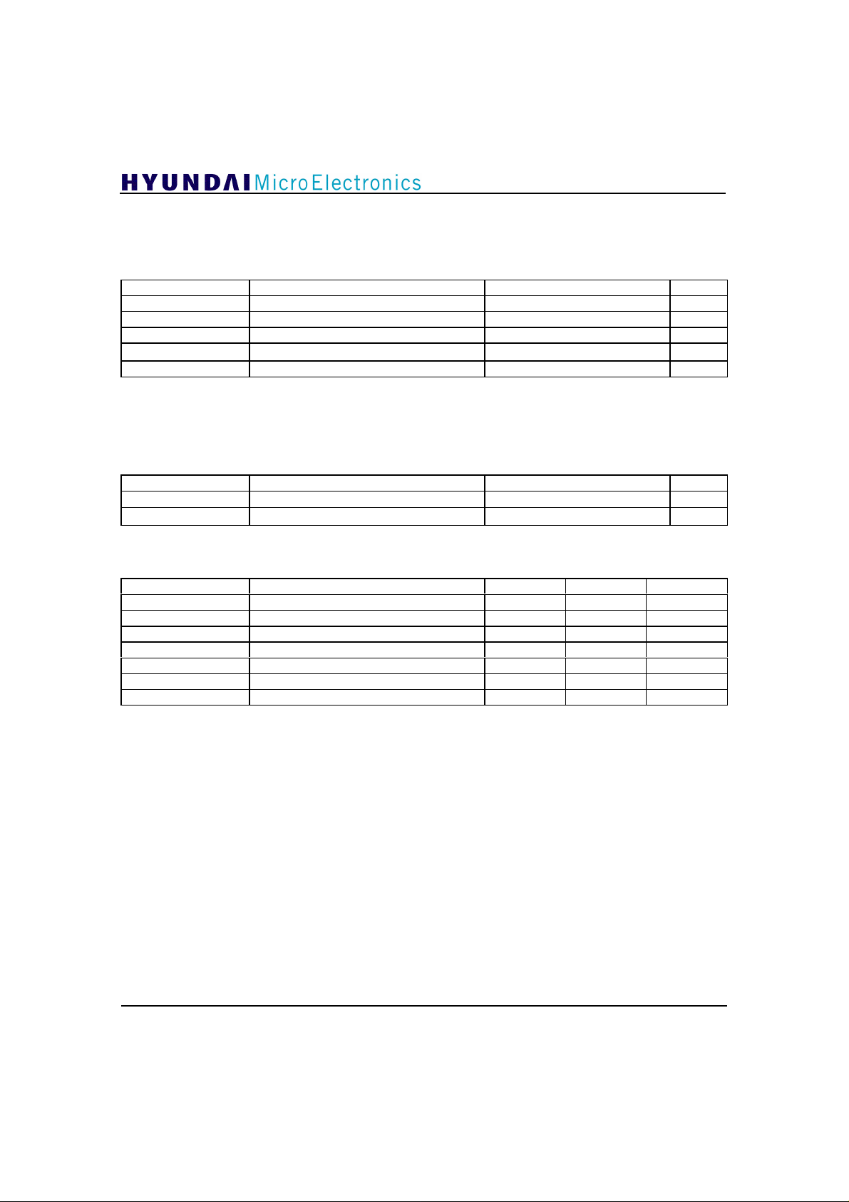
7.1 Absolute Maximum Rating
SYMBOL PARAMETERS VALUES UNIT
V
DD
V
I
Vo
T
stg
P
d
Note : Absolute Maximum Ratings means that the safety of the device cannot be
guaranteed beyond these values and it doesn’t imply that the device
should be operated within these limits.
7.2 Recommended Operating Range
SYMBOL PARAMETERS VALUES UNIT
V
DD
T
opr
7.3 DC Characteristics (VDD = 3.3 V ± 10%, TA = 0 ~ 70 °C )
SYMBOL PARAMETERS MIN MAX UNIT
V
IH
V
IL
V
OH
V
OL
I
DD
I
DDQ
F
opr
Power Supply Voltage -0.33 to 5.5 V
Digital Input Voltage -0.33 to VDD + 0.5 V
Digital Output Voltage -0.33 to VDD + 0.5 V
Storage Temperature -55 to 125
Power Dissipation 1.0 W
Power Supply Voltage
3.3 ± 10%
Operating Temperature 0 to 70
Input High Voltage 0.7 X V
Input Low Voltage -0.33 0.2 X V
Output High Voltage 2.4 V
DD
DD
DD
Output Low Voltage 0 0.4 V
Dynamic Supply Current - 150 mA
Quiescent Supply Current - 1 uA
Max. Operating Frequency - 27 MHz
¡É
V
¡É
V
V
V
30
Page 30
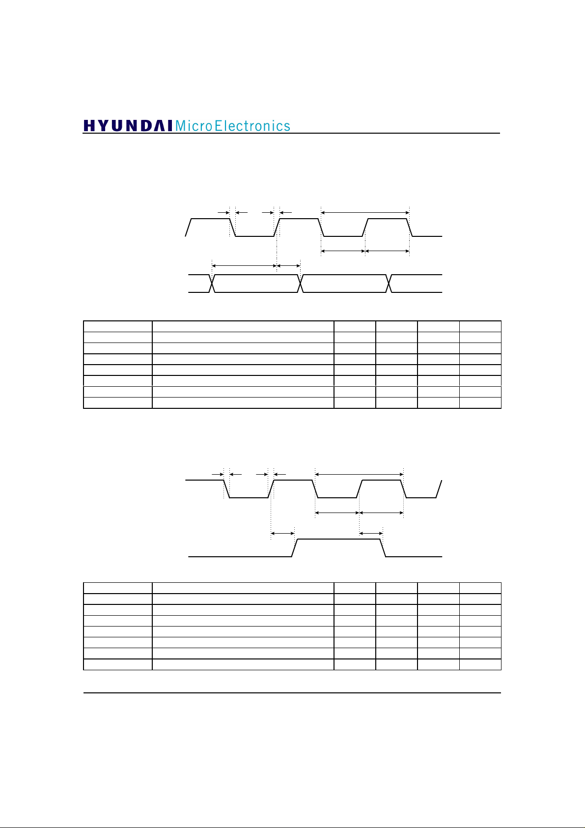
7.4 AC Characteristics (VDD = 3.3 V ± 10%, TA = 0 ~ 70 °C )
7.4.1 Transport Stream Interface Requirements
GDC21D301A
t
FCLKf
t
FCLKr
t
FCLKp
FEC_CLOCK
t
FECs
t
FECh
t
FCLKL
t
FCLKH
FEC_DATA[7:0]
D_VALID
\ERR_BLOCK
PARAMETER DESCRIPTION MIN TYP MAX UNIT
tFECh FEC_CLOCK to FEC_DATA hold time 5 - - ns
tFECs FEC_CLOCK to FEC_DATA setup time 5 - - ns
tFCLKr FEC_CLOCK rising time - - 1.5 ns
tFCLKf FEC_CLOCK falling time - - 1.5 ns
tFCLKH FEC_CLOCK high duration 10 - - ns
tFCLKL FEC_CLOCK low duration 10 - - ns
tFCLKp FEC_CLOCK period 100 - - ns
7.4.2 Clock Interface Requirements
t
CLOCKf
t
CLOCKr
t
CLOCKp
CLOCK
t
PWMd
t
CLOCKL
t
PWMh
t
CLOCKH
VPWM
APWM
PARAMETER PARAMETER MIN TYP MAX UNIT
tCLOCKH CLOCK high duration 10 - - ns
tCLOCKL CLOCK low duration 10 - - ns
tCLOCKr CLOCK rising edge - - 1.5 ns
tCLOCKf CLOCK falling edge - - 1.5 ns
tCLOCKp CLOCK period 36 - 37 ns
tPWMD PWM delay time - - 18 ns
tPWMH PWM hold time - - 18 ns
31
Page 31
GDC21D301A
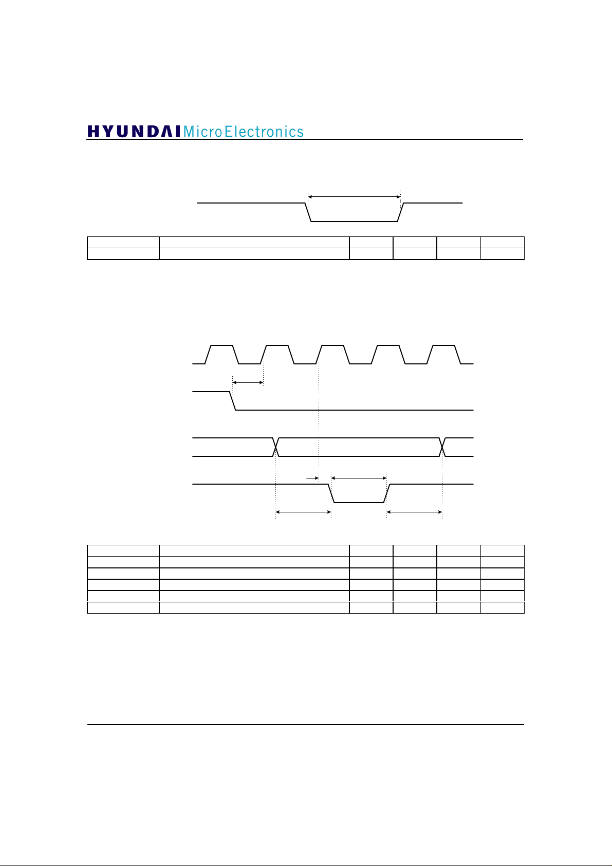
7.4.3 Reset Signal Requirement
t
RSTw
\RESET
PARAMETER PARAMETER MIN TYP MAX UNIT
tRSTw RESET pulse width tCLOCKp
The low pulse width of reset signal should be larger than tCLCOKp, the operating clock period.
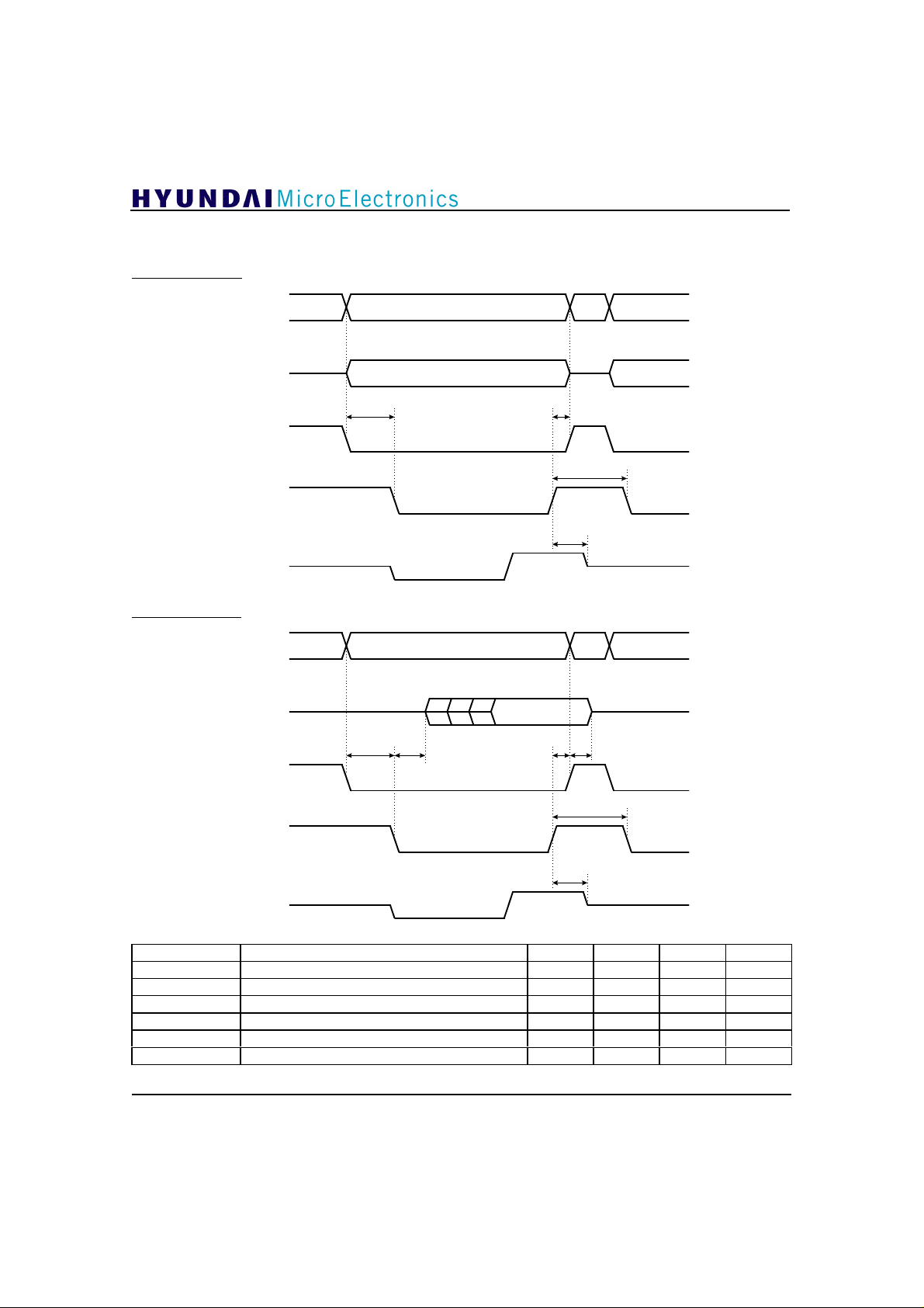
7.4.4 Audio/Video/Data Decoder Interface Requirements
CLOCK
t
REQs
VID_REQ
AUD_REQ
DATA_REQ
- -
ns
VAD_DATA[7:0]
t
STRBdtSTRBw
VID_STRB
AUD_STRB
DATA_STRB
t
VADs
t
VADh
PARAMETER PARAMETER MIN TYP MAX UNIT
tVADs VAD data setup time 30 - - ns
tVADh VAD data hold time 30 - - ns
tSTRBd STRB to clock delay time - - 18 ns
tSTRBw STRB pulse width 30 - - ns
tREQs REQ setup time 5 - - ns
32
Page 32
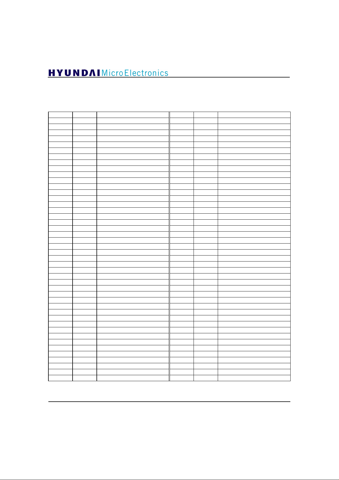
7.4.5 Host Processor Interface Requirements
Host Write Mode
DSP_ADDR[22:0]
\DSP_PD
DSP_DATA[15:0]
GDC21D301A
DSP_RWB
\DSP_STRB
DSP_READY
Host Read Mode
DSP_ADDR[22:0]
\DSP_PD
DSP_DATA[15:0]
DSP_RWB
\DSP_STRB
t
Hs
t
t
Hs
HDOE
t
Hh
t
SP
t
HRh
t
t
Hh
HDh
t
SP
t
HRh
DSP_READY
PARAMETER PARAMETER MIN TYP MAX UNIT
tHs Host setup time 0 - - ns
tHh Host hold time 0 - - ns
tHRh HREADY hold time - - 37 ns
tHDOE Host data output enabled 0 - - ns
tHDh Host data hold time 2 - - ns
tSP Strobe precharge time 37 - - ns
33
Page 33
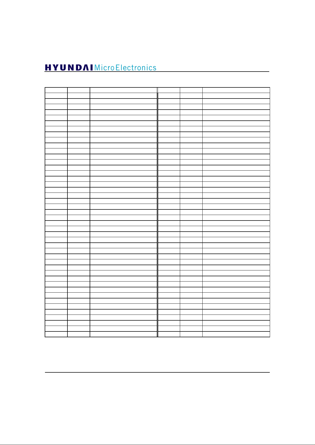
8. Package Mechanical Data
PIN
TYPE
NAME
PIN
TYPE
NAME
1
I/O
DSP_DATA[13]
45ISCAN_TEST
2
I/O
DSP_DATA[14]
46ISCAN_IN1 / TA[9]
3
I/O
DSP_DATA[15]
47IM164GND
VSS48PWR
VDD5O
DSP_INT
49ODRAM_RWB
6ODSP_READY
50ODRAM_ROW_COL_ADDR[9]
7
PWR
VDD51O
DRAM_ROW_COL_ADDR[8]
8OTDO052O
DRAM_ROW_COL_ADDR[7]
9OTDO153GND
VSS10PWR
VDD54O
DRAM_ROW_COL_ADDR[6]
11
O
HSDEN55O
DRAM_ROW_COL_ADDR[5]
12
O
HIGH_SP_DATA[1]
56ODRAM_ROW_COL_ADDR[4]
13
O
HIGH_SP_DATA[0]
57ODRAM_ROW_COL_ADDR[3]
14
O
CLOCK_OUT
58
PWR
VDD15GND
VSS59O
DRAM_ROW_COL_ADDR[2]
16
I
TA[7]60O
DRAM_ROW_COL_ADDR[1]
17
I
TA[6]61O
DRAM_ROW_COL_ADDR[0]
18
I
TA[5]62O
\DRAM_RAS1
19
I
TA[4]63GND
VSS20I
TA[3]64O
\DRAM_RAS0
21
I
TA[2]65O
\DRAM_CAS1
22
I
TA[1]66O
\DRAM_CAS0
23
I
TA[0]67I/O
DRAM_DATA[15]
24
GND
VSS68PWR
VDD25I
TWEB69I
CLOCK_27M
26
I
TEST70PWR
VDD27I
TDI71-NC28
I
P_S_MODE
72
GND
VSS29I
F_START
73
I/O
DRAM_DATA[14]
30
I
FEC_DATA[7]
74
I/O
DRAM_DATA[13]
31
I
FEC_DATA[6]
75
I/O
DRAM_DATA[12]
32
I
FEC_CLOCK
76
I/O
DRAM_DATA[11]
33
PWR
VDD77GND
VSS34-NC78
I/O
DRAM_DATA[10]
35
GND
VSS79I/O
DRAM_DATA[9]
36
I
FEC_DATA[5]
80
I/O
DRAM_DATA[8]
37
I
FEC_DATA[4]
81
I/O
DRAM_DATA[7]
38
I
FEC_DATA[3]
82
PWR
VDD39I
FEC_DATA[2]
83
I/O
DRAM_DATA[6]
40
I
FEC_DATA[1]
84
I/O
DRAM_DATA[5]
41
I
FEC_DATA[0]
85
I/O
DRAM_DATA[4]
42
I
\ERR_BLOCK
86
I/O
DRAM_DATA[3]
43
I
D_VALID
87
GND
VSS44I
SCAN_MODE / TA[8]
88
I/O
DRAM_DATA[2]
8.1 Package Pin out
GDC21D301A
34
Page 34
Package Pin out (continued)
PIN
TYPE
NAME
PIN
TYPE
NAME
89
I/O
DRAM_DATA[1]
133
I
DSP_ADDR[22]
90
I/O
DRAM_DATA[0]
134
I
DSP_ADDR[21]
91
I
\DATA_WAIT
135
I
DSP_ADDR[20]
92
I
\DATA_REQ
136
I
DSP_ADDR[19]
93
I
\AUD_WAIT
137
I
DSP_ADDR[18]
94
I
\AUD_REQ
138
I
DSP_ADDR[17]
95
I
\VID_WAIT
139
I
DSP_ADDR[16]
96
I
\VID_REQ
140
I
DSP_ADDR[15]
97
I
BOF_D
141
I
DSP_ADDR[14]
98
I
BOF_A
142
I
DSP_ADDR[13]
99
I
BOF_V
143
I
DSP_ADDR[12]
100
PWR
VDD
144
I
DSP_ADDR[11]
101
O
APWM
145
I
DSP_ADDR[10]
102
GND
VSS
146
I
DSP_ADDR[9]
103
O
\AUD_DCS
147
I
DSP_ADDR[8]
104
O
AUD_SER_DATA
148
I
DSP_ADDR[7]
105
O
\AUD_STRB
149
I
DSP_ADDR[6]
106
GND
VSS
150
I
DSP_ADDR[5]
107
O
\DATA_DCS
151
I
DSP_ADDR[4]
108
O
\DATA_STRB
152
I
DSP_ADDR[3]
109
O
PTS_DTS_STRB
153
I
DSP_ADDR[2]
110
I/O
VAD_DATA[7]
154
I
DSP_ADDR[1]
111
O
SCAN_OUT1
155
I
DSP_ADDR [0]
112
I
\RESET
156
I
BIT8MODE
113
PWR
VDD
157
I
CLOCK
114
I/O
VAD_DATA[6]
158
PWR
VDD
115
I/O
VAD_DATA[5]
159
-
NC
116
I/O
VAD_DATA[4]
160
GND
VSS
117
I/O
VAD_DATA[3]
161
I/O
DSP_DATA[0]
118
GND
VSS
162
I/O
DSP_DATA[1]
119
I/O
VAD_DATA[2]
163
I/O
DSP_DATA[2]
120
I/O
VAD_DATA[1]
164
I/O
DSP_DATA[3]
121
PWR
VDD
165
PWR
VDD
122
I/O
VAD_DATA[0]
166
I/O
DSP_DATA[4]
123
O
\VID_DCS
167
I/O
DSP_DATA[5]
124
PWR
VDD
168
I/O
DSP_DATA[6]
125
O
\VID_STRB
169
I/O
DSP_DATA[7]
126
O
VPWM
170
GND
VSS
127
I
\DSP_STRB
171
I/O
DSP_DATA[8]
128
I
DSP_RWB
172
I/O
DSP_DATA[9]
129
I
\DSP_PD
173
I/O
DSP_DATA[10]
130
GND
VSS
174
I/O
DSP_DATA[11]
131
-NC175
PWR
VDD
132
-NC176
I/O
DSP_DATA[12]
GDC21D301A
35
Page 35
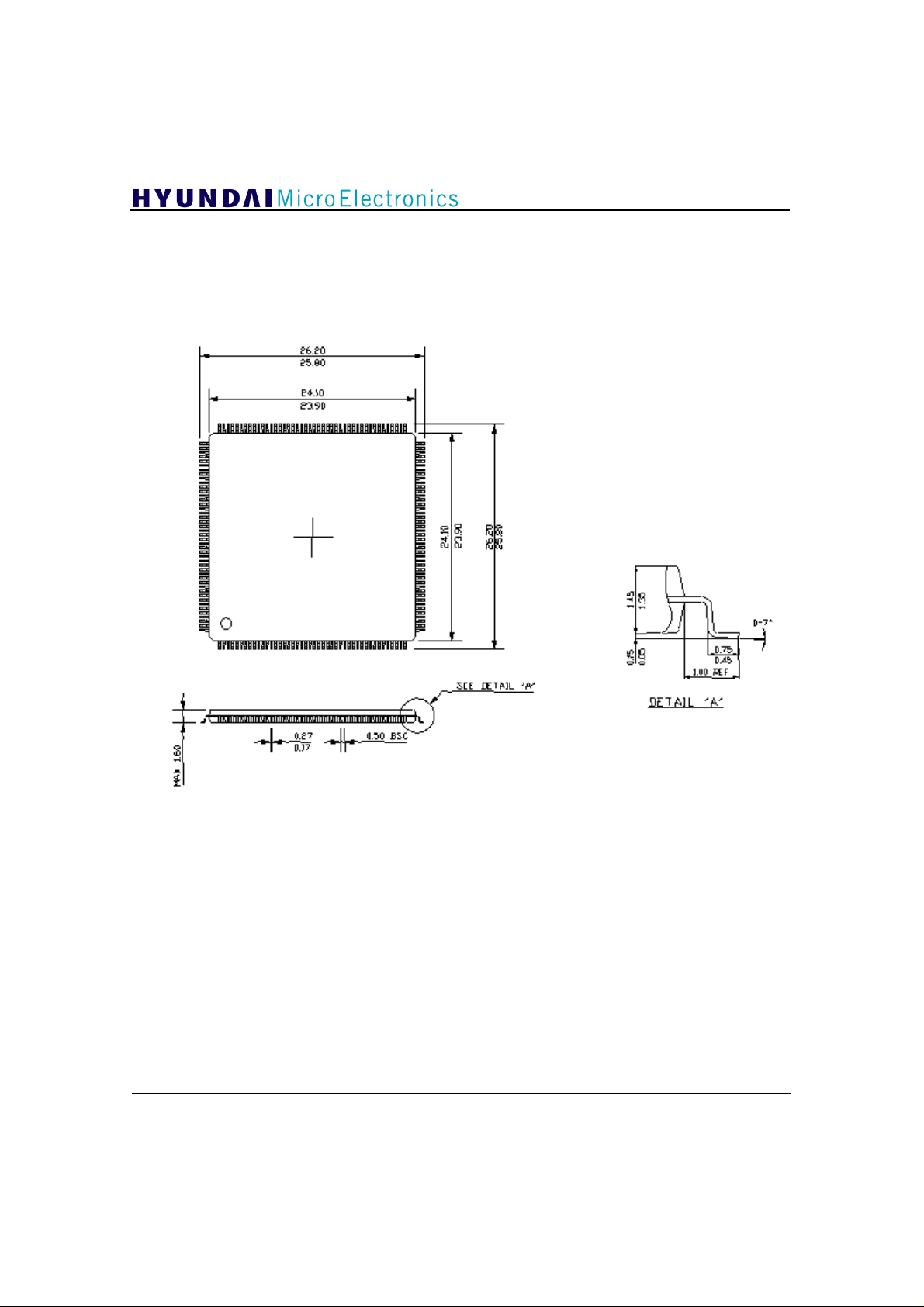
8.2 Package Dimensions
Package Type : 176 Pin Thin Quad Flat Package
24x24 mm BODY, 1.4 mm THICK
GDC21D301A
36
Figure 4. Physical Dimensions
 Loading...