

Page 1

GDC21D003
(VSB Receiver)
Version 1.0
Mar, 99
HDS-GDC21D003-9908 / 10
Page 2

GDC21D003
The information contained herein is subject to change without notice.
The information contained herein is presented only as a guide for the applications of our products. No
responsibility is assumed by Hyundai for any infringements of patents or other rights of the third parties
which may result from its use. No license is granted by implication or otherwise under any patent or
patent rights of Hyundai or others.
These Hyundai products are intended for usage in general electronic equipment (office equipment,
communication equipment, measuring equipment, domestic electrification, etc.).
Please make sure that you consult with us before you use these Hyundai products in equipment which
require high quality and / or reliability, and in equipment which could have major impact to the welfare of
human life (atomic energy control, airplane, spaceship, traffic signal, combustion control, all types of
safety devices, etc.). Hyundai cannot accept liability to any damage which may occur in case these
Hyundai products were used in the mentioned equipment without prior consultation with Hyundai.
Copyright 1999 Hyundai Micro Electronics Co.,Ltd.
All Rights Reserved
3
Page 3

GDC21D003
TABLE OF CONTENTS
1. General Description.................................................................................................................8
2. Features....................................................................................................................................8
3. Internal Block Diagram..........................................................................................................11
4. Pin Description.......................................................................................................................11
4.1 Pin Configuration ..............................................................................................................11
4.2 Pin Description..................................................................................................................14
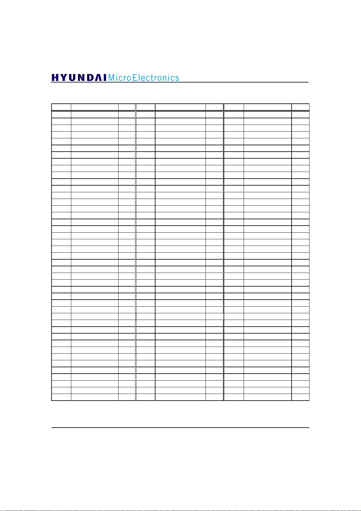
4.3 Pin Assignment.................................................................................................................16
5. I2C Bus I/F & Registers..........................................................................................................17
5.1 I2C Bus I/F Description......................................................................................................17
5.1.1 Write Operation...........................................................................................................17
5.1.2 Read Operation...........................................................................................................17
5.2 I2C Bus Register Configuration.........................................................................................18
5.3 I2C Bus Register Description ............................................................................................20
6. Functional Description..........................................................................................................29
6.1 ADC ..................................................................................................................................29
6.1.1 Electrical Characteristics.............................................................................................30
6.1.2 Timing Diagram...........................................................................................................32
6.1.3 Application Circuits......................................................................................................33
6.2 Clock Divider.....................................................................................................................35
6.3 Synchronizer.....................................................................................................................36
6.3.1 Input Control................................................................................................................36
6.3.2 DC Reduction..............................................................................................................39
6.3.3 Auto Gain Control(AGC) .............................................................................................39
6.3.4 Polarity Correction.......................................................................................................40
6.3.5 Data Segment Sync Recovery....................................................................................41
6.3.6 Polarity Decision..........................................................................................................42
6.3.7 Timing Recovery .........................................................................................................43
6.3.8 Field Sync Recovery...................................................................................................46
6.3.9 VSB Mode Detect........................................................................................................47
6.3.10 NTSC Rejection.........................................................................................................48
6.4 Equalizer...........................................................................................................................50
6.4.1 Block Diagram.............................................................................................................50
6.4.2 Training/Data Mode Equalization................................................................................51
6.4.3 Error Estimation...........................................................................................................52
6.4.4 Adaptive Filter .............................................................................................................53
6.4.5 Equalizer Clock Scheme.............................................................................................53
6.4.6 I2C Bus I/F...................................................................................................................54
6.4.7 Coefficient Reading/Writing.........................................................................................56
4
Page 4

GDC21D003
6.5 Phase Tracker ..................................................................................................................56
6.5.1 Error Detection............................................................................................................57
6.5.2 Gain & Offset Loop......................................................................................................58
6.5.3 Phase Loop.................................................................................................................58
6.5.4 I2C Bus I/F ..................................................................................................................59
6.6 Channel Decoder..............................................................................................................60
6.6.1 12 Symbol Intrasegment Deinterleaver.......................................................................61
6.6.2 Segment Sync Suspension.........................................................................................61
6.6.3 Viterbi Decoder............................................................................................................62
6.6.4 Symbol-to-Byte Converter...........................................................................................64
6.6.5 Convolutional Deinterleaver........................................................................................65
6.6.6 Reed-Solomon Decoder..............................................................................................65
6.6.7 Data Derandomizer.....................................................................................................66
6.6.8 I/F to Transport Demultiplexer.....................................................................................67
6.7 PLL....................................................................................................................................74
7. Electrical Characteristics......................................................................................................75
8. Package Dimensions.............................................................................................................77
9. Application Notes ..................................................................................................................78
Figures
Figure 3.1 Functional Block Diagram ..............................................................................10
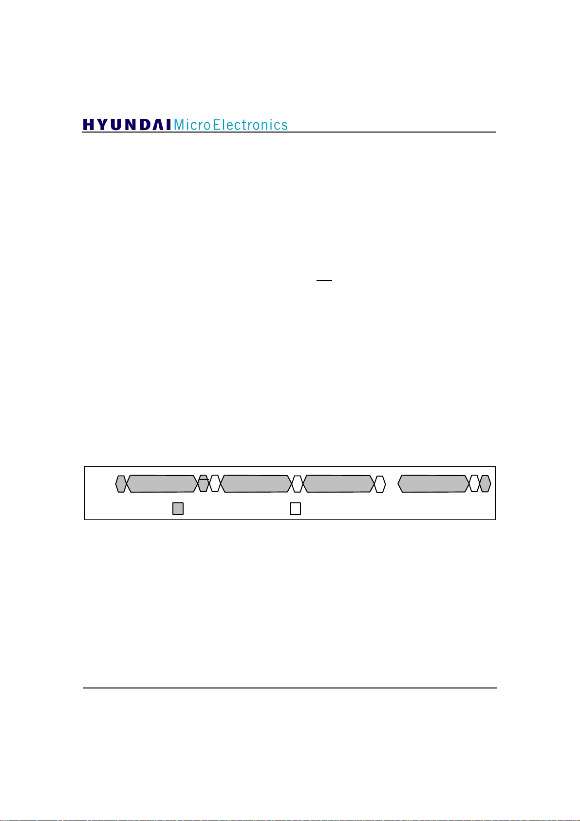
Figure 5.1.1 I2C Write Operation Example ..........................................................................17
Figure 5.1.2 I2C Read Operation Example ..........................................................................18
Figure 6.1.1 The Block Diagram of ADC .............................................................................29
Figure 6.1.2 Timing Diagram of ADC ..................................................................................32
Figure 6.1.3 ADC Application Circuit ...................................................................................33
Figure 6.1.4 Equivalent Circuits ..........................................................................................34
Figure 6.3.1 The Block Diagram of Input Selection ............................................................36
Figure 6.3.2 Digital Input Setting Up & Chip I/F Circuit(1) ..................................................37
Figure 6.3.3 Digital Input Setting Up & Chip I/F Circuit(2) ..................................................38
Figure 6.3.4 The Block Diagram of DC Reduction ..............................................................39
Figure 6.3.5 The Block Diagram of AGC ............................................................................40
Figure 6.3.6 AGC Signal I/F for DTV System .....................................................................40
Figure 6.3.7 The Block Diagram of Polarity Correction .......................................................41
Figure 6.3.8 The Block Diagram of Data Segment Sync Recovery ....................................41
Figure 6.3.9 Polarity signal I/F Circuit .................................................................................42
Figure 6.3.10 Timing Recovery Block ....................................................................................43
Figure 6.3.11 Timing Recovery I/F Circuit(1) .........................................................................44
Figure 6.3.12 Timing Recovery I/F Circuit(2) .........................................................................45
Figure 6.3.13 Field Sync Structure ........................................................................................46
Figure 6.3.14 The Block Diagram of Field Sync Recovery ....................................................46
Figure 6.3.15 Comb Filter Block ............................................................................................48
5
Page 5

GDC21D003
Figure 6.3.16 The Block Diagram of NTSC Rejection............................................................49
Figure 6.4.1 Channel Equalizer ...........................................................................................50
Figure 6.4.2 VSB Slicer .......................................................................................................51
Figure 6.4.3 Training/Data Equalization ..............................................................................51
Figure 6.4.4 VSB Slice Level ..............................................................................................52
Figure 6.4.5 Coefficient Update Filter .................................................................................53
Figure 6.4.6 I2C Bus I/F .......................................................................................................54
Figure 6.5.1 Phase Tracker .................................................................................................57
Figure 6.5.2 Error Detection ................................................................................................57
Figure 6.5.3 Coefficients of Hilbert Transform Filter ...........................................................58
Figure 6.5.4 Complex Multiplier ..........................................................................................58
Figure 6.6.1 Block Diagram of Channel Decoder ...............................................................60
Figure 6.6.2 12-Symbol Intrasegment Deinterleaver ..........................................................61
Figure 6.6.3 Segment Sync Suspension .............................................................................62
Figure 6.6.4 Viterbi Decoding with and without NTSC Rejection Filter ...............................63
Figure 6.6.5 Internal Block Diagram of Viterbi Decoder ......................................................63
Figure 6.6.6 Convolutional Deinterleaver ............................................................................65
Figure 6.6.7 Derandomizer Polynomial ...............................................................................66
Figure 6.6.8 I/F to Transport Demultiplexer when Register64[7:0] is set to
Default Value ....................................................................................................68
Figure 6.6.9 I/F to Transport Demultiplexer when Register64[3] (Derand_on)
is set to ‘ 0’ ........................................................................................................69
Figure 6.6.10 I/F to Transport Demultiplexer when Register64[2](Errorflg_ins)
is set to ‘ 0’ ........................................................................................................69
Figure 6.6.11 I/F to Transport Demultiplexer when Register64[1](Vsbdvalid_pol)
is set to ‘ 0’ ........................................................................................................70
Figure 6.6.12 I/F to Transport Demultiplexer when Register64[0](Vsbclk_sup)
is set to ‘ 0’ ........................................................................................................70
Figure 6.6.13 I/F to Transport Demultiplexer(MMDS 8VSB Mode) .......................................71
Figure 6.6.14 I/F to Transport Demultiplexer at Serial Output Mode .....................................71
Figure 6.6.15 Connection with VSB Receiver and Transport Demultiplexer
Chip(GDC21D301A) ........................................................................................72
Figure 6.6.16 Connection with VSB Receiver and Transport Demultiplexer
Chip(L64007) ...................................................................................................72
Figure 6.6.17 Connection with VSB Receiver and Transport Demultiplexer
Chip(AVIA-MAX) ..............................................................................................73
Figure 6.7.1 Clock Scheme .................................................................................................74
Figure 7.1 Clock Reset Stabilization Timing .....................................................................76
Figure 7.2 Input and Output Timing ..................................................................................76
Figure 8.1 Physical Dimensions ........................................................................................77
Figure 9.1 VSB Receiver Application Circuit .....................................................................78
6
Page 6

GDC21D003
Tables
Table 6.2.1 Register Setting Up for Clock Divider .............................................................35
Table 6.3.1 Input Signal Path Setting Up ..........................................................................36
Table 6.3.2 DATAPOLP & DATAPOLN Output ................................................................42
Table 6.3.3 VSB Mode Data for Each VSB Mode .............................................................47
Table 6.3.4 VSB Mode Signal Control ..............................................................................47
Table 6.3.5 Comb Filter Control through I2C Bus ..............................................................49
Table 6.4.1 Contents of I2C Bus Register33 for Equalizer ................................................55
Table 6.4.2 Contents of I2C Bus Register33 for Filter Control ..........................................55
Table 6.5.1 Contents of I2C Bus Register33 for Phase Tracker ........................................59
Table 6.5.2 Contents of I2C Bus Register33 for Gain Control ...........................................59
Table 6.6.1 Bypassed Sub-blocks by the Values of I2C Bus Register64 ..........................60
Table 6.6.2 Symbol-to-Byte Conversion ...........................................................................64
Table 6.6.3 I2C Register64 Flags controlling Transport Demultiplexer I/F ........................67
7
Page 7

GDC21D003
VSB Receiver
GDC21D003
1. General Description
The VSB Receiver(GDC21D003) is an ATSC
compliant single chip communications device that
synchronizes, equalizes, and corrects errors of
ATSC 8/16 VSB and MMDS (Multichannel
Multipoint Distribution System) 2/4/8/16 VSB
modulated signal.
The on-chip 10-bit 10.76Msps Analog-to-Digital
Converter has an input sample-and-hold amplifier.
By implementing a multistage pipelined
architecture with output correction logic, the ADC
offers accurate performance and guarantees no
missing codes over the full operating temperature.
Clock divider divides output clock of external
VCXO and generates symbol clock (CLKFS) and
ADCCLK. The CLKFS has 10.76MHz frequency
as symbol frequency used in DTV transmitter,
ADCCLK is used for external A/D converter. At
this time, if you use digital signal as input of chip,
CLKFS or ADCCLK are used for external A/D
converter clock.
Synchronizer removes DC entered from transmitter
and DC generated by analog circuit used in
receiver. Also it checks gain of input signal and
sends it to demodulator, detects polarity, and
corrects it. It recovers Data Segment Sync period
and Field Sync period entered from transmitter. It
detects VSB mode of current input signal and
removes NTSC co-channel interference in channel.
Equalizer corrects linear distortion created during
transmission. It uses Least-Mean-Square algorithm
and has decision feedback equalizer structure. It
uses adaptive filter having coefficient update
structure consisted of multiplier, adder, and
memory structure in every tap.
Phase Tracker compensates phase distortion due to
phase noise and it consists of gain correction loop
for gain error, offset correction loop for offset error,
and phase correction loop for phase error.
Channel Decoder consists of Viterbi Decoder,
Convolutional Deinterleaver, Reed-Solomon
Decoder, Data Derandomizer, and etc. It decodes
ATSC 8/16 VSB signal and MMDS 2/4/8/16 VSB
signal. Also it has internal segment error counter
that send out the number of segment errors per
second and offers tri-state parallel/serial Transport
Demultiplexer interface.
2. Features
General features
• ATSC compliant 8/16 VSB receiver
• MMDS 2/4/8/16 VSB receiver
• SNR threshold 14.9 dB on AWGN channel
• Tri-state parallel/serial MPEG-2 transport
interface
• Supports I2C bus interface
• Boundary Scan Test circuit complies with
IEEE Std. 1149.1
ID-Code = 0D0031C1
• Operating voltage : 3.3V
• 0.35µm CMOS technology
• 128 pin HQFP package
ADC
• Resolution : 10bits (≤ ±1⁄2 LSB DNL error)
• Sampling rate : 10.76 Msps
• Differential input range : 2Vpp(1.7 ± 0.5V
differential)
Clock Divider
• Generates symbol clock(10.76MHz)
• Uses one of two VCXOs, fs(10.76MHz) and
2fs(21.52MHz) as input
Synchronizer
• Input control
• DC reduction and polarity correction
- Correction of polarity ambiguity caused
by FPLL
• Non-coherent and coherent automatic gain
control (AGC)
• Data Segment Sync and Field Sync recovery
• Timing recovery
• Polarity decision
- Polarity decision after Data Segment
Sync is locked
• VSB mode detection
• Comb control
- Comb filter for the rejection of NTSC
co-channel interface
8
Page 8

Equalizer
• Decision feedback equalizer
• Supports training sequence and blind
equalization
• Concurrent coefficients update in symbol
time
• Available 3 different step-size
• Capability of reading equalizer coefficients
• Ghost cancellation in the range from -2.86µs
to 20.76µs
Phase Tracker
• Intelligent loop control according to noise
environment
• Phase tracking from -60° to 60° with
resolution of 0.004 degree
• Phase, offset, and gain correction at a time
Channel Decoder
• Concatenated Viterbi/Reed-Solomon Decoder
with Deinterleaver and Derandomizer
• Internal segment error counter
• Tri-state parallel/serial MPEG-2 Transport
Demultiplexer interface
GDC21D003
9
Page 9
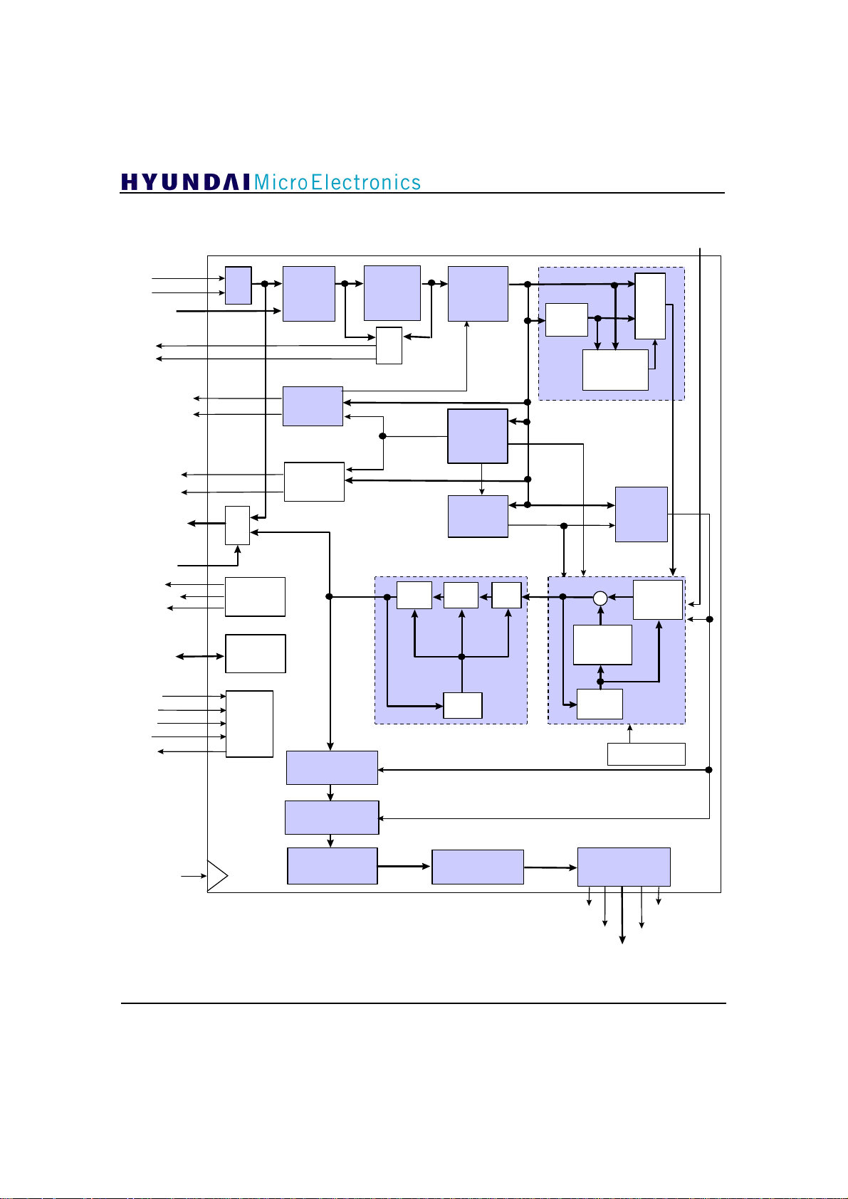
3. Internal Block Diagram
GDC21D003
NADTONDATA
INN
INP
DIN[9:0]
GUP
GDN
DATAPOLP
DATAPOLN
NCHGUP
NCHGDN
DOUT[9:0]
TM[2:0]
VCXO
ADCCLK
CLKFS
I2C BUS
ADC
Mux
Clock
Divider
I2C
Interface
Input
SelectionDCReduction
AGC
Polarity
Decision
Timing
Recovery
Phase
Loop
Polarity
Correction
Data
Segment
Sync
Recovery
Field
Sync
Recovery
Offset
Loop
Gain
Loop
Comb
Filter
Comparator
NTSC Rejection
Σ
192 Tap
Feedback
Filter
Mux
MSE
&
VSB
Mode
Detect
64 Tap
Forward
Filter
TRST
TMS
TCK
TDI
TDO
SYMCLK
10
JTAG
Error
Detect
Phase Tracker
Deinterleaver/
Viterbi Decoder
Convolutional
Deinterleaver
Reed-Solomon
Decoder
Data
Derandomizer
Figure 3.1 Functional Block Diagram
Error
Control
Equalizer
Transport
Demultiplexer I/F
VSBCLK
VSBDVALID
VSBDATA[7:0]
4x Clock
4X PLL
VSBSOP
NVSBERRFLG
Page 10
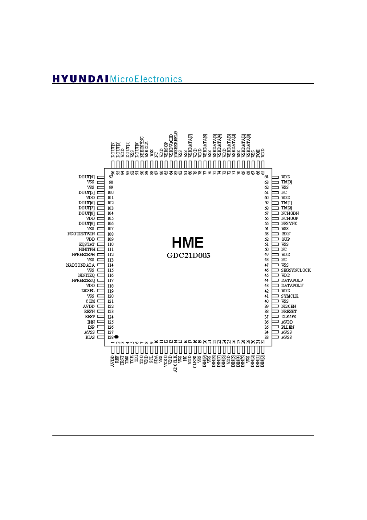
4. Pin Description
4.1 Pin Configuration
GDC21D003
∗
128 PIN HQFP, 28X28 mm BODY, 1.60/0.33 mm FORM, 3.37mm THICK, 0.8 mm PITCH
11
Page 11
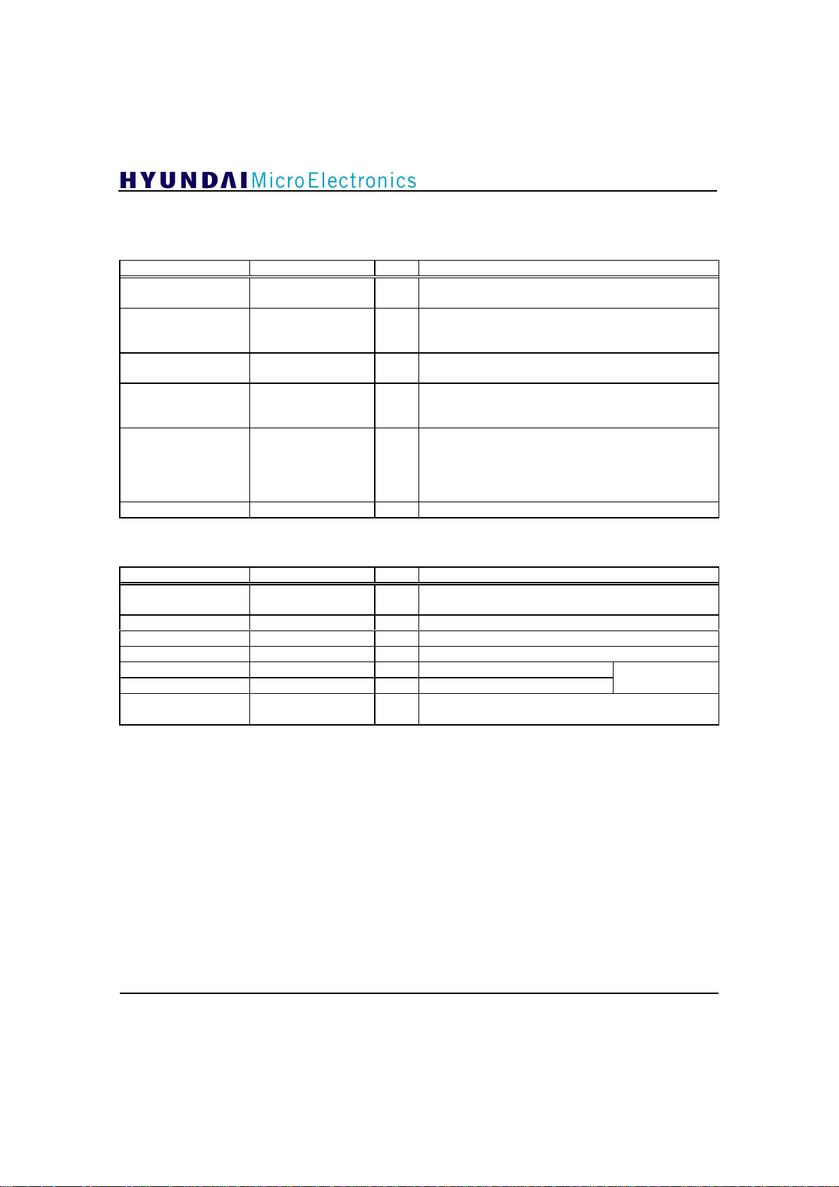
4.2 Pin Description
Clock/Reset ; 6 Pins
PIN NAME TYPE DESCRIPTION
38
12
14
18
37
41
A/D Converters ; 7 Pins
PIN NAME TYPE DESCRIPTION
2
121
123
124
125
126
128
NRESET I
VCXO I
ADCCLK O Clock for Off-chip ADC(21.52MHz or 10.76MHz);
CLKFS O
CLK4FS I/O Test clock/4x symbol clock;
SYMCLK I System clock input(10.76MHz)
REF I
COM I Common voltage(1.5V)
REFN I Reference voltage(bottom: 1.2V)
REFP I Reference voltage(top: 2.2V)
INN I Analog data input(negative)
INP I Analog data input(positive)
BIAS I
GDC21D003
System reset(active low); This signal should be
activated on channel change or power on.
Clock input generated in VCXO; This pin can be
connected to one of two VCXOs whose output
frequencies are fs(10.76MHz) and 2fs(21.52MHz).
This clock is generated by dividing VCXO input signal.
System clock; This clock is generated from dividing
VCXO input signal. Its frequency is the same of symbol
rate(10.76MHz).
When PLLEN(pin35) input is set to ‘1’, this pin is used
as 4x symbol clock output.
When PLLEN(pin35) input is set to ‘0’, this pin is used
as test clock(43.04MHz) input.
Bias register for internal ADC; This pin should be
connected to AVDD(3.3V) via 12k ohm register.
1.65 ± 0.5V
differential
Bias input(2V typical) for On-chip ADC; This pin
should be connected to AVSS via 0.1µF capacitor.
12
Page 12
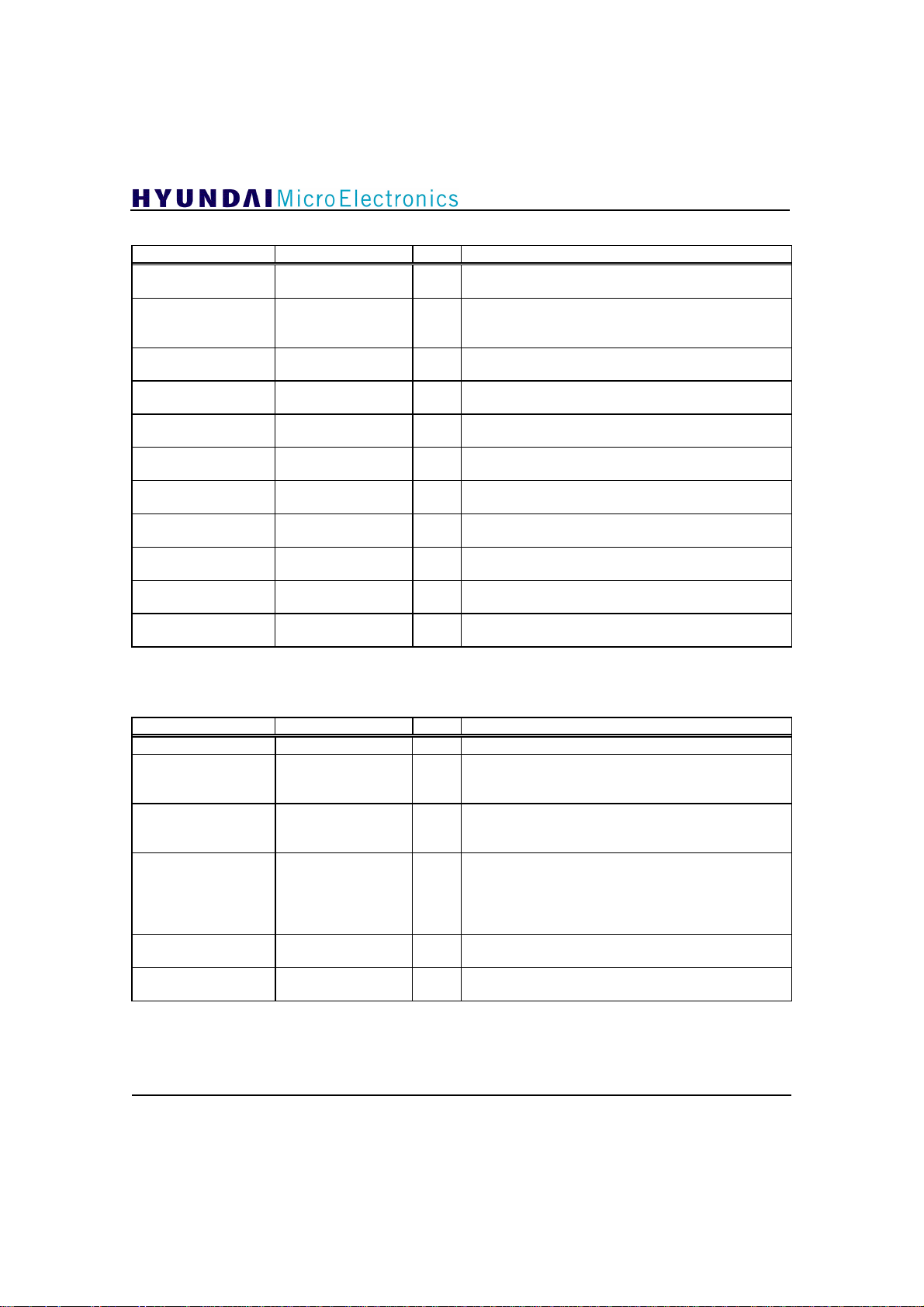
GDC21D003
Sync Recovery ; 20 Pins
PIN NAME TYPE DESCRIPTION
20, 22-24, 26-28,
30-32
44
43
46
52
53
55
56
57
66
90
(NOTE) * These five I/O pins are used as input pin only for chip test.
DIN[9:0]
Bit9 : MSB
DATAPOLP I/O
DATAPOLN I/O*Inverted polarity signal of input data(active high);
SEGSYNCLOCK I/O*Stability Indication of Data Segment Sync
GUP I/O
GDN I/O
NFSYNC O
NCHGUP O Charging signal for charge pump in the timing
NCHGDN O Discharging signal for charge pump in the timing
FOE O
NSEGSYNC O
Equalizer ; 6 Pins
PIN NAME TYPE DESCRIPTION
35
108
110
114
116
117
(NOTE) When I2C is enabled, operation is performed either using these pins or via I2C register, but
when disabled, only these pins are used. If you want to control Equalizer fast, use these external
input pins. Otherwise use I2C bus registers.
PLLEN I
NCOUPDTWIN O
EQSTAT O
NADTONDATA I Data mode coefficient update(active low);
NINITEQ I
NFREEZEEQ I
Digital data input; This data input comes from
I
external ADC.
*
Polarity signal of input data(active high); If this
output value is ‘1’, it means the plus polarity.
This signal should be applied to demodulator IC.
This signal should be applied to demodulator IC.
recovery(active high)
*
Input data gain increasing signal(active high); This
signal should be applied to demodulator IC.
*
Input data gain decreasing signal(active high); This
signal should be applied to demodulator IC.
Field Sync(active low); If this output value is ‘0’, it
means Field Sync interval.
recovery block(active low)
recovery block(active low)
Field status indicator(active high); If this output value
is ‘1’, it means inverted field.
Data Segment Sync(active low); If this output value is
‘0’, it means Data Segment Sync interval.
PLL enable(active high); This pin should be set to ‘1’.
Coefficient update window(active low); If this output
value is ‘0’, the Equalizer adapts its coefficients.
Otherwise, it doesn't adapt its coefficients.
Equalizer status; If this output value is ‘1’, the
Equalizer is in normal status.
Otherwise, the Equalizer has diverged.
If this input is set to ‘0’, the Equalizer adapts its
coefficients during training sequence and data interval.
Otherwise, the Equalizer adapts its coefficients during
only training sequence interval.
Equalizer initialization(active low); If this input is set
to ‘0’, the Equalizer is initialized.
Equalizer freeze(active low); If this input is set to ‘0’,
the Equalizer coefficient does not be adapted.
13
Page 13
GDC21D003
Phase Tracker ; 2 Pins
PIN NAME TYPE DESCRIPTION
111
112
(NOTE) When I2C is enabled, operation is performed either using these pins or via I2C register, but
when disabled, only these pins are used. If you want to control Equalizer fast, use these
external input pins. Otherwise use I2C bus registers.
NINITPH I
NFREEZEPH I
Channel Decoder ; 12 Pins
PIN NAME TYPE DESCRIPTION
68,69,71,72,74,75,77,
80
83
84
85
89
VSBDATA[7:0]
Bit7 : MSB
NVSBERRFLG O
VSBDVALID O Valid data indication flag;
VSBSOP O Start byte indicator of a packet
VSBCLK O Data clock of packet data
Phase tracker initialization(active low); If this input
is set to ‘0’, the Phase Tracker is initialized.
Phase tracker freeze(active low) ; If this input is set to
‘0’, the Phase Tracker stops phase tracking..
O Data output to transport multiplexer;
VSBDATA[7] : Used as start bit indicator of a byte in
serial output mode.
VSBDATA[0] : Used as serial data output in serial
output mode.
Packet error indication flag(active low); This output
indicates whether the packet has error or not.
0 : with error
1 : without error
1: valid when register64[1](Vsbdvalid_pol = ‘1’)
0 :valid when register64[1](Vsbdvalid_pol = ‘0’)
I2C Bus Interface ; 4 Pins
PIN NAME TYPE DESCRIPTION
9
10
39
119
SCL I I2C bus serial clock input
SDA I/O I2C bus serial data input/output
NI2CEN I
I2CSEL I I2C bus device address selection;
Boundary Scan Signal ; 5 Pins
PIN NAME TYPE DESCRIPTION
3
4
5
6
7
TRST I Boundary scan test reset
TMS I Boundary scan test mode selection
TCK I Boundary scan test clock
TDI I Boundary scan test data input
TDO O Boundary scan test data output
14
2
I
C bus enable(active low); If this input is set to ‘0’,
the chip is controlled by I2C bus.
Otherwise, stand alone mode.
2
0 : I
C device address is set to b"1011001".
2
1 : I
C device address is set to b"0001110".
(default value)
Page 14
Miscellaneous ; 18 Pins
PIN NAME TYPE DESCRIPTION
58,59,63
91, 93, 95-97, 100,
102-104, 106
16,48,50,61,87
TM[2:0]
Bit2 : MSB
DOUT[9:0]
Bit9 : MSB
NC No connection
Supply Voltages ; 48 Pins
PIN NAME TYPE DESCRIPTION
8, 13, 17, 25, 42, 45,
49,60,64,65,73,78,
79,86,94,101,105,
109,118
11,15,19,21,29,40,
VDD Digital positive supply voltage(3.3V)
VSS Digital negative supply voltage(ground)
47,51,54,62,67,70,
76,81,82,88,92,98
99,107,113,115
1,36,122
33,34,120,127
AVDD Analog positive supply voltage(3.3V)
AVSS Analog negative supply voltage(ground)
GDC21D003
I Tmode;
“111” : normal mode with ADC output
“011” : normal mode with Phase Tracker output
others : reserved for chip test
Data output; Either ADC or Phase Tracker block
O
output is selected by tmode as dout[9:0] output.
15
Page 15
GDC21D003
4.3 Pin Assignment
PIN NAME TYPE PIN NAME TYPE PIN NAME TYPE
1 AVDD 44 DATAPOLP I/O 87 NC
2 REF I 45 VDD 88 VSS
3 TRST I 46 SEGSYNCLOCK I/O 89 VSBCLK O
4 TMS I 47 VSS 90 NSEGSYNC O
5 TCK I 48 NC 91 DOUT[0] O
6 TDI I 49 VDD 92 VSS
7 TDO O 50 NC 93 DOUT[1] O
8 VDD 51 VSS 94 VDD
9 SCL I 52 GUP I/O 95 DOUT[2] O
10 SDA I/O 53 GDN I/O 96 DOUT[3] O
11 VSS 54 VSS 97 DOUT[4] O
12 VCXO I 55 NFSYNC O 98 VSS
13 VDD 56 NCHGUP O 99 VSS
14 ADCCLK O 57 NCHGDN O 100 DOUT[5] O
15 VSS 58 TM[2] I 101 VDD
16 NC 59 TM[1] I 102 DOUT[6] O
17 VDD 60 VDD 103 DOUT[7] O
18 CLKFS O 61 NC 104 DOUT[8] O
19 VSS 62 VSS 105 VDD
20 DIN[9] I 63 TM[0] I 106 DOUT[9] O
21 VSS 64 VDD 107 VSS
22 DIN[8] I 65 VDD 108 NCOUPDTWIN O
23 DIN[7] I 66 FOE O 109 VDD
24 DIN[6] I 67 VSS 110 EQSTAT O
25 VDD 68 VSBDATA[0] O 111 NINITPH I
26 DIN[5] I 69 VSBDATA[1] O 112 NFREEZEPH I
27 DIN[4] I 70 VSS 113 VSS
28 DIN[3] I 71 VSBDATA[2] O 114 NADTONDATA I
29 VSS 72 VSBDATA[3] O 115 VSS
30 DIN[2] I 73 VDD 116 NINITEQ I
31 DIN[1] I 74 VSBDATA[4] O 117 NFREEZEEQ I
32 DIN[0] I 75 VSBDATA[5] O 118 VDD
33 AVSS 76 VSS 119 I2CSEL I
34 AVSS 77 VSBDATA[6] O 120 AVSS
35 PLLEN I 78 VDD 121 COM I
36 AVDD 79 VDD 122 AVDD
37 CLK4FS I/O 80 VSBDATA[7] O 123 REFN I
38 NRESET I 81 VSS 124 REFP I
39 NI2CEN I 82 VSS 125 INN I
40 VSS 83 NVSBERRFLG O 126 INP I
41 SYMCLK I 84 VSBDVALID O 127 AVSS
42 VDD 85 VSBSOP O 128 BIAS I
43 DATAPOLN I/O 86 VDD
16
Page 16
GDC21D003
5. I2C Bus I/F & Registers
5.1 I2C Bus I/F Description
When NI
may be controlled over I2C bus interface which
consists of two signals, serial data(SDA) and serial
clock(SCL) that can control a large number of
devices on a common bus. The Device Address of
this chip is “1011001”b or “0001110”b which can
be selected by I2CSEL pin. The data on the I2C bus
can be transferred at a rate up to 100 kbits/s in the
standard mode, or up to 400 kbits/s in the fast
mode. In the GDC21D003, SDA is bi-directional
but SCL is only used as input, since the IC can only
act as a slave device. In normal operations, data
transfers are clocked by the SCL signal with one
SCL pulse per data bit, and SDA is required to be
stable during the high period of the SCL signal.
Transitions of SDA while SCL is high are
performed by the interface signals of start(S),
stop(P), and repeated start(Sr) conditions. The start
condition is defined as a high-to-low transition of
SDA while SCL is high, and the stop condition is
the low-to-high transition of SDA while SCL is
high. Data transmissions are always proceeded by a
start condition and ended with a stop condition, and
may contain repeated starts within the transmission
to alter the direction of the data flow or to change
register base addresses. All data transmission
2
CEN pin is set to Low, the GDC21D003
operations occur in 8-bit blocks with each block
acknowledged through the designated receiver by
the generation of an acknowledge signal(A). This
signal is generated on the ninth pulse of SCL for
each transferred block.
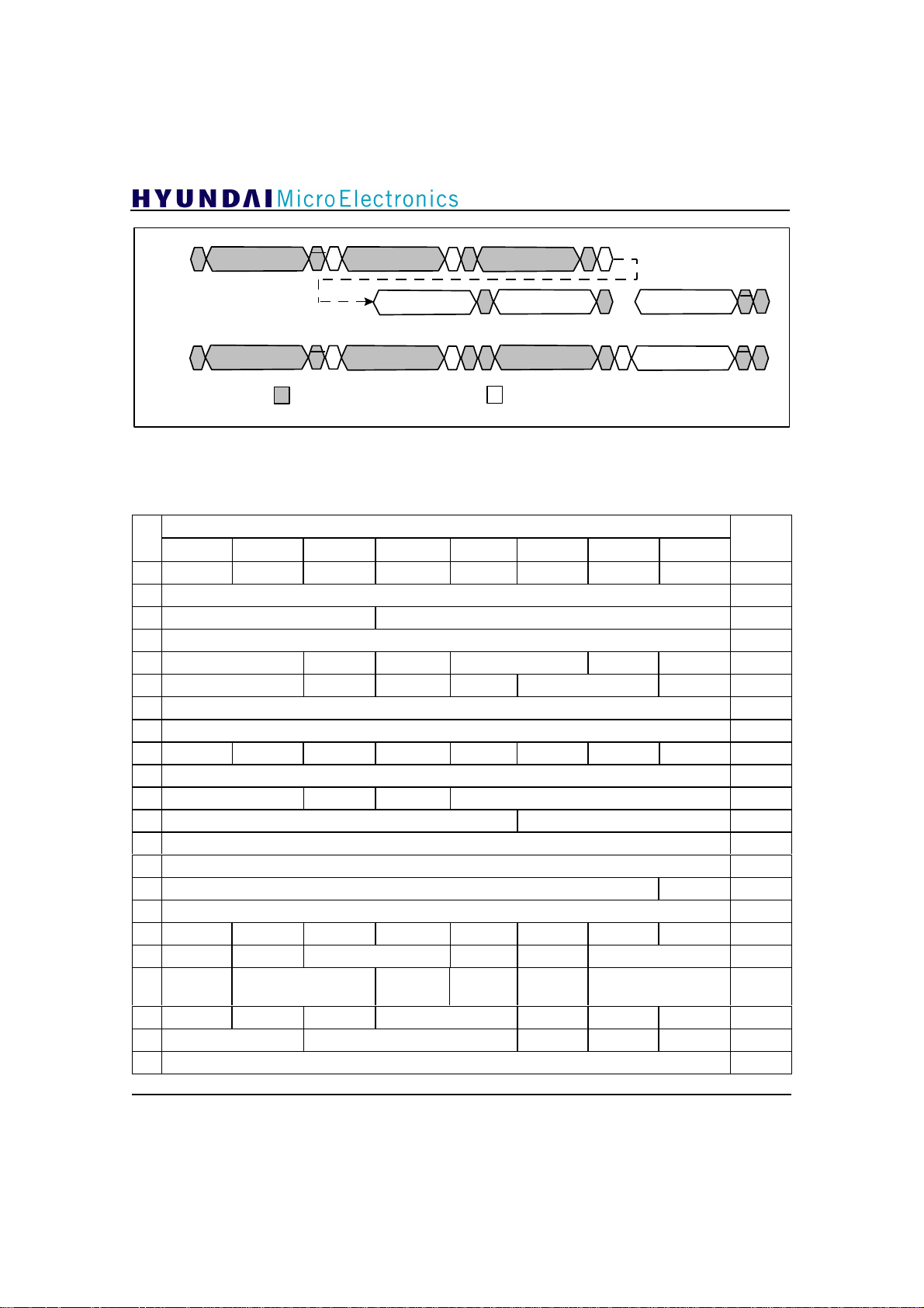
5.1.1 Write Operation
In order to perform a write operation, the interface
is accessed in following manner. The master first
generates a start condition by pulling SDA down to
low while SCL is high. The master next sends a 7bit Device Address and a one bit R/W signal, and
each slave compares this address with its own
address and acknowledges the master if the device
address sent by the master coincides with that of its
own. If not so, the slave ignores the rest of current
data being transmitted. If the master is writing to
the GDC21D003, the chip interprets the next data
byte as a register base address. This is used as the
location to store the next received data byte. This
base address increases as each data byte is received
allowing a contiguous register block to be
programmed in a single transmission. Noncontiguous blocks may be programmed in multiple
transmissions or by using a repeated start condition,
which allows a new Device Address and register
base address to be specified without the master
giving up control of the bus. The transmission is
terminated with the receipt of a stop condition.
A BASE ADDRESS A DATA #1
ISSUED BY MASTER
SDA
DEV. ADDRESS W
S
Figure 5.1.1 I
5.1.2 Read Operation
Read operation is performed in a manner similar
to write operation. The master first generates a
start condition and then sends the Device Address
and R/W signal. The master will acknowledge
each byte as receiving if it desires another byte to
be sent. At the end of the transmission, the master
will not acknowledge the slave and will then be
ISSUED BY GDC21D003
2
C Write Operation Example
free to generate a stop condition to terminate the
transmission. The base address register contents
are used to determine the location to be read, and
once again this address will be increased with each
successive read. Because the base address register
can only be programmed through a write operation,
a general read will require two accesses or a single
access with a embedded repeated start to change
the direction of transmission.
…
A
DATA #N A
P
17
Page 17
GDC21D003
A
A
A
P S DEV. ADDRESSDEV. ADDRESS
DEV. ADDRESS
DATA #2
ISSUED BY GDC21D003
ASDA SrW
R
…
A
R DATA #1
DATA #N
A
SDA
DEV. ADDRESS
S
S
A BASE ADDRESS
DATA #1
A BASE ADDRESS
W
ISSUED BY MASTER
C Read Operation Example
Figure 5.1.2 I
2
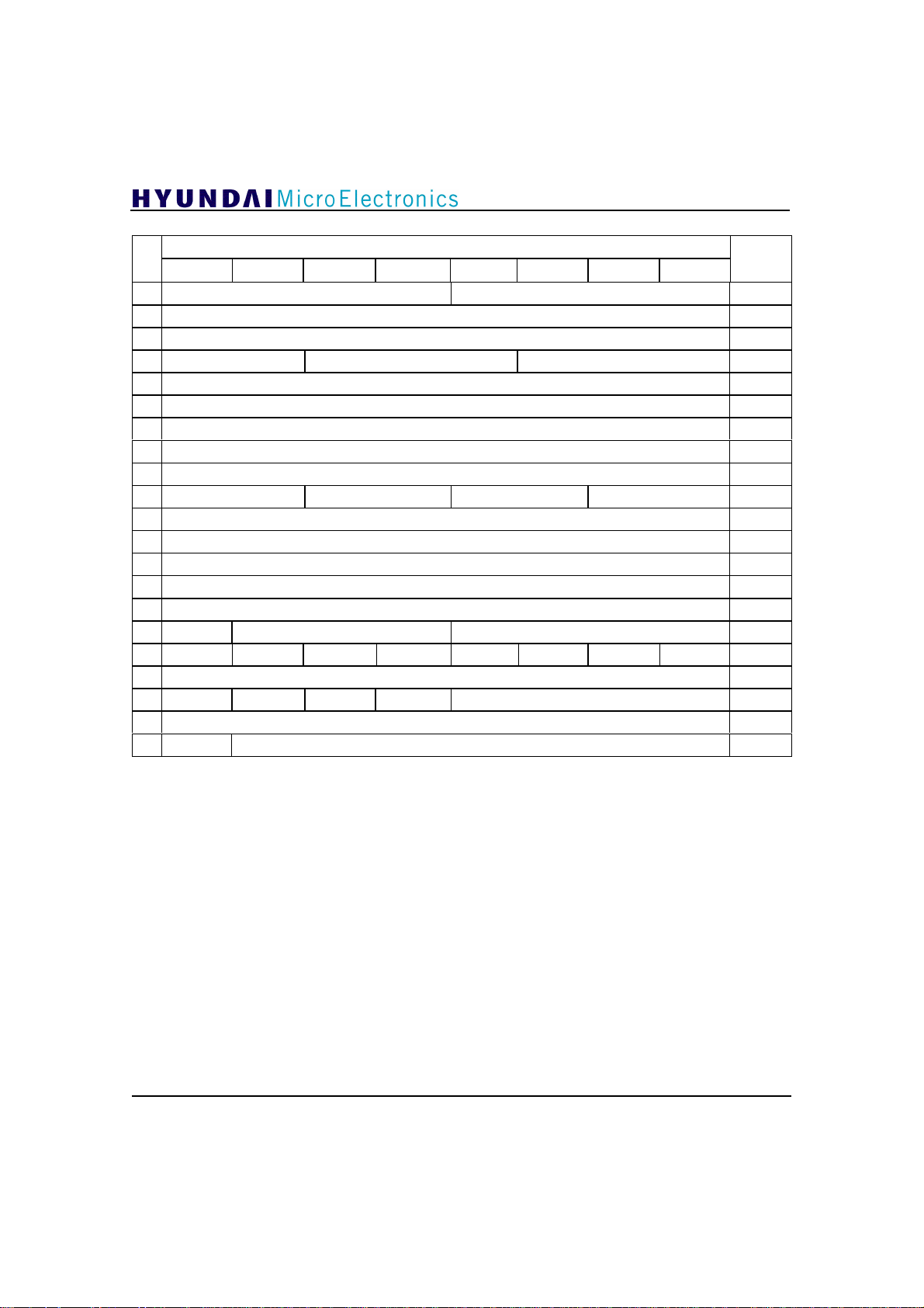
5.2 I2C Bus Register Configuration
Add
ress
0
D7 D6 D5 D4 D3 D2 D1 D0
Dinmode Dinsel ADCCLKSEL ADCCLKPH DCbypass DChold AGChold AGCoffsetW 11110000
1
2
VSBmod[2:0] “ 10010 ” 10110010
3
4
5
“ 00 “ PolarityW Polarity “ 10 “ nSyncLockrst VSBmodW 00001000
VCXOSEL[1:0] nCombW nComb Combouthalf NoCombgain[1:0] “ 0 “ 00011010
6
7
8
X nSyncLock nSegLock Combstat nVSBmodstart DATAPOLN nPolLock nFldLock
9
10
11
X nFrmLock nVSBLock “ 0101 “ XXXX0101
X VSBmodA[2:0]
12
13
14
15
nSyncLockPH U U nCombPH nSyncLockEQ nDSsycnEQ nFsyncEQ nCombEQ
32
nFreezePHI2 InitPHI2 PHASmodeIN[1:0] nFreezeEQI2 InitEQI2 STEPsizeIN[1:0] 10001011
33
EQmodeIN TRAINmodeIN[1:0]
34
nIIR16ONIN nIIRONIN nAdtOnDataI2 BLIDmodeIN[1:0] nRingENIN nCoefRead nMakeRingIN 10100101
35
36
PredicIN[1:0] LoopgainIN[2:0] nOPERmodeIN nDNgainIN nDNgainThIN 11000011
37
DATA BYTE
AGCoffset[7:0] 01100000
“ 11001000 “ 11001000
DCvalue[7:0]
X
X
X
X
X nCombLock
X
CombOutHalfI
N
TapAddress[7:0] 00000000
nDSadptIN nEQoutIN FLTtestIN[1:0] 00010000
A
A P
Initial
Value
P
18
Page 18
GDC21D003
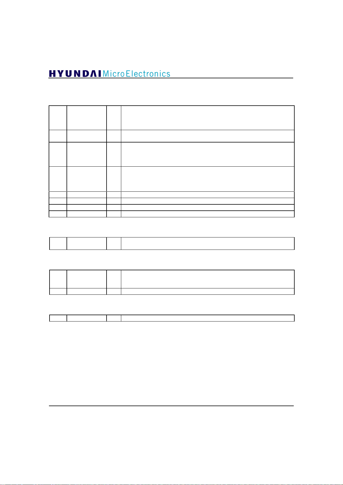
Add
ress
38
39
40
41
42
43
44
45
46
47
48
49
50
51
52
53
64
65
66
67
128
DATA BYTE
D7 D6 D5 D4 D3 D2 D1 D0
WrCoef[11:8] RdCoef[11:8] 0000XXXX
WrCoef[7::0] 00000000
RdCoef[7:0]
UpdtRngIN[9:8] MeanErrINE[18:16] MeanErrOUTE[18:16] 00XXXXXX
UpdtRngIN[7:0] 10010000
MeanErrINE[15:8]
MeanErrINE[7:0]
MeanErrOUTE[15:8]
MeanErrOUTE[7:0]
MenErrOUTP[18:16] UPlimitIN[9:8] UDlimitIN[9:8] DCinformRD[8] XXX0111X
MenErrOUTP [15:8]
MenErrOUTP [7:0]
UPlimitIN[7:0] 00000000
UDlimitIN[7:0] 00000000
DCinformRD[7:0]
U GAINcnt[2:0] “ 1101 “ XXXX1101
Pase Viterbi_on Deint_on RSdec_on Derand_on Errorflag_ins Vsbdvalid_pol Vsbclk_sup 11111111
Err_count[7:0]
U U U Data_out_en X XXX1XXXX
Err_count[15:8]
“ 0 “ X 0XXXXXXX
Initial
Value
Where U: unused register bit, X: don’t care
19
Page 19
5.3 I2C Bus Register Description
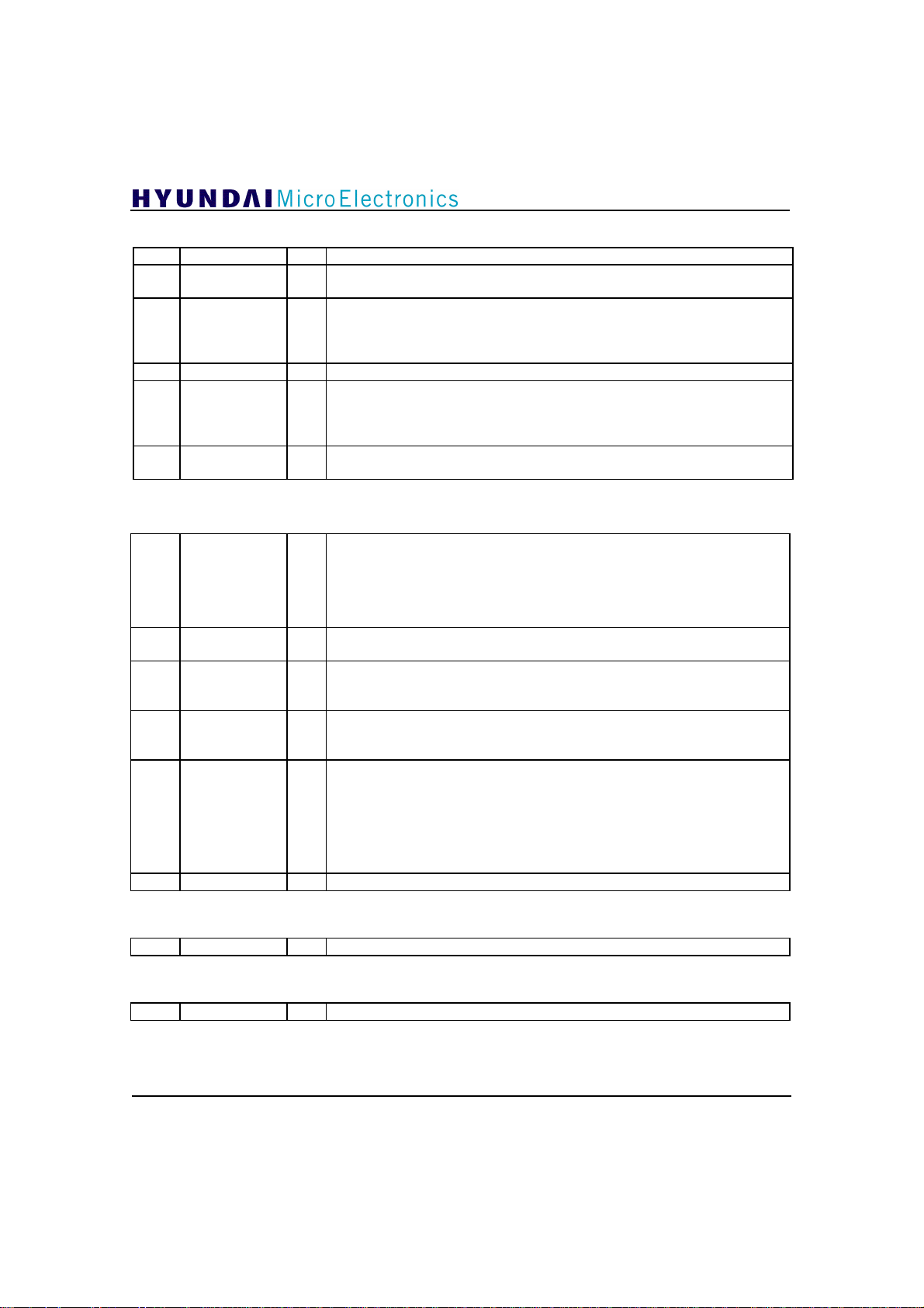
Address 0:
Most significant bit (MSB) inversion control signal of data input (DIN[9:0]).
7 Dinmode W
6 Dinsel W
5 ADCCLKSEL W
4 ADCCLKPH W
3 DCbypass W DC remove block bypass (active high). Initial value is ‘ 0’.
2 DChold W DC remove block hold (active high). Initial value is ‘0’ .
1 AGChold W AGC block hold (active high). Initial value is ‘0’.
0 AGCoffsetW W AGC offset write enable (active high). Initial value is ‘0’.
Address 1:
AGCoffset
[7:0]
[7:0]
If data input form is unsigned, the MSB of digital data input should be inverted
because all of functions in this chip use their complement data. If this bit is set
to ‘1’, it indicates the inversion of MSB. Initial value is ‘ 1’ . (refer to table 6.3.1)
Digital data input path selection signal. If this bit is set to ‘1’, it indicates output
of the internal ADC. Initial value is ‘1’. (refer to table 6.3.1)
ADC Clock Select. When the frequency of VCXO is 2fs(21.52MHz), the output
frequency of ADCCLK can be one of the two following frequencies,
fs(10.76MHz) and 2fs. If this bit is set to ‘1’, the frequency of ADCCLK is
always fs. Initial value is ‘1’. (refer to table 6.2.1)
ADC Clock Phase Select. This signal can choose one of the ADCCLK output
phases. If this bit is set to ‘0’, the ADCCLK output phase is rotated 180° off with
respect to CLKFS phase, and otherwise 0°. Default value is ‘1’. (refer to table
6.2.1)
AGC offset value. If AGCoffsetW is set to ‘1’, this signal is used for the
W
reference of AGC block. Default value is “01100000”.
GDC21D003
Address 2:
[7:5]
VSBmod[2:0] W
[4:0] W Initial value is “10010”. It would be better set to “10110”.
VSB mode signal. If VSBmodW is set to ‘1’, this signal is used for VSB mode
signal. Otherwise the VSBmod[2:0] signal is generated internally. Initial value
is “101”.
Address 3:
[7:0] W Always set to “11001000”.
20
Page 20
Address 4:
[7:6] W Initial value is “00”. It would be better set to “01”.
5 PolarityW W
4 Polarity W
[3:2] W Always set to “10”.
1 nSyncLockrst W
0 VSBmodW W
Polarity signal write enable. If this bit is set to ‘1’, it means write enable.
Initial value is ‘0’.
Polarity signal for polarity control and DATAPOLP/DATAPOLN. If
PolarityW is ‘1’, this signal is used for polarity control and the generation of
DATAPOLP/DATAPOLN signal output. Otherwise the polarity control block
uses internally calculated signal. Initial value is ‘0’. (refer to table 6.3.2)
nSyncLock reset control signal. If this bit is set to ‘0’, nSyncLock signal isn't
initialized by the change of VSB mode. Otherwise, nSyncLock signal is
initialized and changed to ‘0’ for the next Field sync duration. Initial value is
‘0’.
VSB mode write enable. If this bit is set to ‘1’, it means write enable.
Initial value is ‘0’.
Address 5:
VCXO Selection. These pins should be set as follows according to the output
[7:6]
5 nCombW W
4 nComb W
3 Combouthalf W
[2:1]
0 W Always set to ‘0’.
VCXOSEL
[1:0]
NoCombgain
[1:0]
frequency of VCXO.
VCXOSEL[1:0] The output frequency of VCXO
W
00 fs(10.76Mhz)
01 2fs(21.52Mhz)
Initial value is “00”.
nComb signal write enable. If this bit is set to ‘1’, it means write enable.
Initial value is ‘0’.
Comb filter ON/OFF signal. If nCombW are ‘1’, this signal is used for Comb
filter ON/OFF signal. Otherwise the Comb filter ON/OFF signal is generated
internally. Initial value is ‘1’.
Comb filter output gain selection signal. If this bit is set to ‘0’, the gain of the
Comb filter output is 1. Otherwise its gain is 1/2. When Comb filter is activated
this signal is valid. Initial value is ‘1’.
NoComb path gain selection signal. The gain is as follows;
NoCombgain[1:0] the gain of normal path
“00” 1(0dB)
W
“01” 1.125(1.023dB)
“10” 1.1875(1.493dB)
“11” 1.25(1.938dB)
Initial value is “01”.
GDC21D003
Address 6:
[7:0] DCvalue[7:0] R Calculated DC value of input data.
Address 7:
[7:0] R don’ t care
21
Page 21
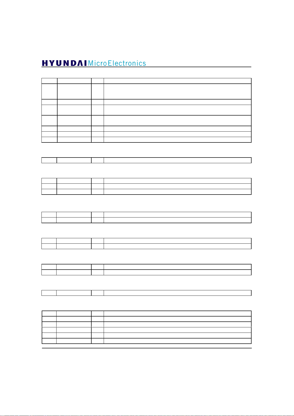
GDC21D003
Address 8:
7 R don’t care
Stability Indication of Data Sync Recovery block (active low). If the value of
6 nSyncLock R
5 nSegLock R Stability Indication of Data Segment Sync Recovery (active low).
4 Combstat R
3 nVSBmodstart R
2 DATAPOLN R Inverted polarity signal of input data.
1 nPolLock R Stability Indication of Polarity Decision (active low).
0 nFldLock R Stability Indication of Field Sync Recovery (active low).
Address 9:
[7:0] R don’ t care
Address 10:
[7:6] R don’ t care
5 nFrmLock R Stability Indication of inverted/non-inverted Field decision (active low).
4 nVSBLock R Stability Indication of current VSB mode detection (active low).
this bit is ‘0’, Data Segment Sync Recovery and Field Sync Recovery blocks
are stable.
Comb filter ON/OFF status. If the value of this bit is ‘0’, it indicates the Comb
filter is ON.
Start indication of VSB mode detector which in the Equalizer. If the value of
this bit is ‘1’, it means detector is reset.
Address 11:
[7:3] R don’ t care
[2:0]
VSBmodA[2:0]
R Internally decided VSB mode.
Address 12, 13:
[7:0] R don’ t care
[7:0] R don’ t care
Address 14:
[7:1] R don’ t care
0 nCombLock R Stability Indication of Comb filter ON/OFF decision (active low).
Address 15:
[7:0] R don’ t care
Address 32 :
7 nSyncLockPH R the state of the nSyncLock at the output of Phase Tracker
4 nCombPH R indicates whether comb filter is on or not at the output of Phase Tracker
3 nSyncLockEQ R the state of the nSyncLock at the output of Equalizer
2 nDSsyncEQ R the state of Data Segment Sync at the output of Equalizer
1 nFsyncEQ R the state of Field Sync at the output of Equalizer
0 nCombEQ R indicates whether Comb filter is on or not at the output of Equalizer
22
Page 22
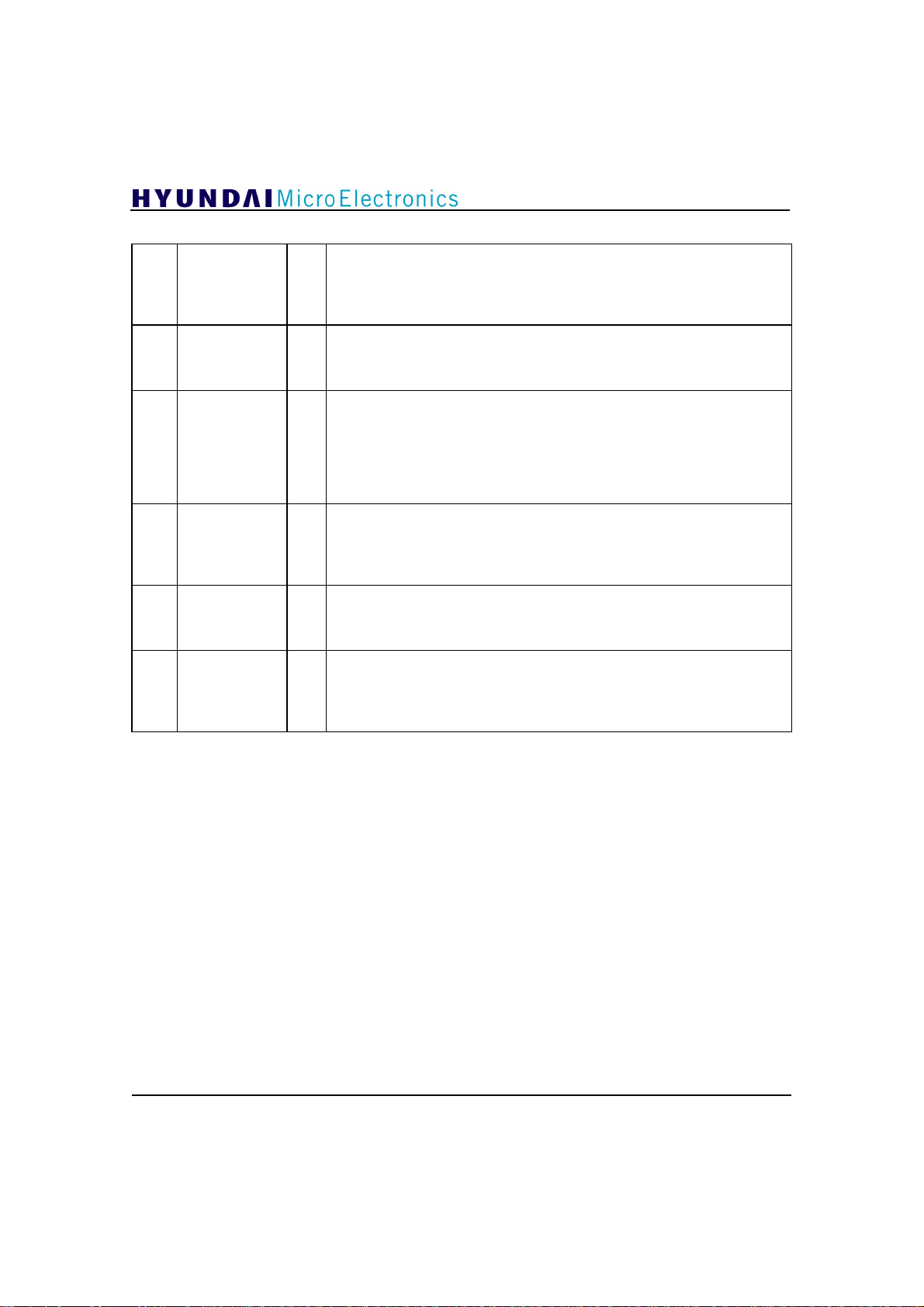
Address 33 :
7 nFreezePHI2
6 InitPHI2
PHASmodeIN
[5:4]
[1:0]
3 nFreezeEQI2
2 InitEQI2
STEPsizeIN
[1:0]
[1:0]
GDC21D003
‘0’ : Freezes the Phase Tracker in the device, which means phase tracking does
not occur.
‘1’ : normal operation
W/R
If you want to control Phase Tracker fast, use external input pins.
Initial value is ‘1’.
‘1’ : Initialize the Phase Tracker in the device.
‘0’ : normal operation
W/R
If you want to control Phase Tracker fast, use external input pins.
Initial value is ‘0’.
There are three loops in the Phase, which are gain, offset, and phase loop
Tracker.
00 : all loops on
01 : offset loop off
W/R
10 : offset and gain loops off
11 : all loops off
Initial value is “00”.
‘0’ : Freezes the Equalizer in the device, which means coefficient update does
not occur.
W/R
‘1’ : normal operation
If you want to control Equalizer fast, use external input pins.
Initial value is ‘1’.
‘1’ : Initializes the Equalizer in the device.
‘0’ : normal operation
W/R
If you want to control Equalizer fast, use external input pins.
Initial value is ‘0’.
There are three available step-sizes in the Equalizer.
10,11 : smallest step-size
W/R
01 : middle step-size
00 : largest step-size
Initial value is “11”.
23
Page 23
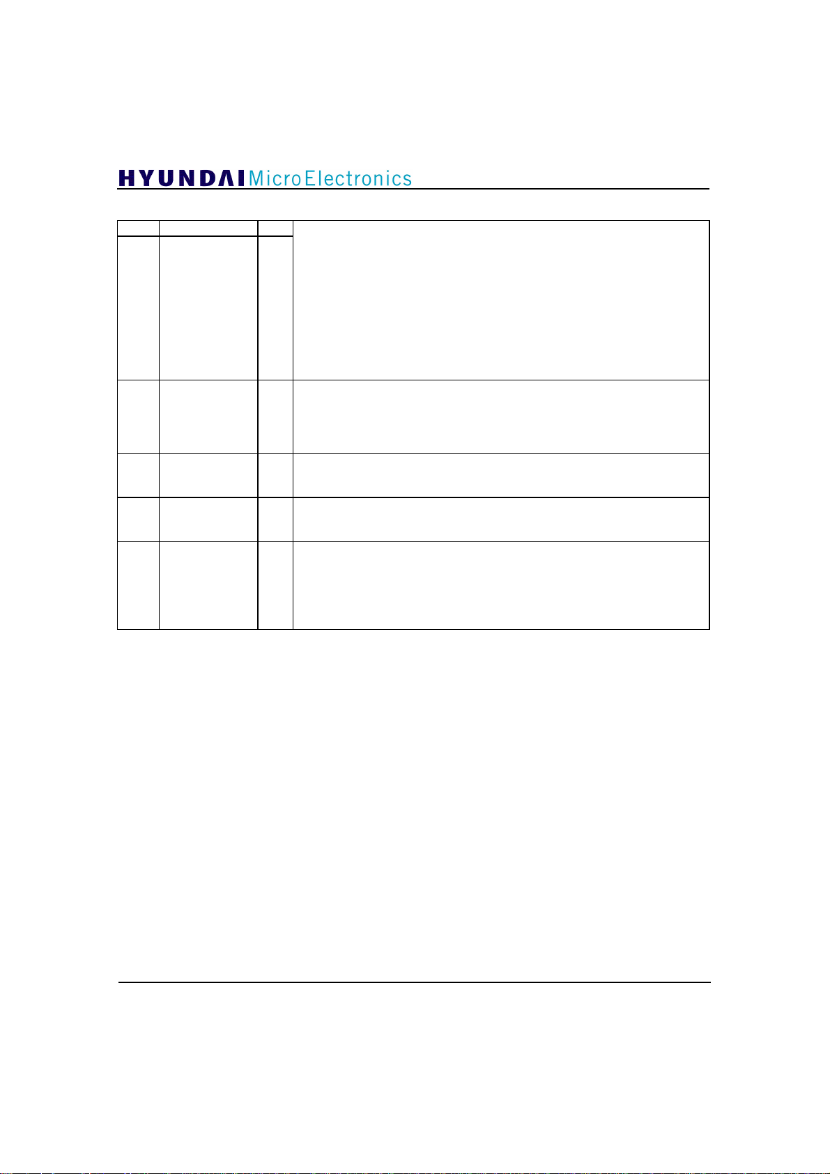
Address 34 :
7 EQmodeTIN
[6:5]
4 CombOutHalfIN
3 nDSadptIN
2 nEQoutIN
[1:0] FLTtestIN[1:0]
TRAINmodeIN
[1: 0]
GDC21D003
Updating range of the training sequence. The range value can be changed with
W/R
combination of these three bits. Initial value is “000”.
EQmodeTIN is ‘0’
00 : 574 symbols of field sync are used for equalization.
01 : 637 symbols of field sync are used for equalization.
10 : 700 symbols of field sync are used for equalization.
W/R
11 : 820 symbols of field sync are used for equalization.
EQmodeTIN is ‘1’
00 : 574 symbols of field sync are used for equalization.
01 : 637 symbols of field sync are used for equalization.
10,11 : 700 symbols of field sync are used for equalization.
Comb filter output gain selection signal.
‘0’ : the gain of the Comb filter output is 0
‘1’ : the gain of the Comb filter output is 1/2
W/R
When Comb filter is activated this signal is valid.
Initial value is ‘1’.
‘0’ : uses data segment during equalization.
‘1’ : not uses data segment during equalization.
W/R
Default value is ‘0’.
‘0’ : noise removed output from Equalizer
W/R
‘1’ : bypassed output
Initial value is ‘0’.
The location of center tap can be changed using these two bits. Initial value is
“00”.
00 : Center tap is 32nd tap
W/R
01 : Center tap is 44th tap
10 : Center tap is 52nd tap
11 : Center tap is 60th tap
24
Page 24
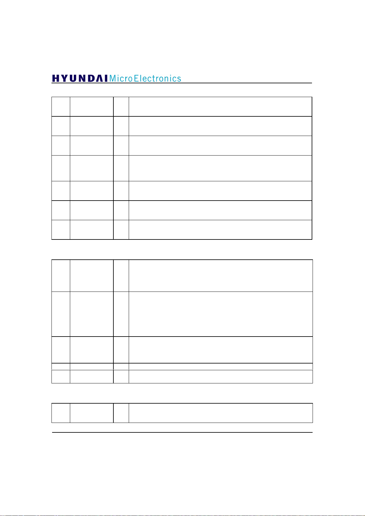
Address 35 :
7 nIIR16ONIN
6 nIIRONIN
5 nAdtOnDataI2
[4:3]
2 nRingENIN
1 nCoefRead
0 nMakeRingIN
BLNDmodeIN
[1:0]
Address 36:
[7:6] PredicIN[1: 0]
[5:3]
2 nOPERmodeIN
1 nDNgainIN
0 nDNgainThIN
LOOPgainIN
[2 : 0]
GDC21D003
‘0’ : feedback filter is on in 16 VSB mode
W/R
‘1’ : feedback filter is off
Initial value is ‘1’.
‘0’ : feedback filter is on in 2, 4 and 8 VSB mode
‘1’ : feedback filter is on only in 8 VSB mode
W/R
Initial value is ‘0’.
‘0’ : coefficient adaptation during training sequence and data interval
‘1’ : coefficient adaptation during training sequence interval only
W/R
Initial value is ‘1’. If you want to control Equalizer fast, use external input pins.
“00” : does not use blind equalization
“01” : uses blind equalization with 4-level data
W/R
“10”, “11” : uses blind equalization with 2-level data
Initial value is “00”.
‘1’ : can not change nMakeRingIN
‘0’ : can change nMakeRingIN
W/R
Initial value is ‘1’.
‘0’ : read coefficient
W/R
‘1’ : write coefficient
Initial value is ‘1’.
‘0’ : can read and write the coefficients
‘1’ : normal operation
W/R
Initial value is ‘1’.
Determines whether to use slice predictor in Phase Tracker. Initial value is “11”.
“00” : Slice Prediction is OFF.
W/R
“01” : not use.
“10” : not use.
“11” : Slice Prediction is ON.
Determines use of automatic gain routine and type of loop gain to be used in
Phase Tracker. Initial value is “000”.
“000” : Automatic gain change.
“001” : phase tracker is OFF.
W/R
“010” : smaller gain.
“011” : normal gain.
“1xx” : not use.
Sets the operation mode
‘0’ : -60° ~ 60°
W/R
‘1’ : -45° ~ 45°
Initial value is ‘0’.
Choose the value of loop gain. Initial value is ‘1’.
W/R
Choose the threshold value of loop gain when gain loop is used in automatic
W/R
mode. Initial value is ‘1’.
Address 37:
TapAddress
[7:0]
[7: 0]
Filter tap address in Equalizer. Initial value is “00000000”.
address 0 to address 63 : feed forward filter
W/R
address 64 to address 255 : feed back filter
25
Page 25
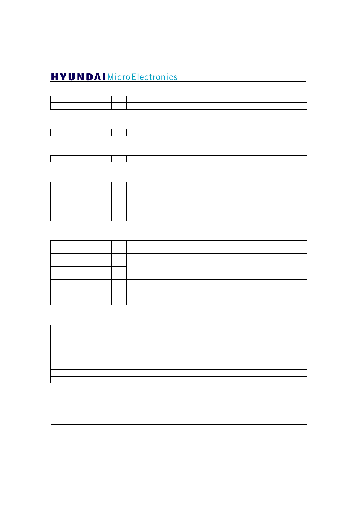
Address 38:
[7:4] WrCoef[11: 8]
[3:0] RdCoef[11: 8] R Coefficients to be read from the Equalizer filter.
Coefficients to write to the Equalizer. Default value is “0000”.
W/R
Address 39:
[7:0] WrCoef[7: 0]
Coefficients to write to the Equalizer filter. Initial value is “00000000”.
W/R
Address 40:
[7:0] RdCoef[7: 0] R Coefficients to be read from the Equalizer filter.
Address 41:
[7:6]
[5:3]
[2:1]
UpdtRngIN[9: 8]
MeanErrINE
[18: 16]
MeanErrOUTE[
18: 16]
Data range to be updated when nAdtOnDataI2 is ‘0’. Initial value is “00”. This
W/R
is 10-bit number.
R Mean squared error at the input of equalizer. This is 19-bit number.
R Mean squared error at the output of equalizer. This is 19-bit number.
Address 42, 43, 44, 45, 46:
[7:0]
[7:0]
[7:0]
[7:0]
[7:0]
UpdtRngIN[7:0]
MeanErrINE
[15 : 8]
MeanErrINE
[7 : 0]
MeanErrOUTE[
15: 8]
MeanErrOUTE[
7: 0 ]
Data range to be updated when nAdtOnDataI2 is set Initial value is
W/R
“10010000”.
R
Mean squared error at the input of Equalizer
R
R
Mean squared error at the output of Equalizer
R
GDC21D003
Address 47:
[7:5]
[4:3]
[2:1] UDlimitIN[9 : 8]
0 DcinformRD[8] R Information of DC value. This shows the current DC value in DC reduction.
0 DcinformRD[8] R Information of DC value. This shows the current DC value in DC reduction.
MeanErrOUTP
[18 : 16]
UPlimitIN
[9 : 8]
R Mean squared error at the output of Phase Tracker. This is 19-bit number.
10-bit 2’s complementary number and this should be positive number. If error of
W/R
equalizer is larger than this limit, forces error to zero. Default value is “01”.
10-bit 2’s complementary number and this should be negative number. If error
of equalizer is smaller than this limit, it is forced to be zero. Default value is
W/R
“11”.
26
Page 26
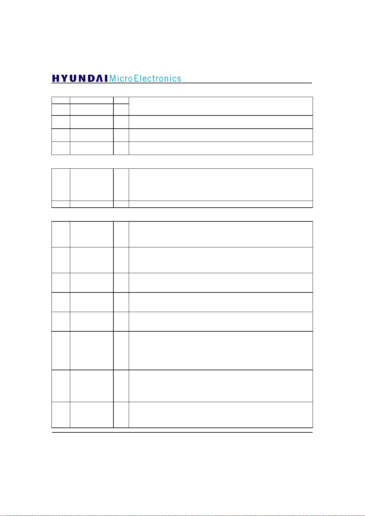
Address 48, 49, 50, 51, 52:
[7:0]
[7:0]
[7:0] UPlimitIN[7 : 0]
[7:0]
[7:0]
MeanErrOUTP[15 : 8]
MeanErrOUTP
[7:0]
UDlimitIN[7 : 0]
DcinformRD
[7:0]
R
Mean squared error at the output of Phase Tracker
R
2’s complementary number. If error of Equalizer is larger than this limit, it is
W/R
forced to be zero. Initial value is “00000000”.
2’s complementary number. If error of Equalizer is smaller than this limit, it is
W/R
forced to be zero. Initial value is “00000000”.
R Information of DC value. This shows the currently DC value in DC reduction.
Address 53:
Shows the type of loop gain used in Phase Tracker. These bits are the results of
gain loop setting in LOOPgainIN
[6:4] GAINcnt [2:0] R
[3:0] W Always set to “1101”.
“001” : phase tracker is OFF.
“010” : smaller gain is used.
“011” : normal gain is used.
Address 64:
Parallel/serial output selection
7 Pase W
6 Viterbi_on W
5 Deint_on W
4 RSdec_on W
3 Derand_on W
2 Errorflag_ins W
1 Vsbdvalid_pol W
0 Vsbclk_sup W
‘1’ : parallel ‘ 0’ : serial
If this bit is set to ‘0’, VSBDATA[0] pin is used as serial data output and
VSBDATA[7] is used as start bit indicator of a byte. Initial value is ‘1’.
Viterbi Decoder on/off selection
‘1’ : on ‘ 0’ : off
If this bit is set to ‘0’, hard decision decoding is performed instead of viterbi
decoding. Initial value is ‘1’.
Deinterleaver on/off selection
‘1’ : on ‘ 0’ : off
If this bit is set to ‘0’, deinterleaver is bypassed. Initial value is ‘ 1’ .
RS Decoder on/off selection
‘1’ : on ‘ 0’ : off
If this bit is set to ‘0’, RS decoder is bypassed. Initial value is ‘ 1’ .
Derandomizer on/off selection
‘1’ : on ‘ 0’ : off
If this bit is set to ‘0’, derandomizer is bypassed. Initial value is ‘ 1’ .
Error flag bit insertion on/off selection. Valid only when Derand_on is set to ‘1’.
‘1’ : MSB of first data byte is set to ‘ 1’ when the packet has an uncorrected
errors(when NVSBERRFLG is ‘0’)
‘0’ : nothing is done at the MSB of first data byte although the packet has an
uncorrected errors(when NVSBERRFLG is ‘0’)
Initial value is ‘1’.
VSBDVALID polarity indicator
‘1’ : VSBDATA[7:0] is valid at VSBDVALID = ‘ 1’ interval and invalid at
VSBDVALID = ‘0’ interval.
‘0’ : polarity is inverted
Initial value is ‘1’.
VSBCLK suppression indicator
‘1’ : VSBCLK is not suppressed at VSBDVALID = “invalid” interval
‘0’ : VSBCLK is suppressed(set to 0) at VSBDVALID = ”invalid” interval
Initial value is ‘1’.
GDC21D003
27
Page 27
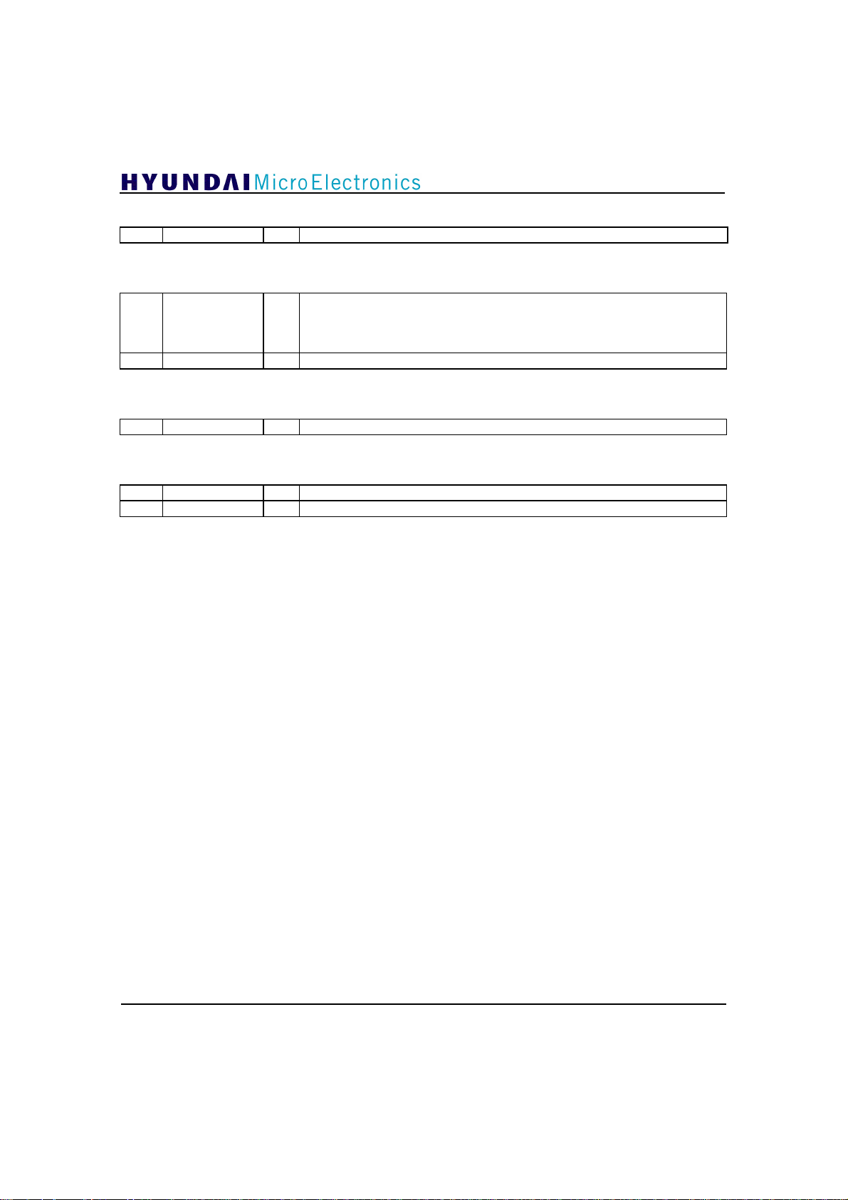
Address 65:
[7:0]
Err_count[7 : 0]
R Lower 8 bits of Segment error counter output
Address 66:
Tri-state data out
4 Data_out_en W
[3:0] R don’ t care
‘1’ : normal operation
‘0’ : high impedance
Initial is ‘1’.
Address 67:
[7:0]
Err_count[15 : 8]
R Upper 8 bits of segment error counter output
Address 128
7 W Always set to ‘0’.
[6:0] R don’ t care
GDC21D003
28
Page 28
GDC21D003
6. Functional Description
6.1 ADC
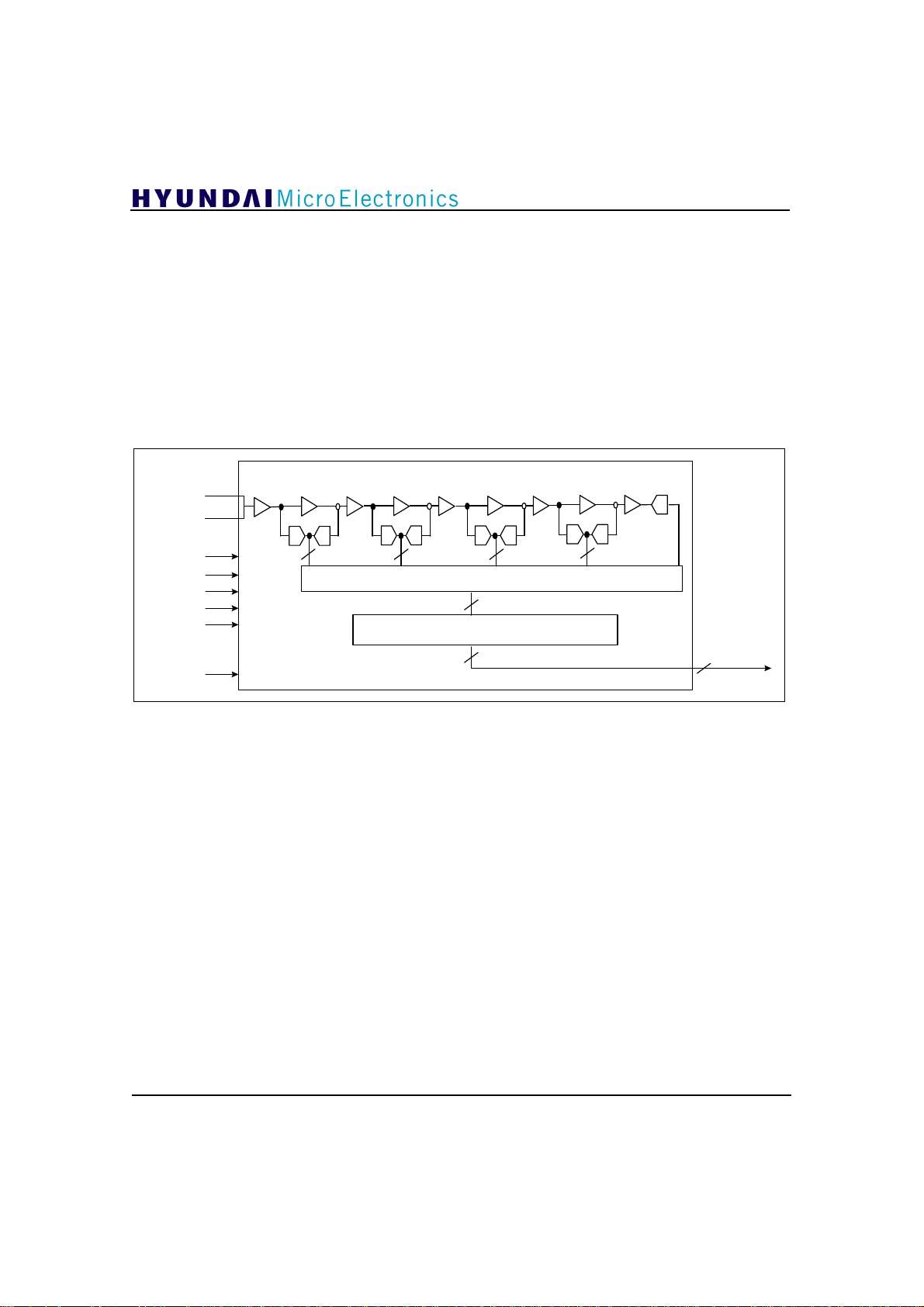
The ADC is a 10-bit 10.76Msps analog-to-digital
converter. The ADC takes samples of the
differential analog input signals at rising clock
edge and converts them into digital values. The
ADC consists of four main function blocks; SHA
block, A/D & D/A block, Correction Logic block,
and Output Buffer block. The detailed description
is as follows.
INP
INN
REFP
REFN
COM
BIAS
REF
SYMCLK
SHA SHA SHA SHA SHAGain Gain Gain Gain
A/D D/A
A/D D/A
The SHA(sample & hold amplifier) block samples
the differential analog inputs at rising clock edge.
And the following A/D & D/A(sub-A/D converter
& multiplying D/A converter) block compares the
input signal with the reference voltage and
multiplies the residue signal as the determined
gain. These processes are repeated in the
following stage. The digital outputs are generated
at each stage, corrected in the Correction Logic
block, and come out through the Output Buffer
block. Figure 6.1.1 shows the block diagram of
ADC.
A/D D/A
Correction Logic
Output Buffer
A/D
D/A
A/D
10
data output
(to synchronizer block)
Figure 6.1.1 Block Diagram of ADC
29
Page 29
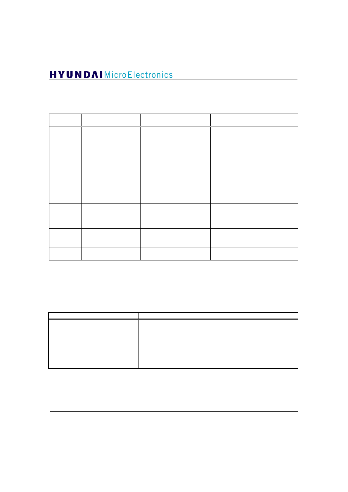
6.1.1 Electrical Characteristics
DC & AC Characteristics
(Temp = 25°C, DVDD = 3.3V, AVDD = 3.3V, COM = 1.5V)
Symbol Parameters Conditions Min. Typ. Max. Measure
INN,INP
Analog Input Voltage Differential
1.7± 0.5
I
dd
Normal Operation Fs = 10.76 Msps
Input = 1.7± 0.5V
INL
Integral
Non-Linearity
Fs = 10.76 Msps
Input = 1.7± 0.5V
(Fin*=12.2KHz sine)
DNL
Differential
Non-Linearity
Fs = 10.76 Msps
Input = 1.7± 0.5V
(Fin =12.2KHz sine)
SNR
Signal-to-Noise Ratio Fs = 10.76 Msps
Fin = 100KHz
Fs
Sampling Clock
Frequency
Ci**
Input Pin Capacitance INP = 1.7V
INN = 1.7V
Reference Resistance 12
Reference
***
V
R
REFP
ref
Top Voltage
V
REFN
Reference Bottom
***
Voltage
(NOTE) * Fin is input frequency.
** Ci = 1pF(pin capacitance) + 5pF(I/O pad capacitance)
+ 4.5pF(capacitance at the input sampling)
*** V
REFP
, V
values should be used as a pair.
REFN
1 2 Vpp
25 mA
± 4 ±6
± 1 ± 2
44 48 dB
10.76 MHz
10 pF
2.15 2.2 2.4 V
1.15 1.2 1.4 V
GDC21D003
Unit
Value
LSB
LSB
kΩ
Analog Input Voltage Level vs. Digital Output Code
Input Voltage Level Step
V
REFP
.
.
.
.
.
.
V
REFN
1023
.
.
512
511
.
.
0
MSB Digital Output Code LSB
1 1 1 1 1 1 1 1 1 1
1 0 0 0 0 0 0 0 0 0
0 1 1 1 1 1 1 1 1 1
0 0 0 0 0 0 0 0 0 0
30
.
.
.
.
Page 30
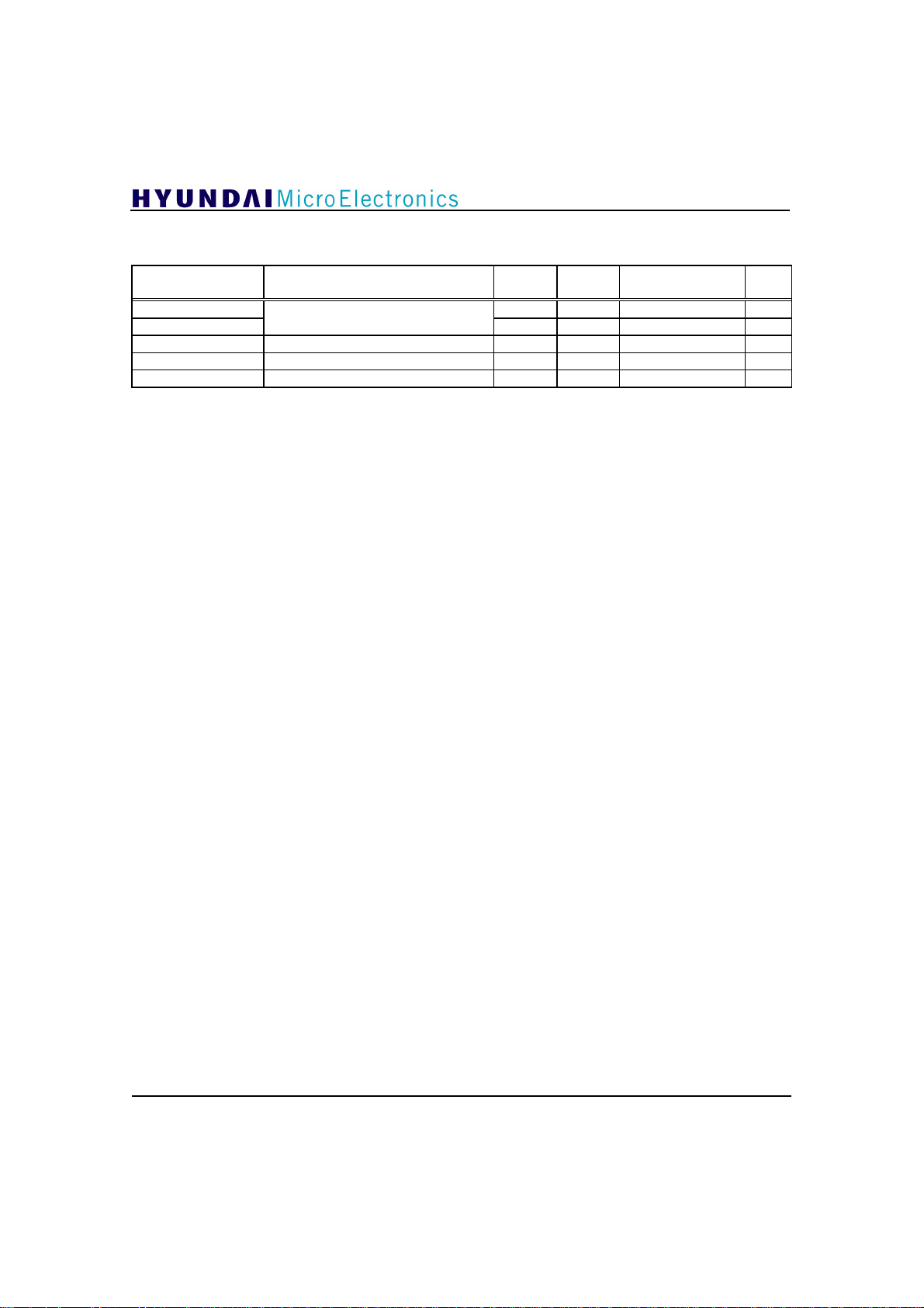
Recommended Operating Range
GDC21D003
SYMBOL PARAMETERS MIN MAX
AVDD
DGND-AGND*
REFP
REFN
R
DT
(NOTE) * The difference between analog ground and digital ground should be less than 100 mV
Power Supply
Reference Top Voltage 2.15 2.4 V
Reference Bottom Voltage 1.15 1.4 V
Clock Duty Ratio 40 60 %
3.15 3.45 V
0 100 mV
MEASURED
VALUE
UNIT
31
Page 31
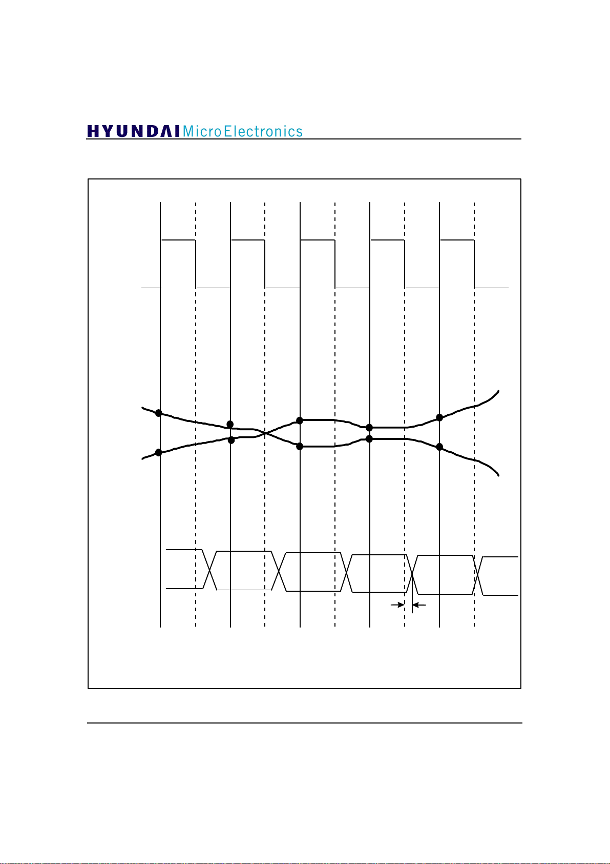
6.1.2 Timing Diagram
SYMCLK
GDC21D003
Analog
Input
Data
Output
N
N + 2
N + 1
N-3
TDL : Output Delay
: Analog Input Sampling Point
¡Ü
N-2
Figure 6.1.2 Timing Diagram of ADC
N + 3 N + 4
N-1
TDL =3ns
N
N+1
32
Page 32
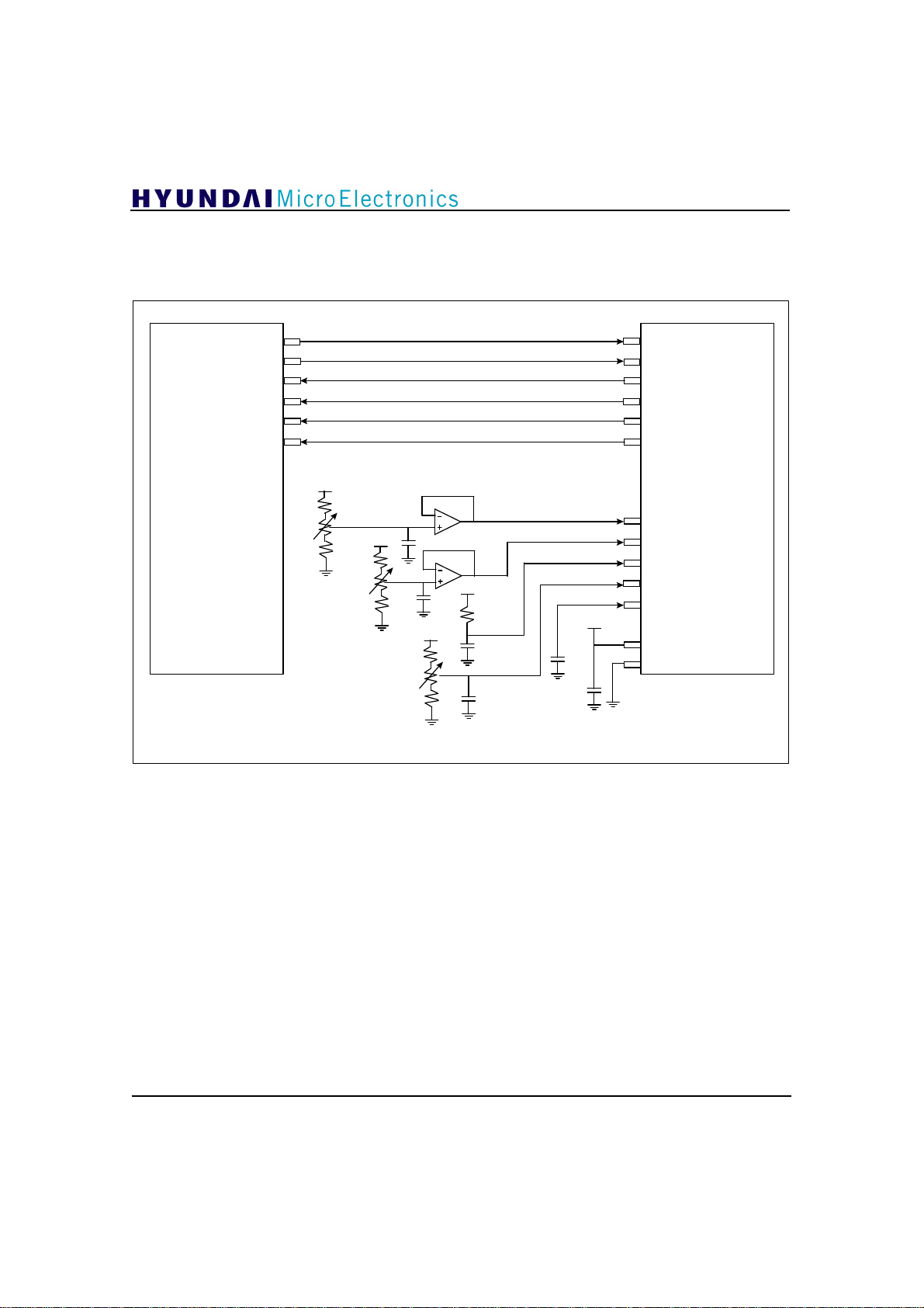
6.1.3 Application Circuits
Application Circuits
GDC21D003
SANYO
LA7785M
IOUT+
IOUT -
GUP
GDN
POLN
POLP
30
29
21
20
22
23
3.3V
1.5K
1K
3.3K
3.3K
1K
2.0K
3.3V
0.1uF
0.1uF
3.3V
3.3K
1K
2.7K
2.2V
1.2V
3.3V
12K
0.1uF
0.1uF
1.5V
Differential
_
+
(1.7 0.5V)
3.3V
0.1uF
0.1uF
125
INP
126
INN
52
GUP
53
GDN
43
DATAPOLN
44
DATAPOLP
GDC21D003
124
REFP
123
REFN
2
REF
121
COM_0
128
BIAS
AVDD
AVSS
AVDD = 3.3V, AVSS = 0V
DVDD = 3.3V, DVSS = 0V
Figure 6.1.3 ADC Application Circuit
33
Page 33
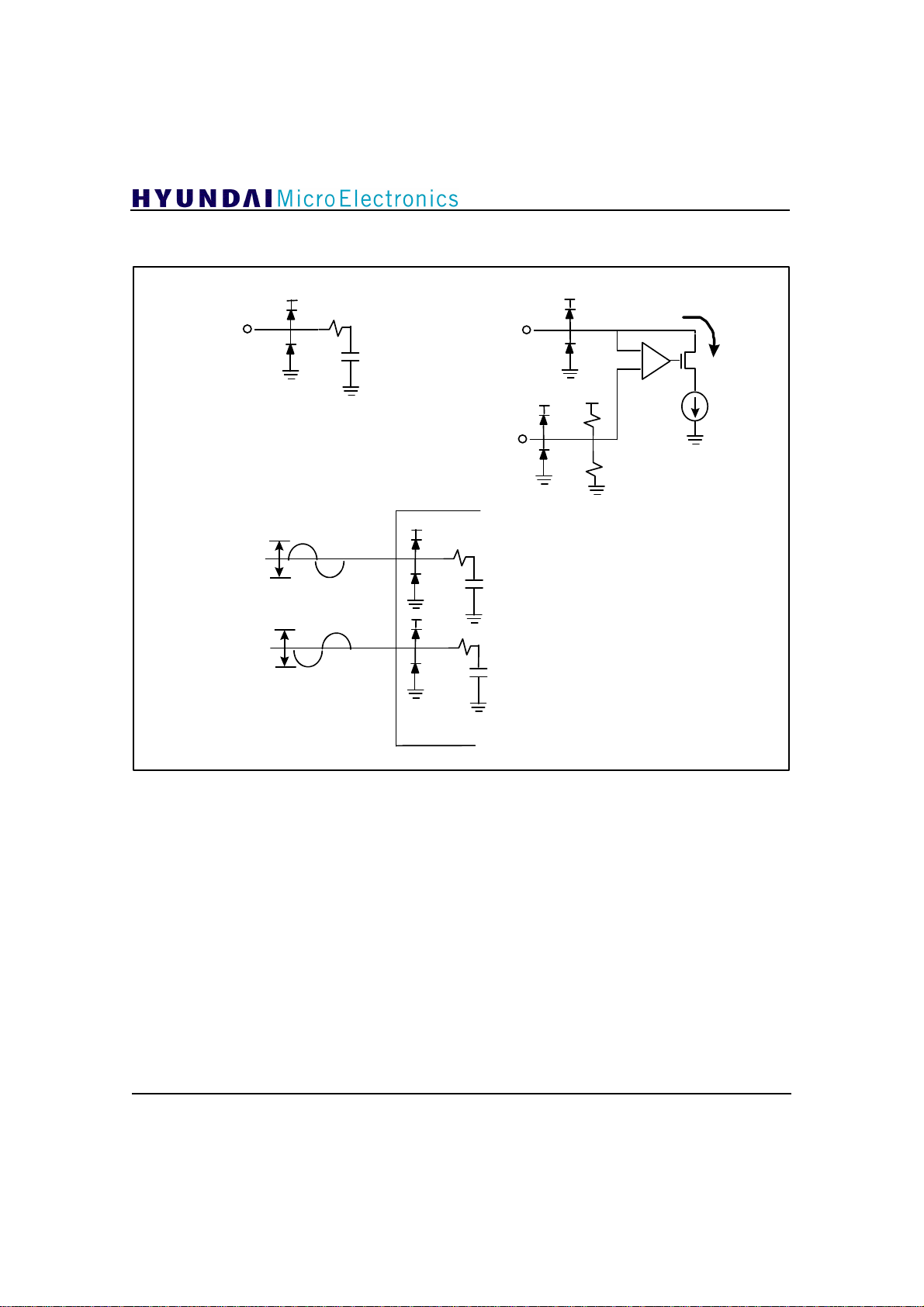
Equivalent Circuits for Bias and Input Pins
GDC21D003
REFP,REFN
COM
Differential
(1.7¡¾0.5V)
1.7V
1.7V
2.2V
1.2V
2.2V
1.2V
VDD
330~700 ohm
22pF
INP
INN
VDD
VDD
REF
BIAS
450~700 ohm
22pF
22pF
VDD
VDD
AVDD
3.6K
6.3K
10bit A/D Converter
100uA
34
Figure 6.1.4 Equivalent Circuits
Page 34
GDC21D003
6.2 Clock Divider
VSB receiver(GDC21D003) can use external
VCXO which outputs symbol frequency and its
multiple frequency because it has internal clock
divider. Multiples can be 2 times. Also, this block
has 2 output signals, CLKFS and ADCCLK.
CLKFS is used as symbol clock for DTV
transmitter, ADCCLK is used as A/D converter’s
clock when external A/D converter is used for
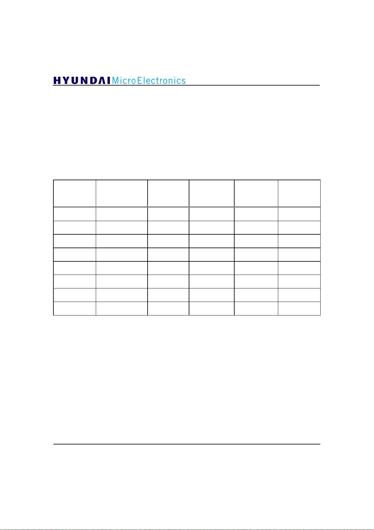
Table 6.2.1 Register Setting for Clock Divider
Frequency of
external
VCXO
10.76MHz “00” ‘0’ ‘0’ 10.76MHz
10.76MHz “00” ‘0’ ‘1’ 10.76MHz
10.76MHz “00” ‘1’ ‘0’ 10.76MHz
10.76MHz “00” ‘1’ ‘1’ 10.76MHz
21.52MHz “01” ‘0’ ‘0’ 21.52MHz
21.52MHz “01” ‘0’ ‘1’ 10.76MHz
21.52MHz “01” ‘1’ ‘0’ 21.52MHz
21.52MHz “01” ‘1’ ‘1’ 10.76MHz
VCXOSEL[1:0]
(in I2C bus
register5)
ADCCLKPH
(in I2C bus
register0)
digital input. The phase of ADCCLK against
CLKFS can vary through I2C bus. When external
VCXO output frequency is 2 times(21.52MHz) of
symbol frequency, the output frequency of
ADCCLK signal becomes the same as symbol
frequency(10.76MHz) or 2 times of symbol
frequency(21.52MH).
ADCCLK should be set through I2C bus according
to output frequency of external VCXO. The setting
of each case is described in following tale 6.2.1.
ADCCLKSEL
(I2C bus
register0)
ADCCLK
regarding
(phase: 180o)
(phase: 180o)
(phase: 0o)
(phase: 0o)
(phase: 180o)
(phase: 180o)
(phase: 0o)
(phase: 0o)
(phase
CLKFS)
CLKFS
10.76MHz
10.76MHz
10.76MHz
10.76MHz
10.76MHz
10.76MHz
10.76MHz
10.76MHz
35
Page 35
6.3 Synchronizer
GDC21D003
6.3.1 Input Control
VSB receiver(GDC21D003) use 10bits signal
generated in internal A/D converter or
INN
INP
A/D Converter
DIN[9:0]
Input Selection
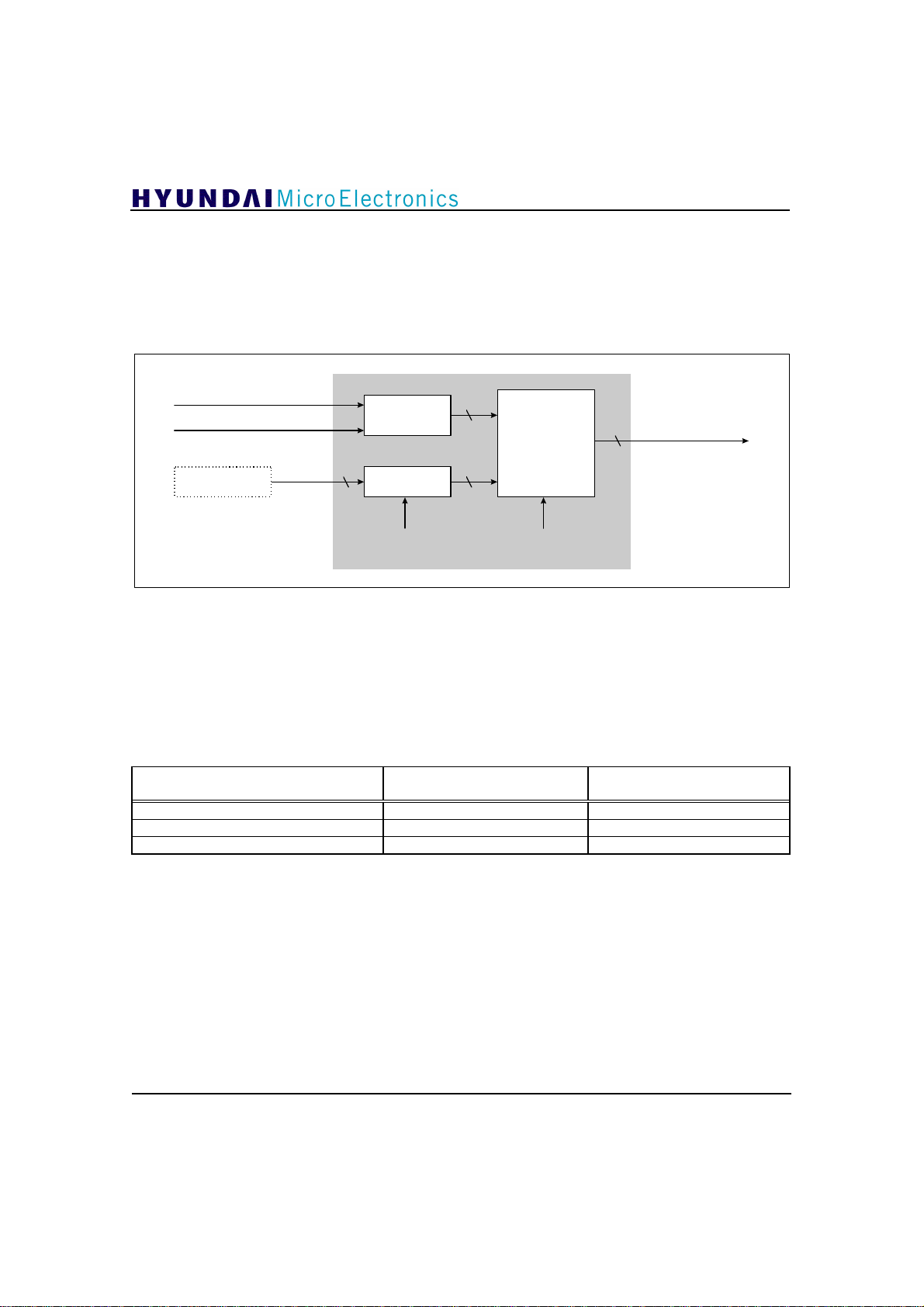
Figure 6.3.1 The Block Diagram of Input Selection
Figure 6.3.1 is internal block diagram of Input
Selection. You have to choose either the output of
internal A/D converter or that of external A/D
converter as digital input signal (Dinsel). If you
decide to use the output of external one,
A/D Converter
10
MSB Control
Internal
Dinmode Dinsel
10bits(DIN[9:0]) external data input to perform
digital processing. Therefore, the data input path
must be set according to input before digital
processing.
10
Digital Input Signal
Multiplexer
10
10
MSB(DIN[9]) of 10bits input (DIN[9:0]) should be
set according to its output characteristics(Dinmode).
Setting of Dinsel and Dinmode is performed
through I2C bus and it is as following Table 6.3.1.
Table 6.3.1 Input Signal Path Setting
Input signal path Dinmode
(in I2C bus register0)
(in I2C bus register0)
From internal A/D converter Don’ t care ‘1’
From DIN[9:0] (Signed signal) ‘0’ ‘0’
From DIN[9:0] (Unsigned signal) ‘1’ ‘0’
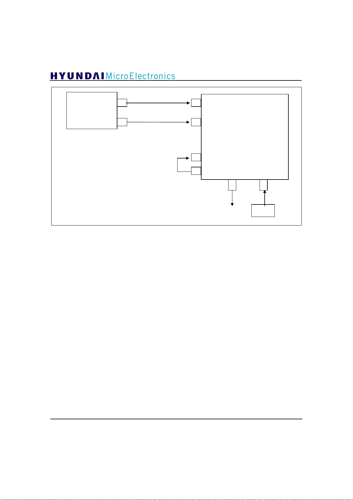
Figure 6.3.2 shows the relationship between chip
and external device in case that internal ADC
output is used for digital processing. Figure 6.3.3
device in case that ADC digital output is used for
on-chip digital processing with using other external
ADC instead of using internal ADC.
shows the relationship between chip and external
36
Dinsel
Page 36
GDC21D003
INN
ADCCLK
126
125
INP
LA7785M
(SANYO)
29
IOUT-
30
IOUT+
GDC21D003
SYMCLK
CLKFS
OPEN
VCXO
(NOTE) - Regarding external VCXO output frequency, VCXOSEL[1:0] should be set as Table 6.2.1.
- Since internal ADC is used, peripheral circuit should be set according to ADC.
- Digital input signal path should be set as Table 6.3.1 to use internal ADC.
- If VCXO output frequency is equal to symbol frequency, VCXO(pin12) can be connected to GND,
and SYMCLK(pin41) and VCXO output can be connected directly.
Figure 6.3.2 I/F Circuit Diagram between VSB Receiver & Demodulator (Internal A/D Input)
37
Page 37
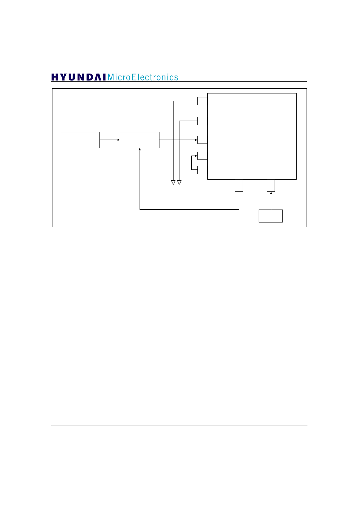
126
14
125
12
LA 7785M
GDC21D003
INN
INP
Demodulator
(SANYO)
A/D
DIN[9:0]
41
SYMCLK
18
CLKFS
GDC21D003
VCXO
(NOTE)- Regarding external VCXO output frequency, VCXOSEL[1:0] should be set as Table 6.2.1.
- Since internal ADC is used, frequency and phase of ADCCLK that is its input clock should be set as Table 6.2.1.
- Digital input signal path should be set as Table 6.3.1 to use external ADC output.
- If VCXO output frequency is equal to symbol frequency, VCXO(pin12) can be connected to GND, and
SYMCLK(pin41), A/D clock, and VCXO output can be connected directly.
Figure 6.3.3 I/F Circuit Diagram between VSB Receiver & Demodulator (External A/D Input)
38
Page 38
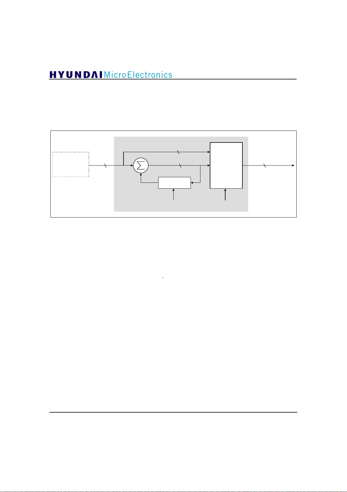
GDC21D003
6.3.2 DC Reduction
Current DTV transmission system uses pilot for
restoration of carrier signal. Inserted DC value at
transmitter is transformed into pilot in frequency
domain. In receiver, A/D is used to convert
Input Selection
10
+
-
DC Reduction
Figure 6.3.4 The Block Diagram of DC Reduction
Figure 6.3.4 is block diagram of DC Reduction.
Output of Input Selection is sent to DC Reduction
block and removes pilot as well as all DCs in
analog system. And DC value is calculated from all
data of input signal.
Through I2C bus this block can be bypassed and
DC value doesn’t be updated from current state.
Among I2C bus control signals, if DC bypass
signal(in I2C bus register0) is ‘0’, DC removed
signal is output, and if it is ‘1’, input signal is
bypassed and output. Also, when DChold
signal(in I2C bus register0) is ‘0’, DC value is
calculated using continuously input signals, when it
is ‘1’, DC value at the moment is saved without
updating DC value. Calculated DC value can be
read through I2C bus. (DCvalue[7:0] in I2C bus
register address6)
6.3.3 Auto Gain Control(AGC)
There are 2 AGC modes currently used, one is
Non-coherent AGC mode and the other is Coherent
AGC mode. Figure 6.3.5 is the block diagram of
baseband analog signal that completed the
demodulation of RF signal into digital signal, A/D
output has the same DC value inserted from
transmitter. Also DC components arise through
various analog processing.
10
10 10
Accumulator
DChold
Multiplexer
DCbypass
AGC. Non-coherent AGC mode is performed
during initialization state and before finding the
Data Segment Sync interval in receiver. During
initialization state, it increases Gain continuously
to take the maximum value.(GUP = ‘1’ during
initialization state). Also, since at the moment of
reset completion, received signal has the maximum
gain, it is highly possible that A/D converter output
has either maximum or minimum value. A/D
converter output can also have either maximum or
minimum value from too much noise within
channel. When input signal value has
maximum/minimum value for 8 symbols in a row,
control signal (GDN = ‘1’ during 2 symbols) is
generated to reduce system gain. Non-coherent
AGC mode doesn’t stop before it finds timing of
Data Segment Sync signal. Coherent AGC mode
calculates the average of input signals and controls
the GUP/GDN signal so that this average value can
have the desired value.
39
Page 39
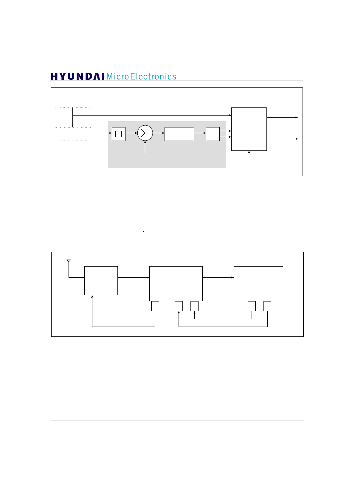
Input Selection
DC Reduction Accumulator
Coherent AGC
+
-
AGC offset
Figure 6.3.5 The Block Diagram of AGC
PWM
Non-Choerent
AGC
RESET
GDC21D003
GUP
GDN
GUP/GDN signal is transmitted to off-chip
demodulator and controls the gain of Tuner and
demodulator.
Through I2C bus, AGC block can be held(When
AGChold signal in register0 is ‘1’). And for input
data to have desired optimum value, Coherent
AGC uses reference value which can be input
through I2C bus (AGCoffset[7:0] in I2C bus
TUNER
(NOTE) RFAGC signal, an input signal to Tuner should be connected referring to LA7785M.
LA7785M
(SANYO)
RFAGC10GDN20GUP
register1) or can use already defined value. If you
want to change Coherent AGC reference value
through I2C bus, AGCoffset[7:0](in I2C bus
register1) value should be set and AGCoffsetW(in
register0) signal should be set to ‘1’. If
AGCoffsetW signal is ‘0’, already defined value is
used as a reference value. Figure 6.6 shows the
connection of chip output, GUP/GDN signal.
21
Figure 6.3.6 AGC Signal I/F for DTV System
6.3.4 Polarity Correction
phase) or 180ophase(out of phase). When carrier is
locked in 0o phase, there is no problem, but when
For currently used demodulator algorithm,
FPLL(Frequency & Phase Locked Loop) is used.
Due to FPLL algorithm’s property, demodulator
carrier is locked in 180o phase, polarity of baseband
data are all inverted. In this case, input data
polarity should be reverted.
(carrier recovery) lock can occur in 0o phase(in
GDC21D003
(LG)
GUP52GDN
53
40
Page 40
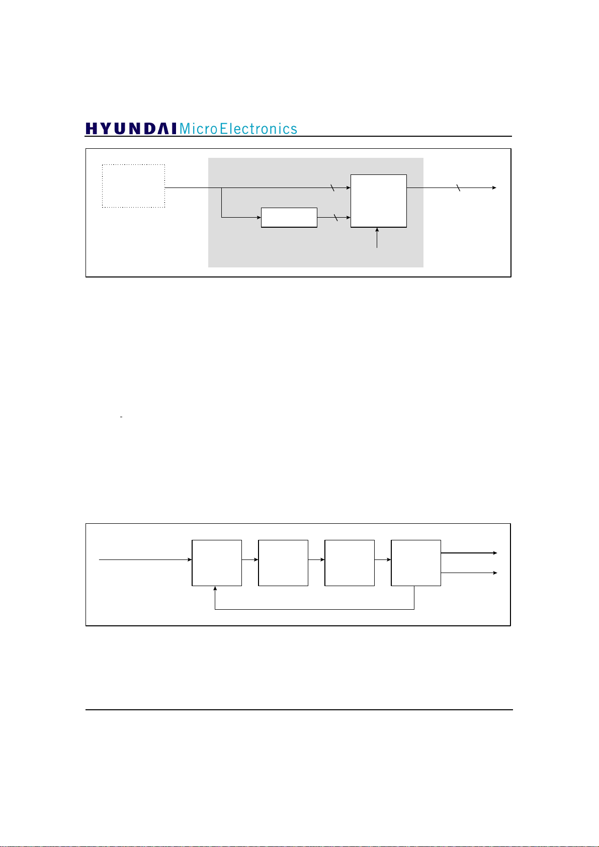
GDC21D003
DC Reduction
Polarity Correction
Fig 6.3.7 The Block Diagram of Polarity Correction
Figure 6.3.7 is Polarity Correction block diagram.
Output signal polarity is corrected by control of
polarity from Polarity Decision block.
6.3.5 Data Segment Sync Recovery
At DTV transmitter part Data Segment Sync is
inserted for 4-symbol period in every Data
Segment. This Data Segment Sync has (1,0,0,1)
pattern.
DTV receiver compares inputted signal pattern
with Data Segment Sync pattern (1, 0, 0, 1)
inputted from transmitter and acknowledges the
most similar pattern as Data Segment Sync interval.
But because the inputted signal at the beginning of
activation has polarity ambiguity generated by
FPLL, inverted polarity pattern of Data Segment
Sync (1, 0, 0, 1) from transmitter is acknowledged
as Data Segment Sync interval. After completion of
Polarity Inverse
10 10
Multiplexer
10
polarity
initial Data Segment Sync detection, input signal
polarity is detected from Polarity Decision block at
the end. Also after polarity correction in Polarity
Correction block, only positive polarity is
acknowledged as Data Segment Sync interval. And
Data Segment Sync detection becomes easier under
close Ghost environment by improving its
performance. Figure 6.3.8 shows the improved
Data Segment Sync Recovery block diagram. At
first input signal is integrated by the segment
passing through Segment Correlator. Slicer extracts
the information of Data Segment Sync interval
from output of integration period. This information
undergoes its reliability check in Confidence
Counter and then creates Data Segment Sync.
When reliability builds up to some level, nSegLock
signal is generated to inform the completion of
Data Segment Sync Recovery. This signal can read
through I2C bus(nSegLock in I2C bus register8).
output of Polarity correct
Segment
Correlator
Segment
Integrator
Figure 6.3.8 The Block Diagram of Data Segment Sync Recovery
If Data Segment Sync is found in this block, input
polarity is detected in the Polarity Decision block
and Timing Recovery block sets SEGSYNCLOCK
nSegLock
Segment
Slicer
control signal
Confidence
Counter
nSegSync
signal to ‘1’ which informs the start of activation
(Timing recovery start status). This signal is ‘0’
until it finds Data Segment Sync.
41
Page 41
GDC21D003
6.3.6 Polarity Decision
It decides input signal polarity after it finds Data
Segment Sync timing input from transmitter and
checks Data Segment Sync pattern. Data Segment
Sync pattern input from transmitter is (1,0,0,1).
Therefore when Data Segment Sync pattern of
transmitted signal is (1,0,0,1), baseband signal has
positive polarity, and when (0,1,1,0), it has
negative polarity. In this block, input Data Segment
Sync pattern is checked and output signal is
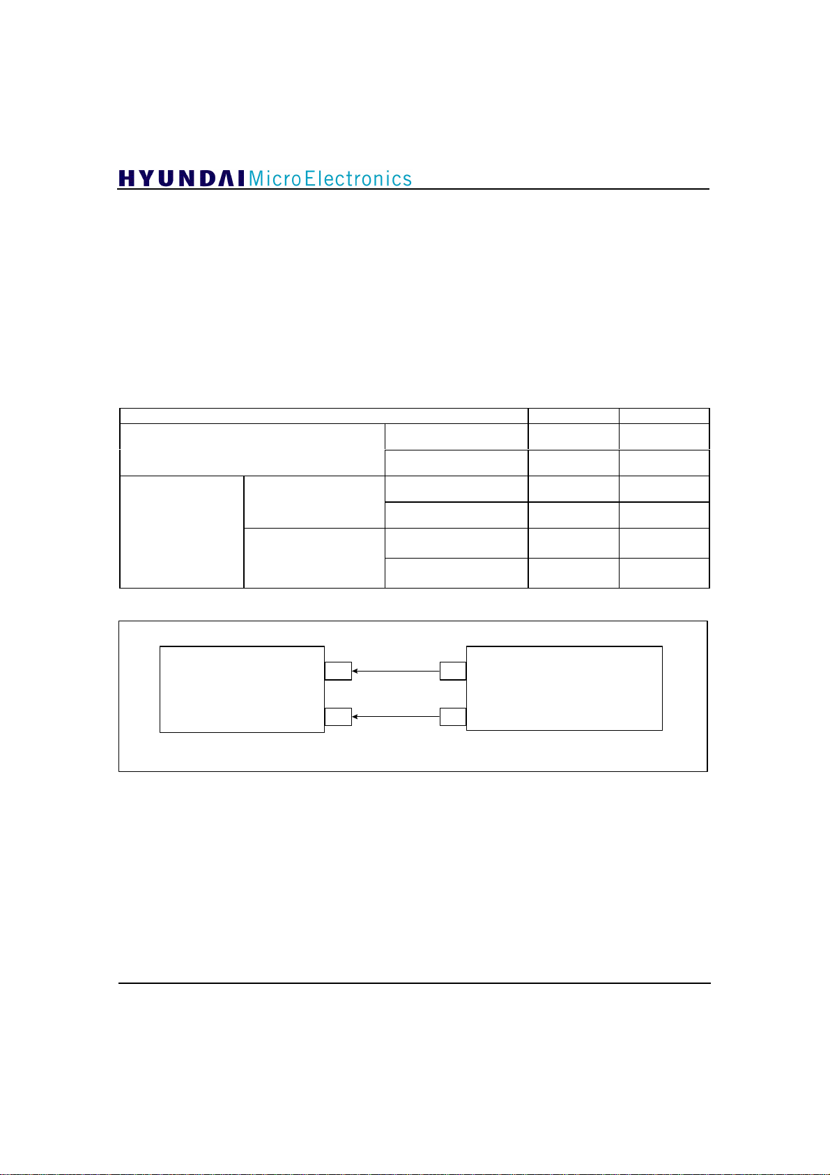
Table 6.3.2 DATAPOLP & DATAPOLN Output
(I2C bus register4)
After Data Segment
Sync Lock
PolarityW : ‘1’
(I2C bus register4)
generated by this result. Then it is sent to internal
Polarity Correction and demodulator. Also,
regardless of inputted Data Segment Sync pattern,
through I2C bus, DATAPOLP and DATAPOLN are
decided. The output of Polarity Decision, DAPOLP
and DATAPOLN are shown in Table 6.3.2. On the
other hand, DATAPOLN signal can be read
through I2C bus.(DATAPOLN in I2C bus register8)
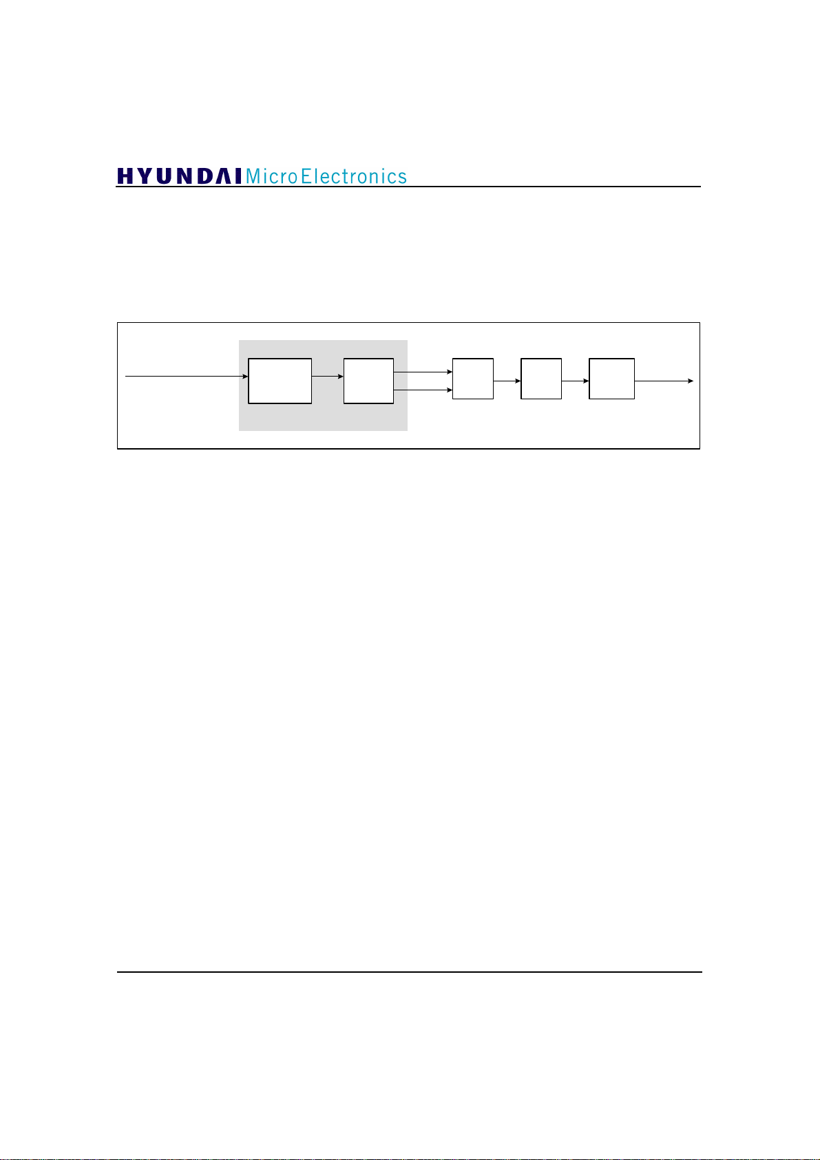
Figure 6.3.9 describes the connection of
DATAPOLP & DATAPOLN which is output of
chip and Demodulator chip.
DATAPOLP DATAPOLN
Positive polarity ‘ 0’ ‘0’Before Data Segment Sync Lock
Negative polarity ‘0’ ‘0’
Positive polarity ‘ 1’ ‘ 0’PolarityW : ‘0’
Negative polarity ‘0’ ‘1’
Polarity : ‘0’
‘1’ ‘0’
(I2C bus register4)
Polarity : ‘1’
‘0’ ‘1’
(I2C bus register4)
42
LA7785M
(SANYO)
23
POLP
22
POLN
44
DATAPOLP
43
DATAPOLN
Figure 6.3.9 Polarity Signal I/F Circuit
GDC21D003
(LG)
Page 42
GDC21D003
6.3.7 Timing Recovery
In current DTV system, timing information is
extracted from inputted Data Segment Sync signal
and the clock used for digital processing and A/D.
Timing Recovery structure used in this chip is
similar to typical PLL structure. PLL generally
output of polarity correct
Correlator PWM
Digital Phase Detector
Figure 6.3.10 Timing Recovery Block
On-chip Phase Detector extracts phase information
only in Data Segment Sync interval, and it is
activated after finding Data Segment Sync interval
inserted in transmitter. SEGSYNCLOCK(PIN46)
shows whether Data Segment Sync is found or not.
If this signal is ‘0’, Data Segment Sync isn’ t found,
if this is ‘1’, it is found.
Phase detector uses filter whose coefficient is (-1,1,1,1) because it uses Data Segment Sync
pattern(1,0,0,1) to get phase information. Phase
consists of phase detector, loop filter, and
VCO(VCXO). In this chip, Timing Recovery is
consisted of internal Digital Phase Detector,
external analog device, Charge Pump, Loop Filter
and VCXO. Figure 6.3.10 is Timing Recovery
block diagram.
CHGUP
CHGDN
Charge
Pump
Loop
Filter
VCXO
information is converted again to PWM signal and
output from chip(NCHGUP/ NCHGDN).
While SEGSYNCLOCK signal is ‘0’,
NCHGUP/NCHGDN signal outputs are all ‘0’. In
this time, external Charge Pump is charged to freerun voltage of VCXO.
When SEGSYNCLOCK signal is changed to ‘1’,
NCHGUP/NCHGDN signals are all changed to ‘1’,
and once per every Data Segment, charge of
external Charge Pump is charged up and down.
CLOCK
43
Page 43
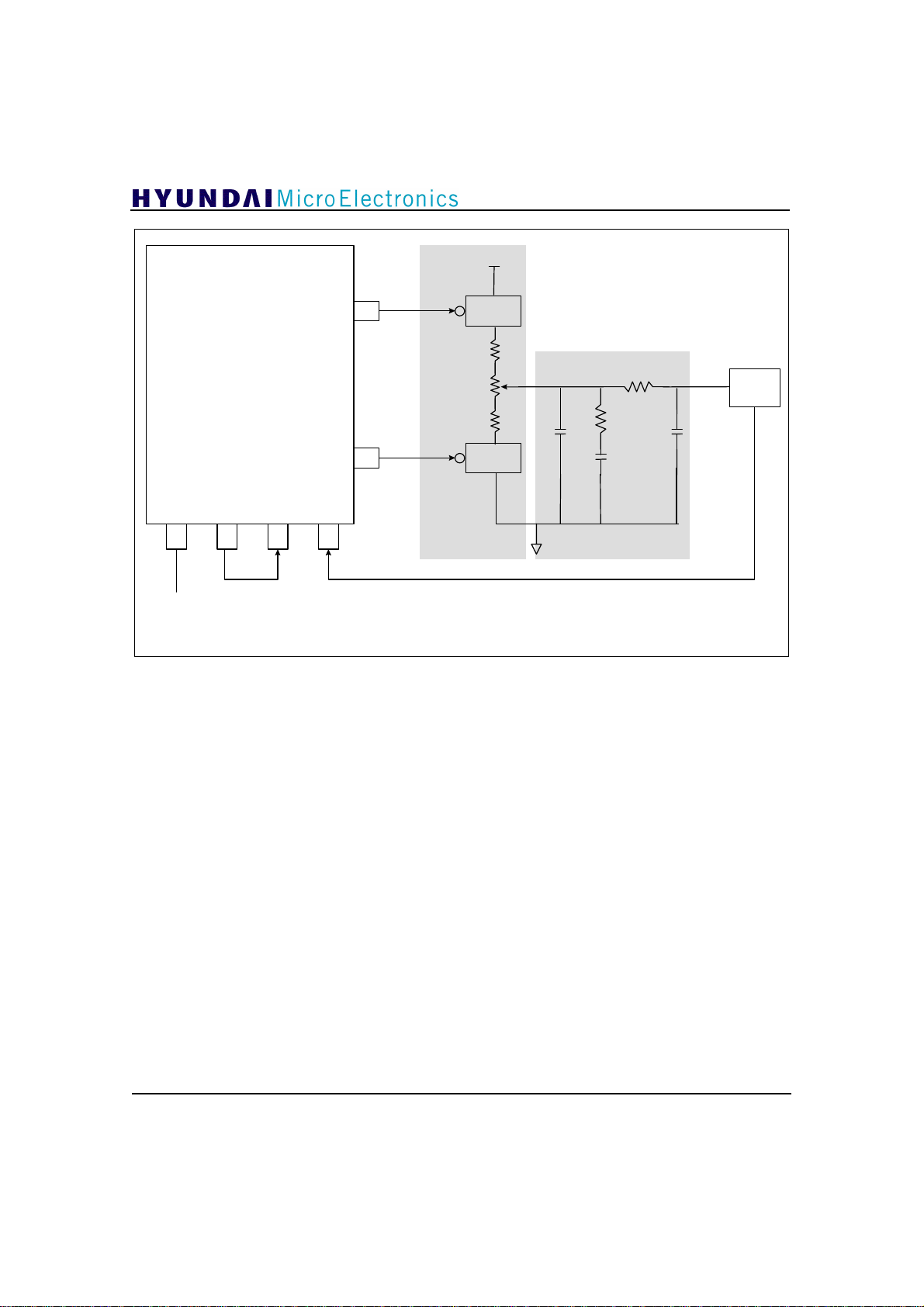
6.8K
+3.3V
0.01uF
NCHGUP
141841
VCXO
12
GDC21D003
56
GDC21D003
Analog
S/W
10K
VCXO
(LG)
57
NCHGDN
Charge Pump Loop Filter
OPEN
Or
(NOTE)- Regarding external VCXO output frequency, VCXOSEL[1:0] should be set as Table 6.2.1.
Analog
S/W
10.76MHz, 21.52MHz
- In case of using digital input by external ADC, ADCCLK frequency and CLKFS phase should be set as Table 6.2.1.
- Each discrete device value in figure is just recommended value.
- PNP type transistor can be used instead of Analog S/W.
Figure 6.3.11 Timing Recovery I/F Circuit(1)
44
Page 44
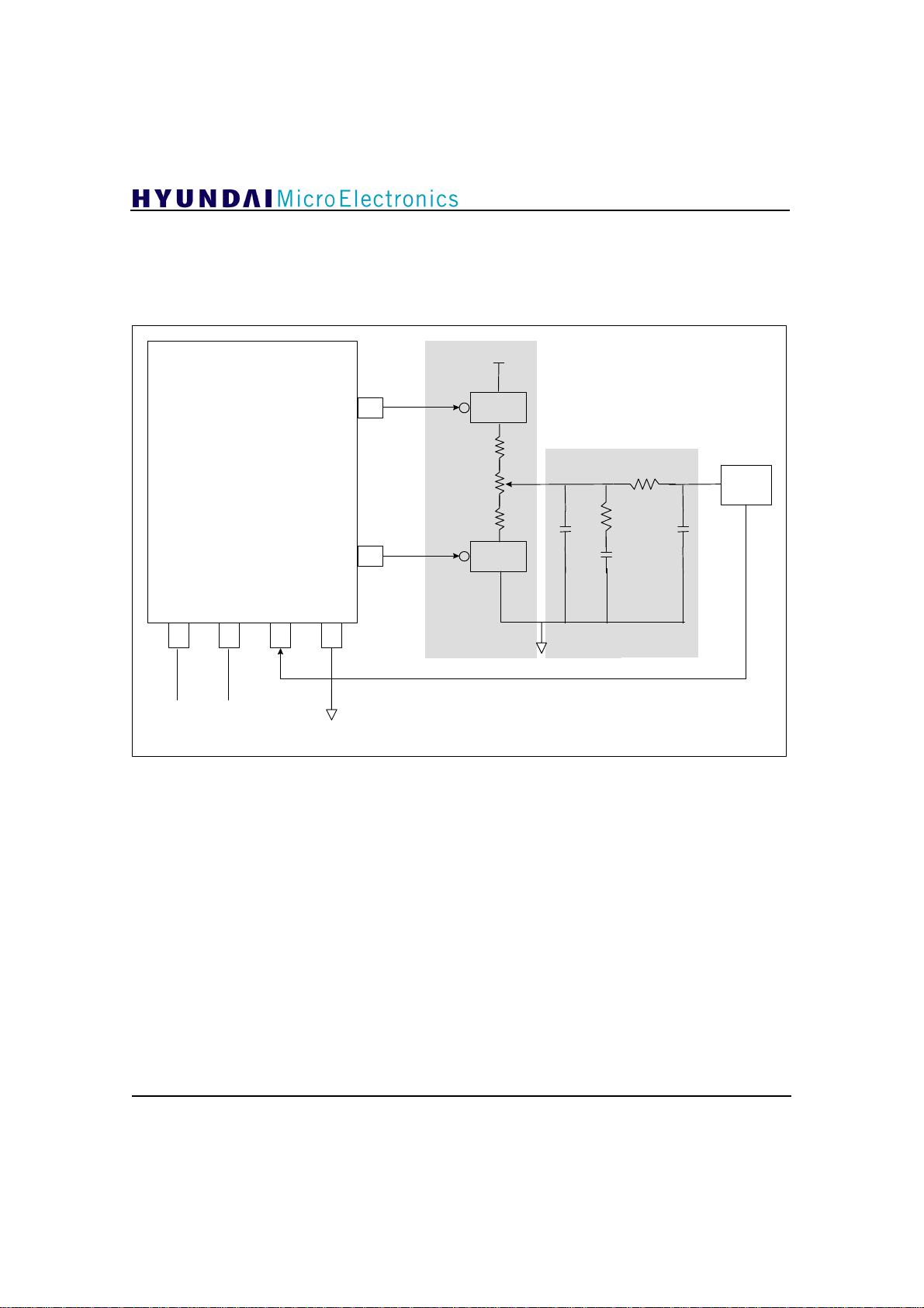
GDC21D003
6.8K
6.8K
0.01uF
ADCCLK
CLKFS
VCXO
Phase information from chip passes through
Charge Pump and is input to Loop Filter. Loop
Filter output is connected to VCXO to control
clock phase. Figure 6.3.11 shows the connection
diagram when external VCXO output frequency is
56
NCHGUP
GDC21D003
(LG)
57
NCHGDN
equal to 1 and 2 times output frequency of symbol
frequency. And Figure 6.3.12 shows the connection
diagram when external VCXO output frequency is
equal to that of symbol frequency.
+3.3V
Analog
S/W
10K
VCXO
Analog
S/W
Charge Pump Loop Filter
10.76MHz
OPEN
Or
To ADC
(NOTE) - ADCCLK frequency and CLKFS phase should be set as Table 6.2.1 when digital input using external ADC
is used.
OPEN
- Each discrete device value in this figure is just recommended value.
- Analog S/W should be ON when input signal (NCHGUP/NCHGDN) is ‘0’ .
- PNP type transistor can be used instead of Analog S/W.
Figure 6.3.12 Timing Recovery I/F Circuit(2)
45
Page 45
GDC21D003
6.3.8 Field Sync Recovery
Transmitter inserts 1 Data Segment long Field Sync
every 313th segment. Inserted Field Sync structure
is described in Figure 6.3.13. Field Sync is found
Segment
sync
(4 symbols)
Among three PN63 signals exceptionally the
second one changes its polarity in every Field.
Equalizer uses this data interval, so polarity
information(FOE : pin number 66) should be
detected. This polarity information detection starts
PN511
(511 symbols)
Error
Calculation
PN63
(63 symbols)
Figure 6.3.13 Field Sync Structure
PN63*
(63 symbols)
Minimum
Error
Detection
using PN511 as shown in Figure 6.3.13. Cause
pattern of PN511 input from transmitter is already
acknowledged, by comparing with transmitted
signal, the interval having the most similar pattern
is acknowledged as Field Sync interval.
PN63
(63 symbols)
VSB mode
(24 symbols)
reserved
(92 symbols)
12 symbol
data
(12 symbols)
after finding Field Sync. Used algorithm is similar
to that of Field Sync case. If the second PN63
phase is the same as others, FOE signal outputs ‘0’,
otherwise it outputs ‘1’.
nSyncLock
Confidence
Counter
nFsync
nFldLock
Reference
Generation
Figure 6.3.14 The Block Diagram of Field Sync Recovery
Figure 6.3.14 is the block diagram of Field Sync
Recovery. Input signal calculates error value by the
Data Segment, comparing with Reference
Generation output. Among these error values, the
smallest Data Segment is acknowledged as Field
Sync interval, Confidence Counter checks its
confidence and generates Field Sync. And after
finding Field Sync it detects Polarity Error of the
46
Polarity
Error
Detection
Foe
nFrmLock
second PN63 interval in Error Calculation output
and generates Foe signal.
Field Sync Recovery generates nVSBmodstart(in
I2C bus register8) and nSyncLock(in I2C bus
register8) signal. nVSBmodstart signal is used as
initialization signal of VSB Mode Detect block.
When this signal is ‘1’, it means the initialization
state, when it is ‘0’, it means the operation state.
Page 46
GDC21D003
This signal is changed to ‘0’ after detection of the
Field Sync signal. Then VSB Mode Detect is
activated. nSyncLock signal is used for
initialization of NTSC Rejection, Equalizer, Phase
Tracker, and Channel Decoder(FEC). If this signal
is ‘1’, it means the initialization state, if it is ‘ 0’ , it
means the operation state. This signal is changed to
‘0’ after detection of the Field Sync signal and
FOE signal. If detected VSB mode from VSB
mode detect is different from existing one, NTSC
Rejection, Equalizer, Phase Tracker, and Channel
Decoder(FEC) are operated in new VSB mode. But
since Equalizer and Phase Tracker are consisted of
lots of feed back loops, these 2 blocks operated in
existing VSB mode can be invalid when they
suddenly should be operated on new VSB mode. In
this case, nSyncLock signal can initialize again
these blocks for normal operation, which may bring
the increase of system Lock up time. These 2 cases
have trade-off respectively that nSyncLock signal
can be initialized through nSyncLockrst(in I2C bus
register4) signal or not on the change of VSB mode.
If nSyncLockrst signal is ‘0’, it isn’ t initialized on
every change of VSB mode, if it’s ‘1’ , it is
initialized.
Table 6.3.3 VSB Mode Data for each VSB Mode
VSB Mode VSB Mode Data
MMDS 2 VSB “000011110000111100001111”
MMDS 4 VSB “000011110000111110010110”
MMDS 8 VSB “000011110000111110100101”
MMDS 16 VSB/ATSC 16VSB “000011110000111111000011”
ATSC 8 VSB “000010100101111101011010”
6.3.9 VSB Mode Detect
After Field Sync Recovery completed, VSB
mode of current transmitted signal should be
searched. There are 6 types of VSB mode
suggested till now, they are ATSC(terrestrial) 8
VSB, ATSC 16VSB, MMDS(cable) 2VSB, MMDS
4 VSB, MMDS 8VSB, and MMDS 16 VSB. But as
ATSC 16VSB and MMDS 16VSB are identical, in
fact there are 5 VSB modes. Field Sync in figure
6.3.13 has the information of current transmitted
VSB mode. 24-symbol VSB Mode signal is
detected in field Sync interval of input signal and
VSB Mode is generated. VSB mode data on each
mode is shown in Table 6.3.3. Among VSB mode
data, bold letter number is original VSB mode
signal, and italic is derivative signal. Mode signal
of MMDS 16 VSB and ATSC 16 VSB mode signal
can use “100” and “001”, but in this chip output is
always “100” regardless of input.
(“000011110000111100111100”)
VSB Mode Detect block can be variously
controlled through I2C bus. And internally detected
VSB mode can be read through I2C bus.
Table 6.3.4 VSB Mode Signal Control
NI2CEN
(pin number 39)
‘1’ don’t care don’ t care ATSC 8VSB(“101”)
‘0’ ‘ 1’ VSBmod[2:0] VSB mod[2:0]
‘0’ ‘ 0’ don’ t care Internally detected
VSBmodW
(in I2C bus register4)
(VSBmodA[2:0] : in I2C bus register11) Table
6.3.4 shows the creation of VSB mode signal
through I2C bus.
VSBmod[2:0]
(in I2C bus register2)
VSB Mode
VSB mode
47
Page 47
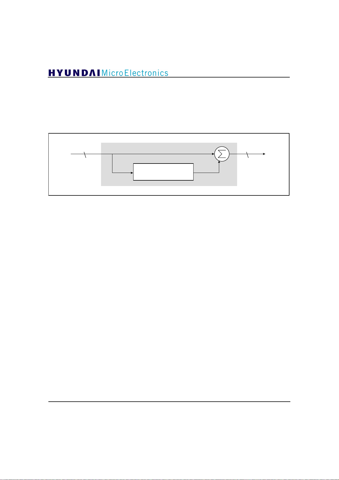
GDC21D003
6.3.10 NTSC Rejection
In the beginning of HDTV broadcasting, it will be
serviced with conventional NTSC broadcasting.
But in case that NTSC broadcasting exists in the
same channel where HDTV broadcasting is on the
air, at the HDTV signal’s point of view NTSC
10 10
Figure 6.3.15 Comb Filter Block
Figure 6.3.16 is the block diagram of NTSC
Rejection. PN511 signal section contained in Field
Sync helps to get MSE(Mean Square Error).
Difference(error) of input signal and reference
signal generated in Reference Generator is summed
during PN511 signal section and difference(error)
of input signal passed through Comb Filter and
reference signal passed through Comb Filter is
summed during PN511 section. These sums of
signal difference(error) are compared and the
smaller one is selected. The SNR of signal passed
through Comb Filter is decreased to 3dB low.
signal is interference. This interference is called as
co-channel interference. 3 carrier signals contained
in this co-channel interference can be removed by
using Comb Filter shown in Figure 6.3.15, but
should be checked first if there is co-channel
interference in current channel.
+
-
12 symbol delay
Therefore, if input signal has no co-channel
interference, the sum of error without passed
through Comb Filter is always smaller than the
other one that Comb Filter isn’t used. But if cochannel interference exists on channel, even though
the SNR of signal passed through Comb Filter is
3dB low, 3 carriers by co-channel interference are
removed. Therefore the signal passed through
Comb Filter has smaller sum than signal without
passed through Comb Filter and it is output as a
result.
48
Page 48
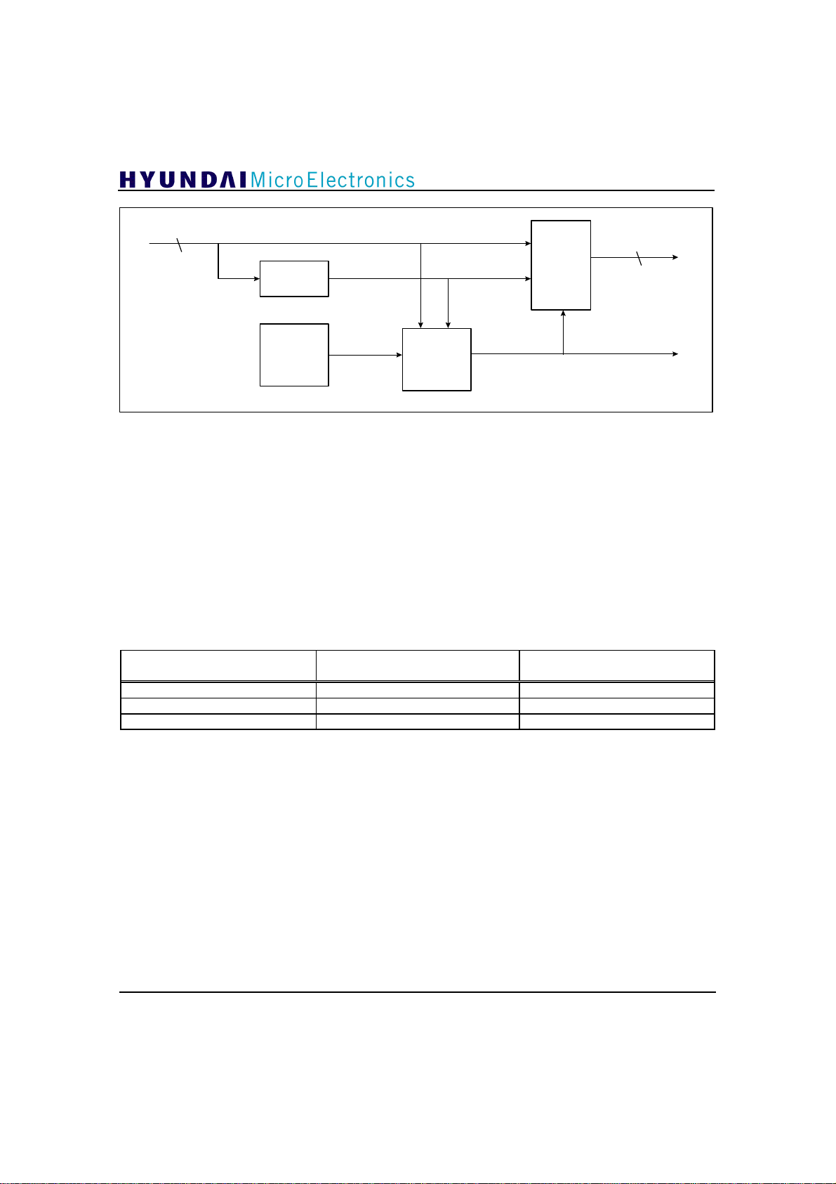
GDC21D003
10
Comb
Filter
Reference
Generation
Figure 6.3.16 The Block Diagram of NTSC Rejection
When NTSC co-channel interference is checked,
Comb Filter ON/OFF timing can be changed
through I2C bus. Its control signal is
NoCombgain[1:0](in I2C bus register5) and
controls this by changing error gain which doesn’t
use Comb Filter. When NoCombgain[1:0] is “00”,
gain is ‘1’. As a result, sum of error value during
PN511 section, which doesn’t use Comb Filter is
compared with the sum of the other during PN511
section, passed through Comb Filter. When it is
Table 6.3.5 Comb Filter Control through I2C Bus
MSE
&
Comparator
“01”, each error that doesn’ t use Comb Filter is
multiplied by the gain of ‘1.125’(1.023dB) and the
results are compared. When it is “10”, gain is
‘1.1875’ (1.493dB), and when “11”, gain is ‘ 1.25’
(1.983dB). By this manner, it is determined
whether Comb Filter will be used or not. The signal
to inform this to the next part is Combstat. And it
can be read through I2C bus. (in I2C bus register8)
Various controls can be done through I2C bus as
shown in Table 6.3.5.
10
Multiplexer
Combstat
NCombW
(in I2C bus register5)
‘1’ ‘ 1’ ‘ 1’ (Comb filter OFF)
‘1’ ‘ 0’ ‘0’(Comb filter ON)
‘0’ don’t care Internally detected signal
NComb
(in I2C bus register5)
Combstat
(in I2C bus register8)
49
Page 49
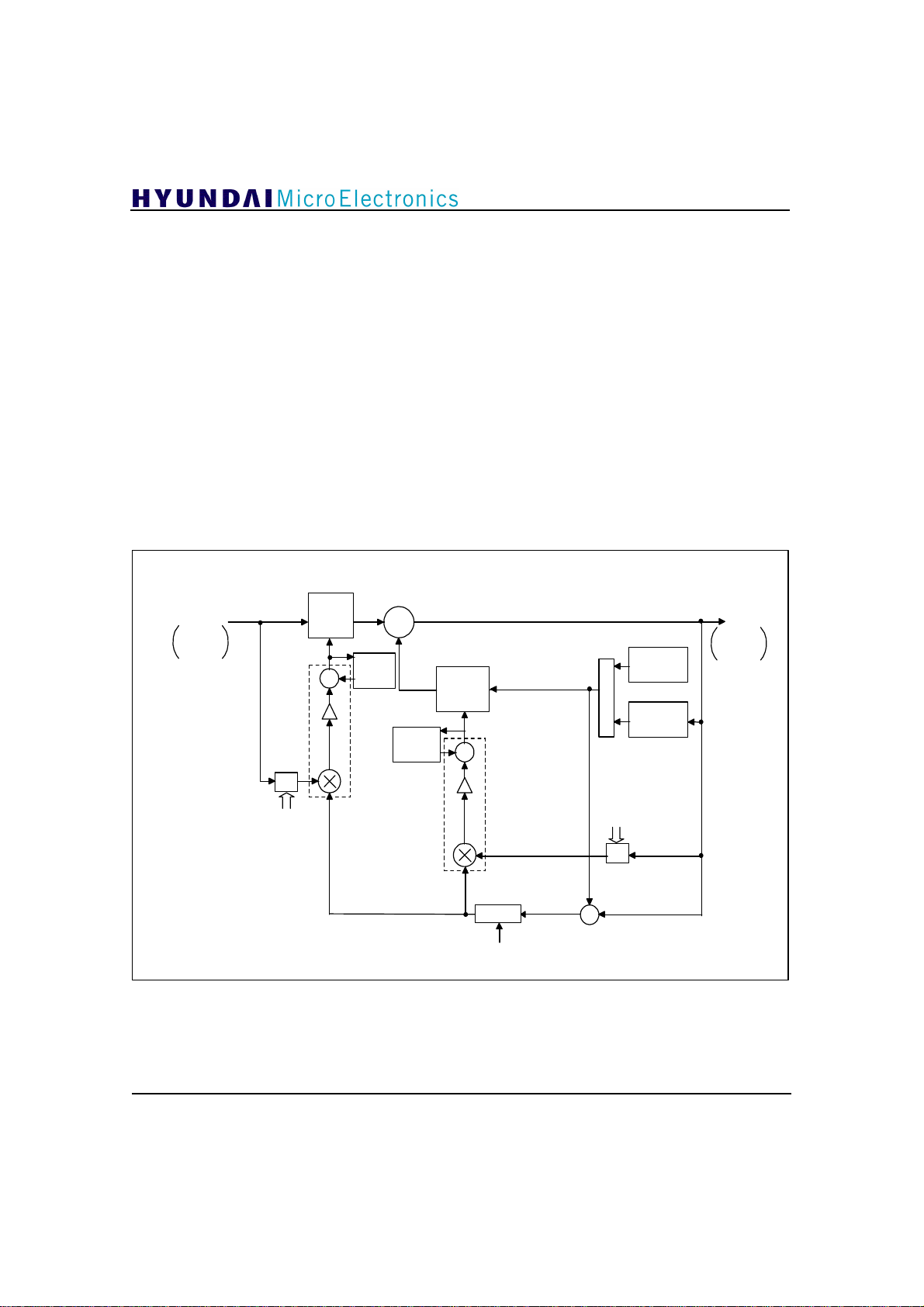
GDC21D003
6.4 Equalizer
The equalizer compensates for linear channel
distortions, such as tilt and ghosts. These
distortions can come from the transmission channel
or the imperfect components within the receiver.
The Equalizer uses a Least-Mean-Square algorithm
and decision feedback equalizer structure. The
adaptive equalization is performed with training
sequence, and blind equalization is also supported.
6.4.1 Block Diagram
The Equalizer has a decision feedback structure
with 64-tap feed-forward filter and 192-tap
feedback filter. Its internal diagram is Figure 6.4.1
and it consists of 256-tap adaptive filter, training
sequence generator, slicer, delays for data storage,
I Channel
Input
Symbols
10.76
MS/sec.
Forward
Tap Index
Filter
Taps
Delay 1
D
64 Tap
Forward
Filter
Σ
µ
+
Tap
Storage
Σ
-
Tap
Storage
Estimated
Error
192 Tap
Feedback
Filter
Filter
Taps
Σ
µ
subtractor, and control block. Each tap of 256-filter
tap has its own update part which is composed of
tap coefficient storage, adder, and multiplier. This
makes the equalizer converge into the channel
condition very fast. This filter is able to initialize
its coefficients through register33[2] (InitEQI2) bit
and update the coefficients internally during one
system clock(10.76 MHz) cycle as well as
download the coefficients through I2C register by
user. The outputs of feed-forward filter and
feedback filter are summed to produce the output.
This filter is applicable to 8 VSB terrestrial
broadcasting mode and 2, 4, 8, and 16 VSB cable
mode. Figure 6.4.2 shows the slicer of equalizer.
This decision feedback structure with a coefficient
update filter and LMS algorithm can optimize the
VSB equalizer in converging time, remaining error
and stability.
Equalized
I Channel
Output
10.76
Decision
Data
M
U
X
Feedback
Tap Index
D
Delay 2
Training
Sequence
Slicer
MS/sec.
-
Control
Σ
+
50
nFreezeEQ
Figure 6.4.1 Channel Equalizer
Page 50
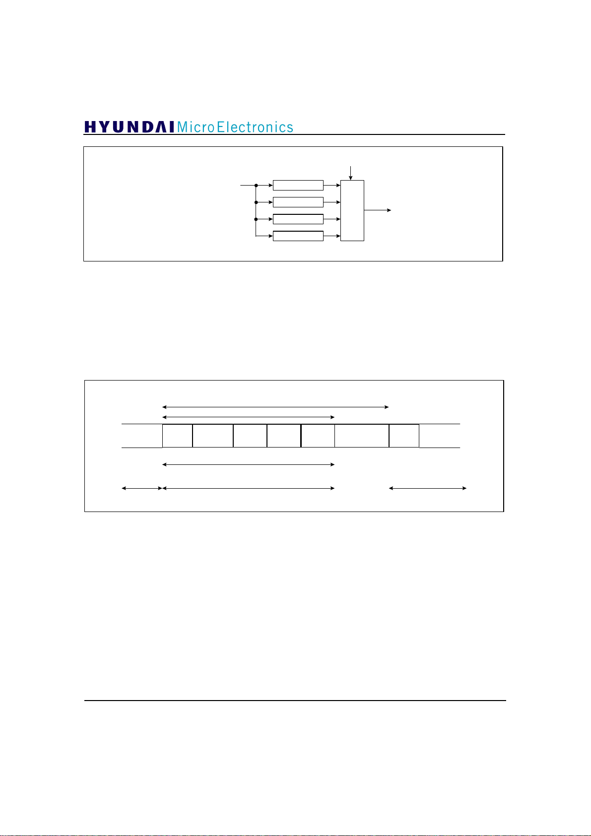
VSB mode
GDC21D003
Equalizer Output
Figure 6.4.2 VSB Slicer
6.4.2 Training/Data Mode Equalization
The Equalizer can achieve equalization through
three means: it can do adaptation on the binary
training sequence; it do adaptation on data symbols
throughout the frame when the eyes are open; or it
field interval
training sequence
data mode
equalization
Segment
sync
(4 symbols)
PN511
(511 symbols)
PN63
(63 symbols)
training sequence mode equalization
training sequence mode equalization data mode equalization
2VSB slicer
4VSB slicer
8VSB slicer
16VSB slicer
PN63*
(63 symbols)
MUX
Slicer Output
can do adaptation on data when the eyes are
closed(blind equalization). The principal difference
among these three methods is how the error
estimate is generated, and Figure 6.4.3 shows the
difference of training and data mode equalization.
PN63
(63 symbols)
...
Segment
sync
(4 symbols)
data ...data ...
Figure 6.4.3 Training/Data Equalization
51
Page 51
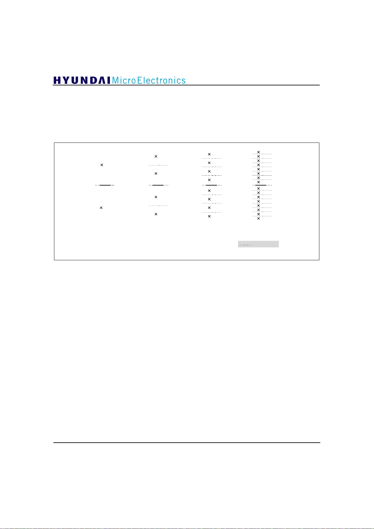
GDC21D003
6.4.3 Error Estimation
The Equalizer uses a Least Mean Square(LMS)
algorithm and can do adaptation on the transmitted
binary training sequences as well as on the
transmitted data. The LMS algorithm computes
4
-4
(a) 2VSB slice (b) 4VSB slice (c) 8VSB slice (d) 16VSB slice
Figure 6.4.4 VSB Slice Level
how to adjust the filter taps in order to reduce the
current error at the output of the Equalizer, by
generating an estimate of the current error in the
equalizer output signal using the slice level of
Figure 6.4.4.
6
7
5
2
3
1
-1
-2
-3
-5
-6
-7
15
13
11
9
7
5
3
1
-1
-3
-5
-7
-9
-11
-13
-15
: slice level
The estimated error is used in the adaptive filter to
update its coefficients as following equations.
One is for feed-forward adaptive filter and the
other is for feedback adaptive filter. The error is
1+
k
I
C
j
k
C
j
C
¥Ä
k
e
k
V
j
k
I
C
j
1+
k
C
j
C
¥Ä
k
e
^
k
I
j
+=
j
New j th filter tap coefficient of equalizer
1+
:
Current j th filter tap coefficient of equalizer
k
:
j
-sizestep
:
Current error value of equalizer
:
Current data stored in j th filter tap of Feedforward
:
+=
j
New jth filter tap coefficient of equalizer
:
Current jth filter tap coefficient of equalizer
k
:
j
-sizestep
:
Current error value of equalizer
:
Current decision data stored in jth filter tap of Feedback
:
¥Ä
¥Ä
kjkk
VeC
^1+
kjkk
IeC
52
multiplied by data and adjusted by step-size, and
then added to the stored coefficient value to get
new coefficient value.
Page 52
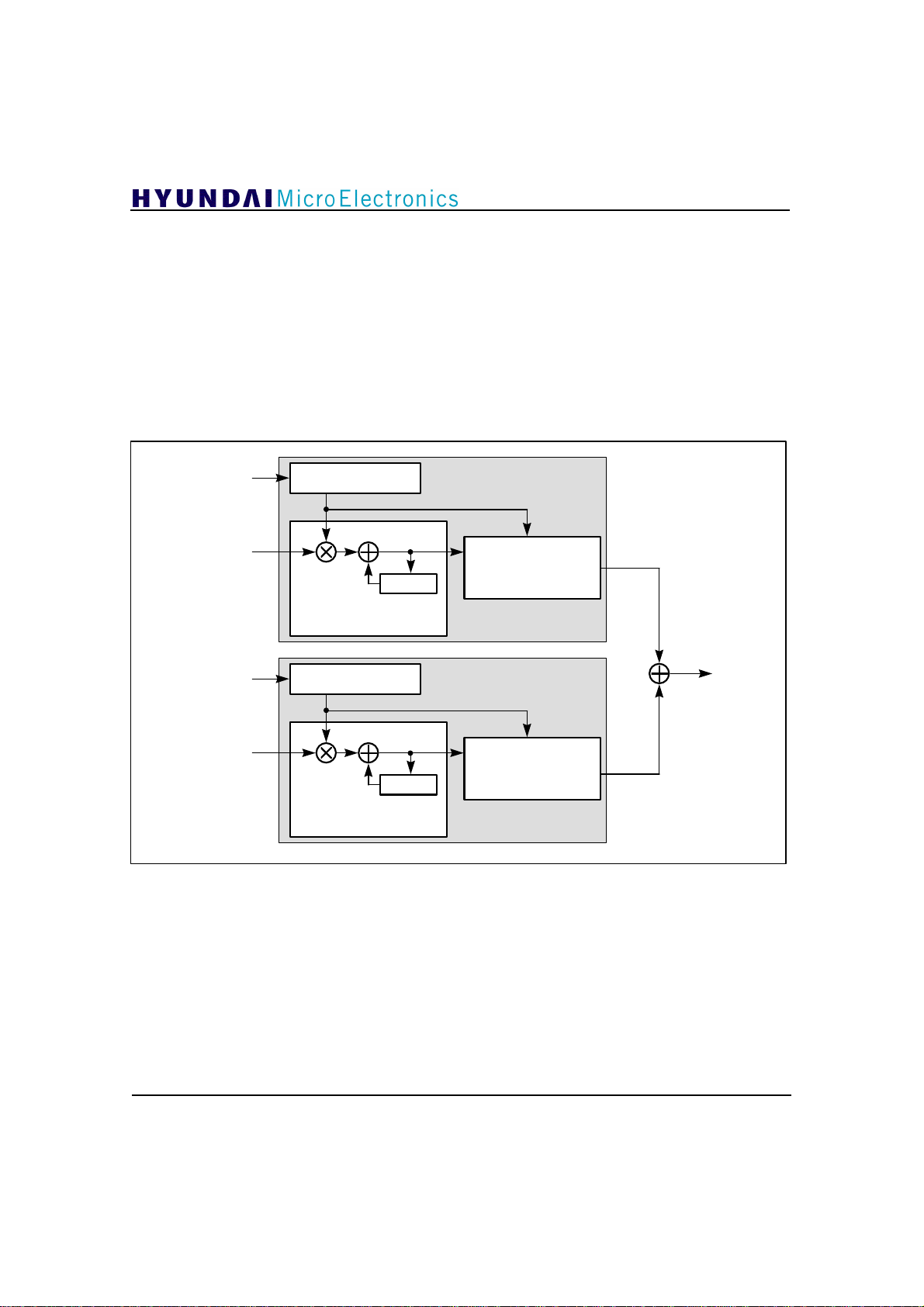
GDC21D003
6.4.4 Adaptive Filter
The 256-tap adaptive filter consists of two subfilters. One is feed-forward filter, and the other is
feedback filter. The feed-forward filter is 64-taps
long and the feedback filter is 192-taps long. The
data of feed-forward filter is I channel input
symbol. The data of feedback filter is training
sequence or sliced filter output. The coefficients
of this filter are updated internally by means of
the product of the estimated error by data delayed
in all taps. And the coefficients can be updated at
data
estimated error
decision data FLTout
Data Bank
Coefficient Bank /
Coefficient Updater
Data Bank 192-tap feedback filter
every clock. The multiplexing scheme can be
introduced for 4 taps to share one multiplier. The
number of multipliers is reduced to a quarter. The
products of data and coefficients are added and
accumulated to make output. The output of feedforward filter and the output of feedback filter are
summed to make the filter output. These outputs
are transferred to the phase tracker. And they are
used to calculate the estimated error with training
sequence and sliced filter output. Figure 6.4.5
shows the block diagram of the filter.
64-tap feedforward filter
Multiplier / Accumulator
memory
estimated error
memory
Coefficient Bank /
Coefficient Updater
Figure 6.4.5 Coefficient Update Filter
6.4.5 Equalizer Clock Scheme
The 256-tap filters are used in the equalizer.
Generally every tap has its own multiplier and the
portion of the multipliers is vast. The multiplexing
scheme can be introduced for several taps to share
one multiplier in this case. The 4-times
Multiplier / Accumulator
multiplexing scheme is used in our design.
Therefore one multiplier is shared to 4 taps. A
clock, 4-times multiplied by SYMCLK(symbol
clock) is needed for multiplexing. The PLL is used
for generating the 4-times multiplying
clock(CLK4EQ).
53
Page 53
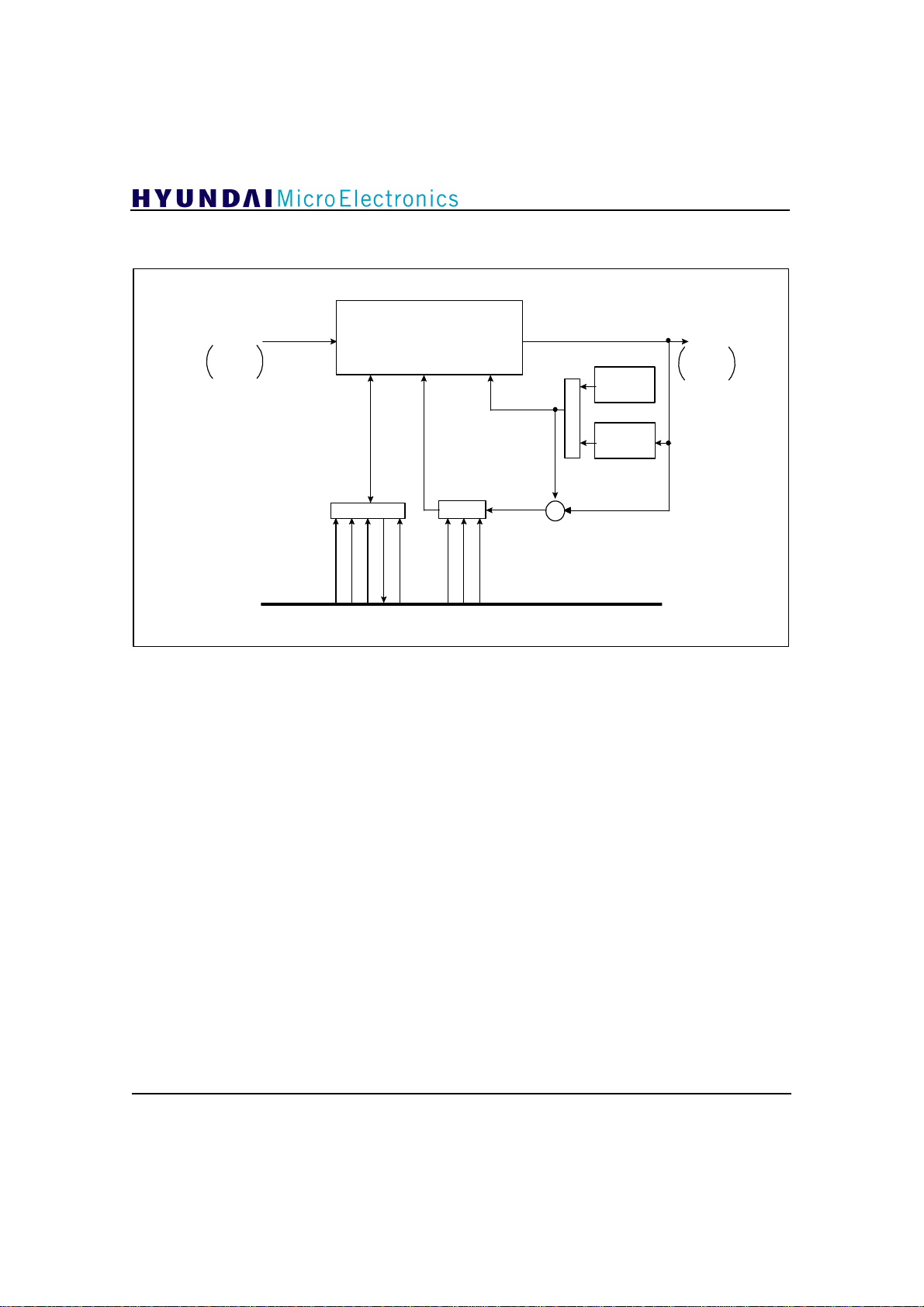
6.4.6 I2C Bus I/F
GDC21D003
I Channel
Input
Symbols
10.76
MS/sec.
256 tap adaptive filter
Coefficient
I2C Control
RdCoef
nCoefRead
nMakeRingEn
WrCoef
TAPaddress
Estimated Error
Figure 6.4.6 I2C Bus I/F
The adaptive filter is able to initialize and freeze its
coefficients through register33[2](InitEQI2) bit and
register33[3](nFreezeEQI2) bit. The control block
located at the front of filter controls the estimated
error value according to each operating mode and
sends it to the adaptive filter. These bits are in the
table 6.4.1. For example, if
register33[3](nFreezeEQI2) bit is set to “low”,
Equalizer Control block forces error value to be ‘0’,
which makes the coefficients of the filter
unchanged. The equalizer supports three different
Control
nInitEQ
nFreezeEQ
nAdtOnDataI2
Equalized
I Channel
Output
10.76
MS/sec.
M
U
X
Training
Sequence
Slicer
-
Σ
+
I2C BUS
step-sizes; the smallest, the middle, and the largest
step size. The difference is converging time and
remaining error. If the largest step-size is selected,
equalizer converges fast but the remaining error is
large. And if the smallest step-size is selected
equalizer converges slowly but the remaining error
is small. The decision directed mode can be used
for moving ghost by just setting nAdtOnDataI2.
When this signal is low, the decision directed
equalization is ON. When this pin is high, the
decision directed equalization is OFF.
54
Page 54
7 nFreezePHI2
6 InitPHI2
3 nFreezeEQI2
2 InitEQI2
[1:0]
STEPsizeIN
[1:0]
Table 6.4.1 Contents of I2C Bus Register33 for Equalizer
‘0’ : Freezes the Phase Tracker in the device, which means phase tracking does
not occur.
‘1’ : normal operation
W/R
If you want to control Phase Tracker fast, use external input pins.
Default value is ‘1’.
‘1’ : Initializes the Phase Tracker in the device.
‘0’ : normal operation
W/R
If you want to control Phase Tracker fast, use external input pins. Default value
is ‘0’.
‘0’ : Freezes the Equalizer in the device, which means coefficient update does
not occur.
‘1’ : normal operation
W/R
If you want to control Equalizer fast, use external input pins.
Default value is ‘1’.
‘1’ : Initializes the Equalizer in the device.
‘0’ : normal operation
W/R
If you want to control Equalizer fast, use external input pins.
Default value is ‘0’.
There are three available step-sizes in the Equalizer.
00,01 : smallest step size
10 : middle step size
W/R
11 : largest step size
Default value is “11”.
GDC21D003
The mean squared errors are calculated at equalizer
input and output, and these can be read by using
I2C bus. The location of center tap could be
changed using I2C bus, so the equalization range
Table 6.4.2 Contents of I2C Bus Register33 for Filter Control
‘0’ : feedback filter is on in 16 VSB mode
7 nIIR16ONIN
6 nIIRONIN
‘1’ : feedback filter is off
W/R
Default value is ‘1’.
‘0’ : feedback filter is on in 2, 4 and 8 VSB mode
W/R
‘1’ : feedback filter is on in only 8 VSB mode
Default value is ‘0’.
could be adjusted according to channel condition.
If you set nIIR16ONIN or nIIRONIN, the decision
feedback filter is turned off for 2, 4, and 16 VSB
mode.
55
Page 55

GDC21D003
6.4.7 Coefficient Reading/Writing
The adaptive filter is able to initialize and freeze its
coefficients as well as download the coefficients
through I2C register by user. The following are
coefficient reading/writing routines through I2C
register, and the I2C control block in figure 6.4.6
supports this coefficient reading/writing function
Equalizer / Phase Tracker Coefficient Write
Routine
1) Freeze an equalizer and a phase tracker.
(Sets nFreezeEQI2 and nFreezePHI2 to ‘0’)
2) Sets the nCoefRead to a write mode.
(set this bit to ‘1’)
3) Writes the filter tap address to write the
coefficients.(TapAddress : Register37)
4) Write the coefficients.
(WrCoef : Register38, 39)
5) Sets the nMakeRingIN to ‘0’.
6) Sets the nMakeRingIN to ‘1’.
7) To write another coefficients, goes to the 3rd step.
8) Sets nFreezeEQI2 and nFreezePHI2 to HIGH
and quits the write routine.
Equalizer Coefficient Read Routine
1) Freeze an equalizer and a phase tracker.
(Sets nFreezeEQI2 and nFreezePHI2 to ‘0’)
2) Set the nCoefRead to a read mode.
(Set this bit to ‘0’)
3) Writes the filter tap address to read the
coefficients. (TapAddress : Register37)
4) Set the nMakeRingIN to ‘0’.
5) Read the coefficients.(RdCoef : Register38, 40)
6) Set the nMakeRingIN to ‘1’.
7) To read another coefficients, goes to the 3rd step.
8) Set nFreezeEQI2 and nFreezePHI2 to HIGH and
quit the read routine.
6.5 Phase Tracker
The Phase Tracker corrects the untracked phase
noise in the receiver. It uses slice prediction
information that comes from the Viterbi Decoder
so that this phase tracker increases its performance
in severe noise environment. There are three loops;
gain correction loop, offset correction loop, and
phase correction loop. Phase Error Correction
block corrects the distortion caused by a phase
noise using an estimated error in the output of the
Phase Tracker.
User can control the gain of Phase Tracker by using
I2C register. There is a trade-off relation between
gain and noise enhancement in phase tracker. So
the phase tracker in this device change the gain
according to the noise condition. To increase the
performance the phase tracker is using the slice
predict information that comes from viterbi
decoder. Phase tracking range is -60° ~ 60° with
resolution of 0.004°. This means that phase error
estimation part can estimate phase error degree
with 0.004° resolution and phase tracker can track
the phase noise from -60° to 60° successfully. A
block diagram of the Phase Tracker is shown in
Figure 6.5.1.
56
Page 56
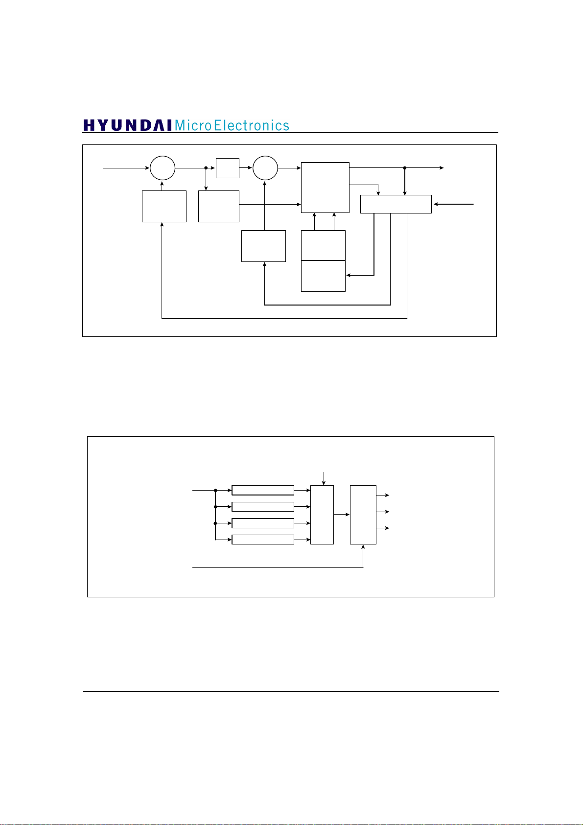
GDC21D003
I
(input)
Gain
X
Accumulator
Limiter
Delay
Hilbert
Transform
Filter
Accumulator
Gain Error
Figure 6.5.1 Phase Tracker
6.5.1 Error Detection
The result I signal is output to channel decoder and
used at error detection with result Q signal to get
estimated phase error degree. Figure 6.5.2 shows
the block diagram of error detection. Result
Offset
+
Limiter
I’
Q’
Offset Error
I
(output)
Slice Prediction
from
Viterbi Decoder
Derotator
cos sine
Sine
Cosine
Table
Accumulator
Limiter
I ”
Q”
Error Decision
Phase
Error
I signal is input to VSB mapper which is a Look-up
table and the output of this look-up table is a kind
of decision error. The 2nd Look-up Table converts
decision error to gain error, offset error, and phase
error. And these error information are accumulated
and used to remove phase noise.
I”
Q”
VSB mode
2VSB mapper
4VSB mapper
MUX
8VSB mapper
16VSB mapper
Figure 6.5.2 Error Detection
Error
Lookup
Table
Gain Error
Offset Error
Phase Error
57
Page 57
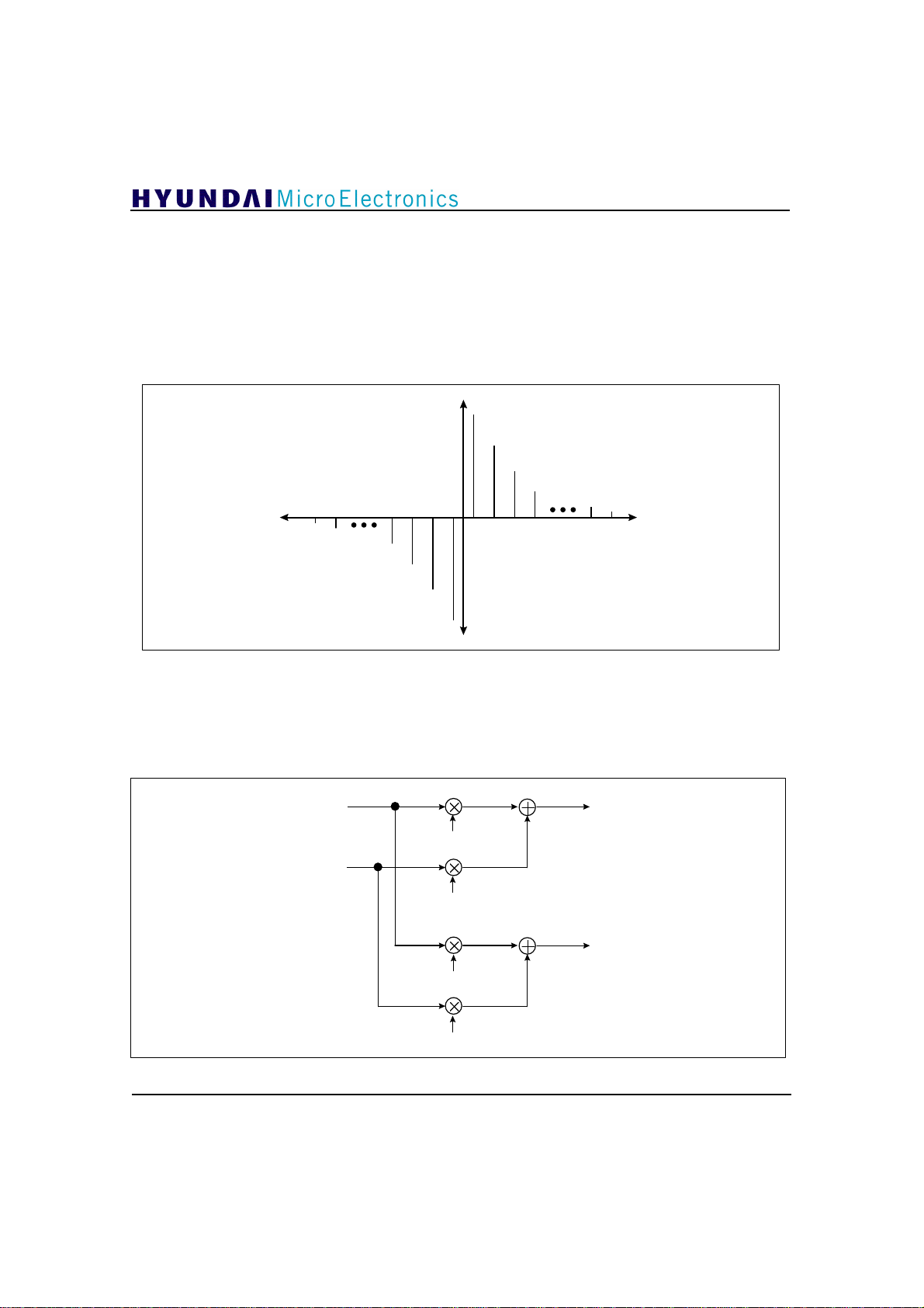
GDC21D003
6.5.2 Gain & Offset Loop
There are three loops in phase tracker and these
loops are designed to be ON/OFF through I2C bus.
The first loop is Gain Loop. The Gain Loop
consists of multiplier and accumulator, and corrects
gain error caused by phase error with error value
from an error decision. The output of equalizer is
the first gain controlled by a multiplier. The second
Figure 6.5.3 Coefficients of Hilbert Transform Filter
loop is Offset Loop which consists of adder and
accumulator. The Offset Loop corrects offset error
caused by phase error with error value from an
error decision. The gain-corrected output is used to
remove offset error at Offset Loop and used at the
Hilbert transform filter to generate an
approximation of the Q signal. Figure 6.5.3 shows
the shape of coefficients of Hilbert Transform filter.
amplitude
time
6.5.3 Phase Loop
The last loop is Phase Loop which consists of adder,
accumulator, Sine Cosine Table, and Complex
I’
Q’
Figure 6.5.4 Complex Multiplier
58
Multiplier. The gain & offset of corrected I and Q
signal is derotated at complex multiplier to correct the
phase error and Figure 6.5.4 shows the diagram of
complex multiplier for a derotation.
cos
sine
sine
cos
+
-
+
+
I”
Q”
Page 58
GDC21D003
6.5.4 I2C Bus I/F
User can initialize the resulting phase tracking
value through I2C register33[6] (InitPHI2) bit.
There are three loops in phase tracker; gain
correction loop, offset correction loop, and phase
Table 6.5.1 Contents of I2C Bus Register33 for Phase Tracker
‘0’ : Freezes the Phase Tracker in the device, which means phase tracking does
not occur.
7 nFreezePHI2
6 InitPHI2
PHASmodeIN
[5:4]
[1:0]
There are 4 different modes for phase tracking gain
control as seen in the table 6.5.2. There is a tradeoff relation between gain and noise enhancement in
phase tracker. So the phase tracker in this device
changes the gain according to the noise condition.
As shown in table, if LOOPgainIN is set to “000”
gain is changed automatically according to the
‘1’ : normal operation
W/R
If you want to control Phase Tracker fast, use external input pins.
Default value is ‘1’.
‘1’ : Initializes the Phase Tracker in the device.
‘0’ : normal operation
W/R
If you want to control Phase Tracker fast, use external input pins.
Default value is ‘0’.
There are three loops in the Phase Tracker, gain, offset, and phase loop.
00 : all loops on
01 : offset loop off
W/R
10 : offset and gain loops off
11 : all loops off
Default value is “00”.
correction loop. The following table shows
contents of register address 33 and these three
loops can be turned on/off through this
register[5:4] (PHASmodeIN). The mean squared
errors are calculated at phase tracker output and
can be read using I2C bus through MeanErrOUTPH.
noise condition. This means that this routine has
noise calculator and selects a gain by using the
calculated noise information. User can also control
the gain of phase tracker by setting to “001”, “010”,
or “011”. The default is “000” with this automatic
gain mode.
[5:3]
LOOPgainIN
[2 : 0]
Table 6.5.2 Contents of I2C Bus Register36 for Gain Control
Determines the use of automatic gain routine and the type of loop gain used in
Phase Tracker. Default value is “000”.
“000” : Automatic gain change.
“001” : phase tracker is OFF.
W/R
“010” : smaller gain.
“011” : normal gain.
“1xx” : not use.
59
Page 59
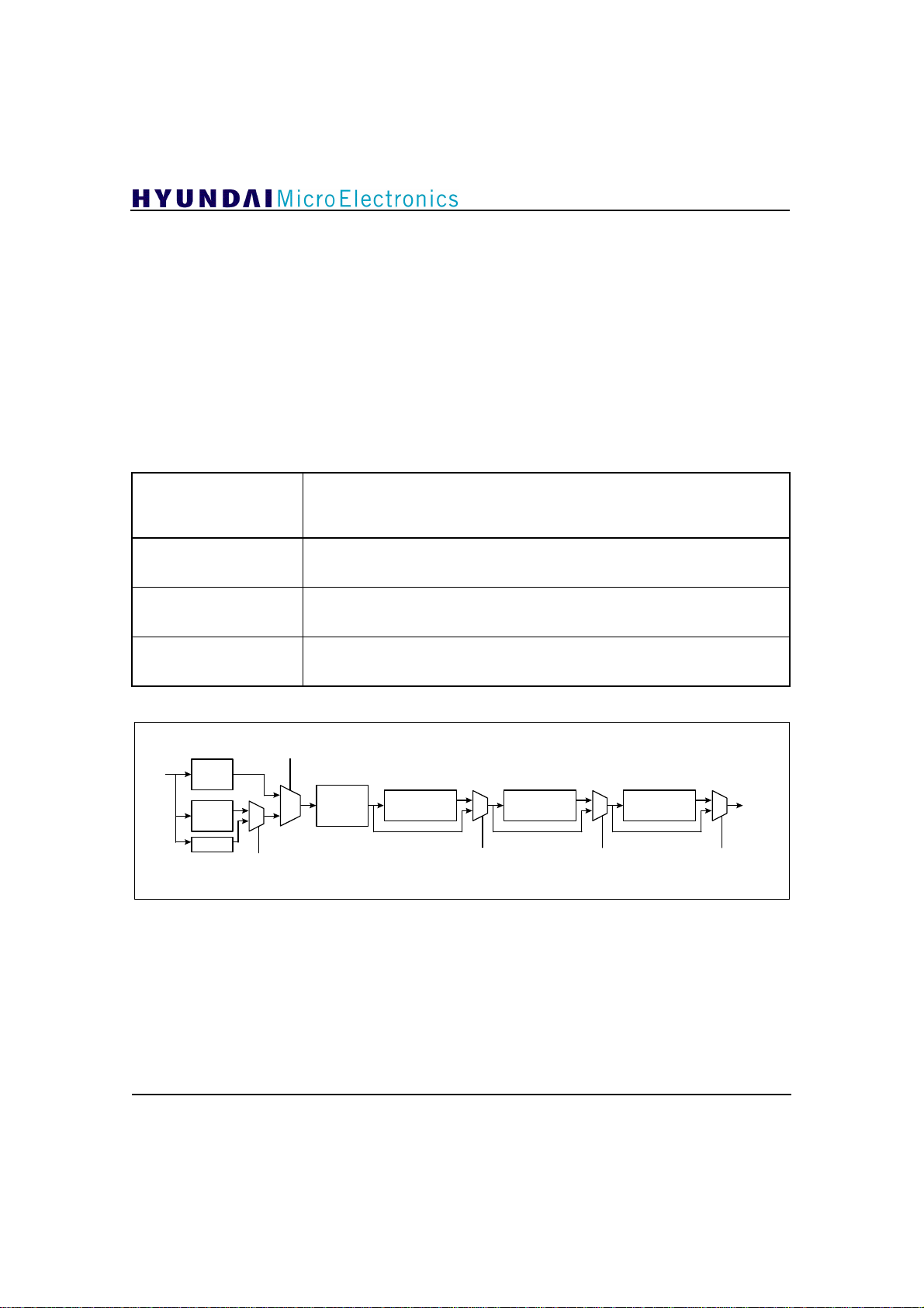
GDC21D003
6.6 Channel Decoder
Channel Decoder consists of Cable Slicer, Viterbi
Decoder, Symbol-to-Byte Converter,
Convolutional Deinterleaver, Reed-Solomon
Decoder, Data Derandomizer, Transport
Demultiplexer Interface, and etc. as shown in
Figure 6.6.1. Channel Decoder input comes from
Phase Tracker. MMDS 2/4/8/16 VSB signal and
ATSC 16 VSB signal are sliced in Cable Slicer,
and ATSC 8 VSB signal is decoded in Viterbi
Decoder. Viterbi Decoder is bypassed when I2C
Table 6.6.1 I2C bus register64 values for sub-block bypass
Viterbi Decoder on/off selection
Viterbi_on
Deint_on
RSdec_on
Derand_on
‘1’ : on ‘ 0’ : off
If this bit is set to ‘0’, hard decision decoding is performed instead of viterbi
decoding. Default value is ‘1’.
Deinterleaver on/off selection
‘1’ : on ‘ 0’ : off
If this bit is set to ‘0’, deinterleaver is bypassed. Default value is ‘ 1’ .
RS Decoder on/off selection
‘1’ : on ‘ 0’ : off
If this bit is set to ‘0’, RS decoder is bypassed. Default value is ‘ 1’ .
Derandomizer on/off selection
‘1’ : on ‘ 0’ : off
If this bit is set to ‘0’, derandomizer is bypassed. Default value is ‘ 1’ .
register64[7](Viterbi_on) value is ‘0’. In this case,
signal is sliced by 4-level slicer. Symbol stream,
the output of Cable Slicer and Viterbi Decoder is
converted into Byte Stream by Symbol-to-Byte
Converter and sent to Convolutional Deinterleaver.
Convolutional Deinterleaver is bypassed when I2C
register64[6] (Deint_on) value is ‘0’. ReedSolomon Decoder and Data Derandomizer are
bypassed when I2C register64[5] (RSdec_on) and
I2C register64[4] (Derand_on) are set to ‘0’
respectively. I2C register values bypassing each
block are shown in Table 6.6.1.
60
Phase
Tracker
Cable
Slicer
Viterbi
Decoder
Slicer
Vsbmode
1
0
Viterbi_on
Symbol-
to-Byte
Converter
Convolutional
Deinterleaver
1
0
Deint_on
Reed-Solomon
Decoder
1
0
RSdec_on
Figure 6.6.1 Block Diagram of Channel Decoder
Data
Derandomizer
Transport
Demultiplexer
I/F
1
0
Derand_on
Page 60
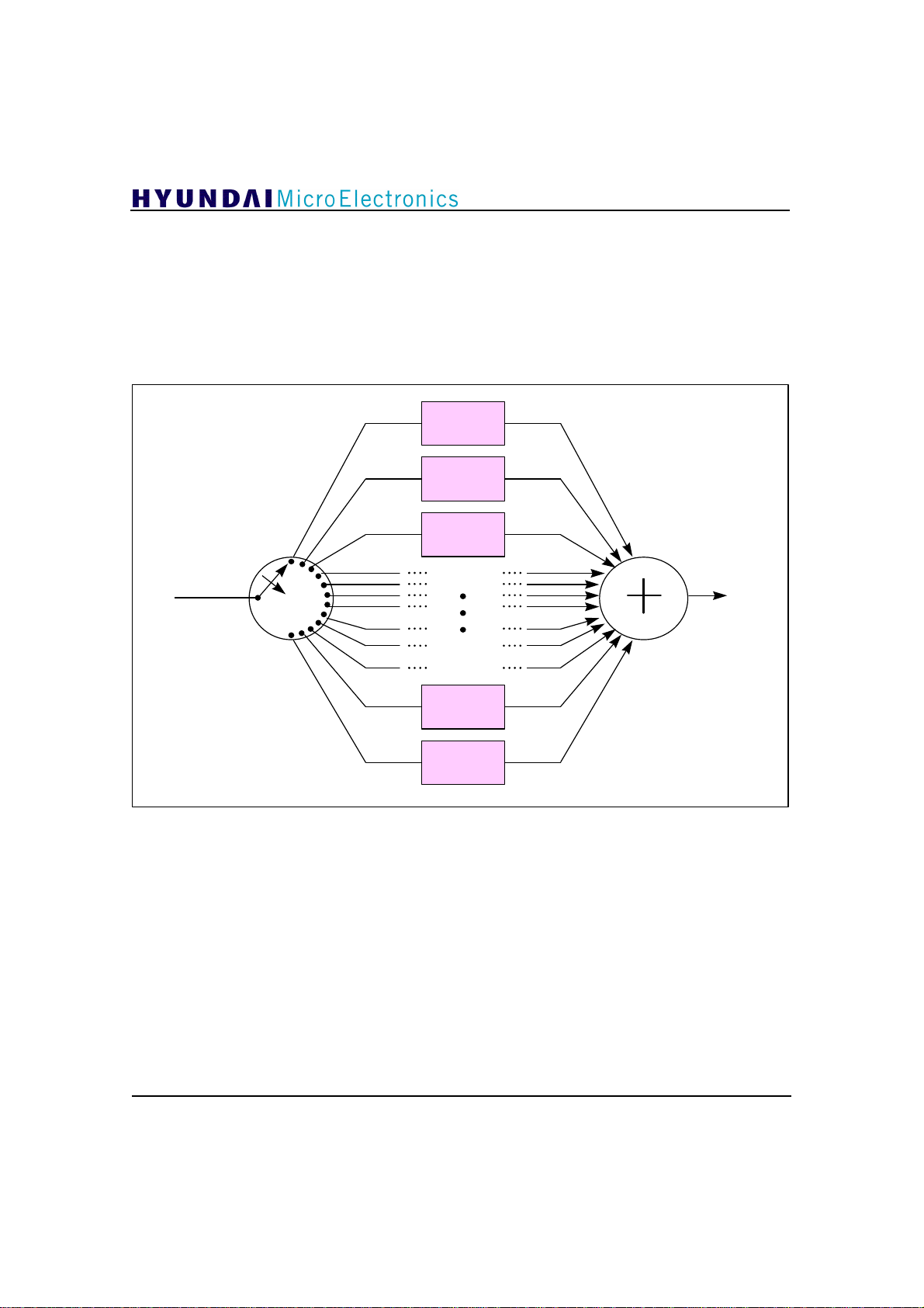
GDC21D003
6.6.1 12 Symbol Intrasegment
Deinterleaver
To help protect the Viterbi decoder against short
burst interference, such as impulse noise or NTSC
co-channel interference, 12-symbol code
intrasegment interleaving is employed in the
transmitter. As shown in figure 6.6.2, the Viterbi
Equalized &
Phase Corrected
Symbols
decoding block uses 12 Viterbi decoders in parallel,
where each Viterbi decoder sees every 12th symbol.
This code interleaving has all the same burst noise
benefits of a 12-symbol interleaver, but also
minimizes the resulting code expansion when the
NTSC rejection comb filter is active (when the
NTSC rejection comb filter is active, the I2C
register8[4](Ncomb) is set to ‘0’).
Viterbi Decoder
#0
Viterbi Decoder
#1
Viterbi Decoder
#2
Viterbi
Decoded
Data
Figure 6.6.2 12 Symbol Intrasegment Deinterleaver
6.6.2 Segment Sync Suspension
Before the 8 VSB signals can be processed by the
Viterbi decoder, it is necessary to suspend the
Segment Sync. The presence of the Segment Sync
character in the data stream passed through the
comb filter presents a complication that must be
dealt with, because Segment Sync is not trellis
encoded or precoded. Figure 6.6.3 shows the
technique that has been used. It shows the receiver
processing that consists of the comb filter in the
VSB Synchronizer/Equalizer and Segment Sync
Removal block in this chip. The multiplexer in the
Segment Sync Removal block is normally in the
Viterbi Decoder
#10
Viterbi Decoder
#11
upper position. This presents data that has been
filtered by the comb filter to the Viterbi Decoder.
However, because of the sync character in the data
stream, the multiplexer selects its lower input
during the 4 symbols that occurs 12 symbols after
the Segment Sync. The effect of this sync removal
is to present to the Viterbi Decoder a signal that
consists of the subtraction of two adjacent data
symbols that come from the same Viterbi Decoder,
one transmitted before and one after the Segment
Sync. The interference introduced by the Segment
Sync symbol is removed in this process, and the
overall channel response seen by the Viterbi
Decoder is the single-delay partial response filter.
61
Page 61
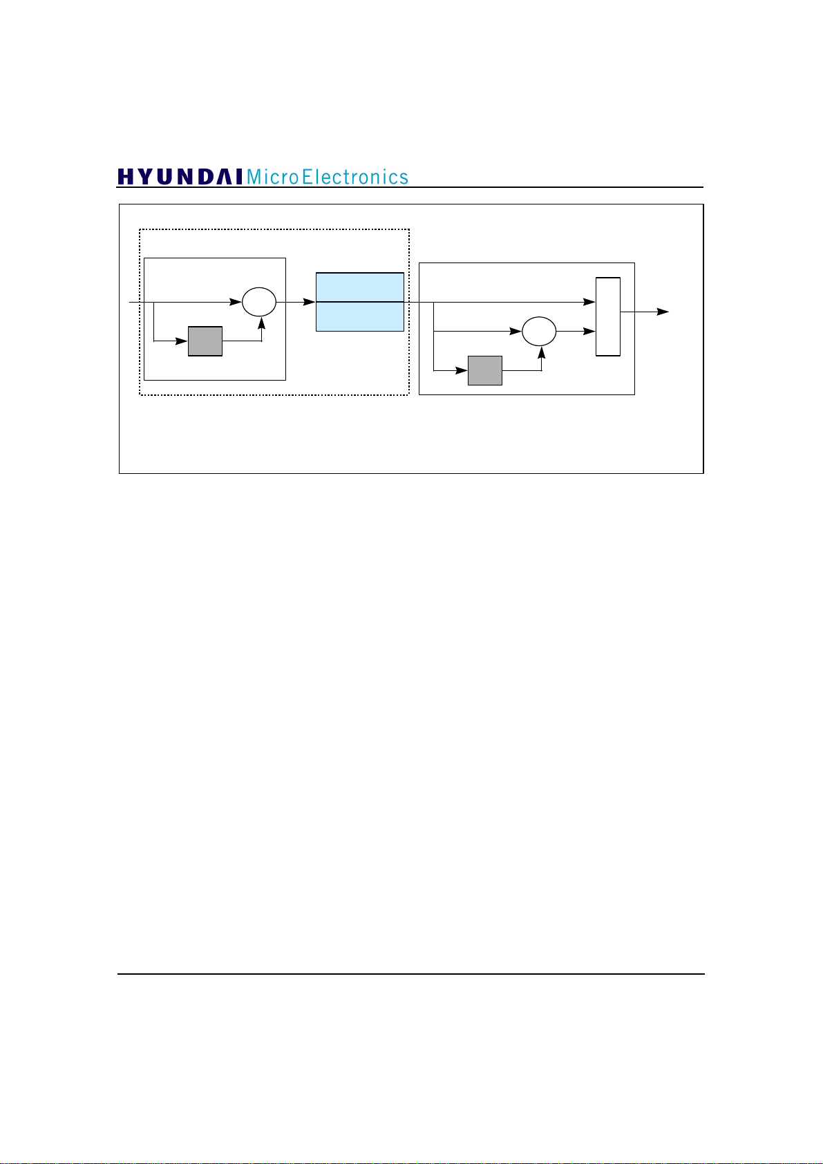
Comb Filter Segment Sync Removal
GDC21D003
Equalizer
¢²
£-
Phase Tracker
D
VSB Synchonizer/Equalizer
Figure 6.6.3 Segment Sync Suspension
6.6.3 Viterbi Decoder
The Viterbi decoder performs the task of slicing
and convolutional decoding. It has two modes; one
is for the case when the NTSC rejection filter is
used to minimize NTSC co-channel, and the other
is when it is not used. This is illustrated in Figure
6.6.4. The insertion of the NTSC rejection filter is
determined automatically in the comb filter control
block(before the equalizer, see Figure 6.6.3), with
this information passed to the Viterbi decoder .
When there is little or no NTSC co-channel
interference, the NTSC rejection filter is not used
and an optimal Viterbi decoder is used to decode
the 4-state trellis-encoded data. Serial bits are recreated in the same order as they were created in
the encoder. With significant NTSC co-channel
interference, if the NTSC rejection filter(12 symbol,
feed-forward subtractive comb) is employed, an
optimized 8-state Viterbi decoder for this partial
response channel is used. The Viterbi decoder can
be bypassed for performance tests by setting I2C
register64[5](Viterbi_on) to ‘0’. Then, just 4-level
slicing is done. Also, on ATSC 16 VSB and
MMDS 2/4/8/16 VSB mode, the Viterbi decoder is
bypassed and only slicing is done. Figure 6.6.5 is
internal block diagram of Viterbi decoder. Each
branch metric of trellis calculated in branch metric
D
(D = 12 Symbols Delay)
block is 6bits, memory depth of path memory
block is 16. Branch metric block and ACS(Add,
Compare, and Select) block are adapted to be 4state Viterbi decoder if I2C register84[4](Ncomb)
value is ‘1’, or 8-state Viterbi decoder if it is ‘ 0’ .
12 Vitervi decoders are implemented through 12
shift registers sharing one Branch metric block and
one ACS block.
¢²
M
U
X
to
Viterbi
Decoder
62
Page 62
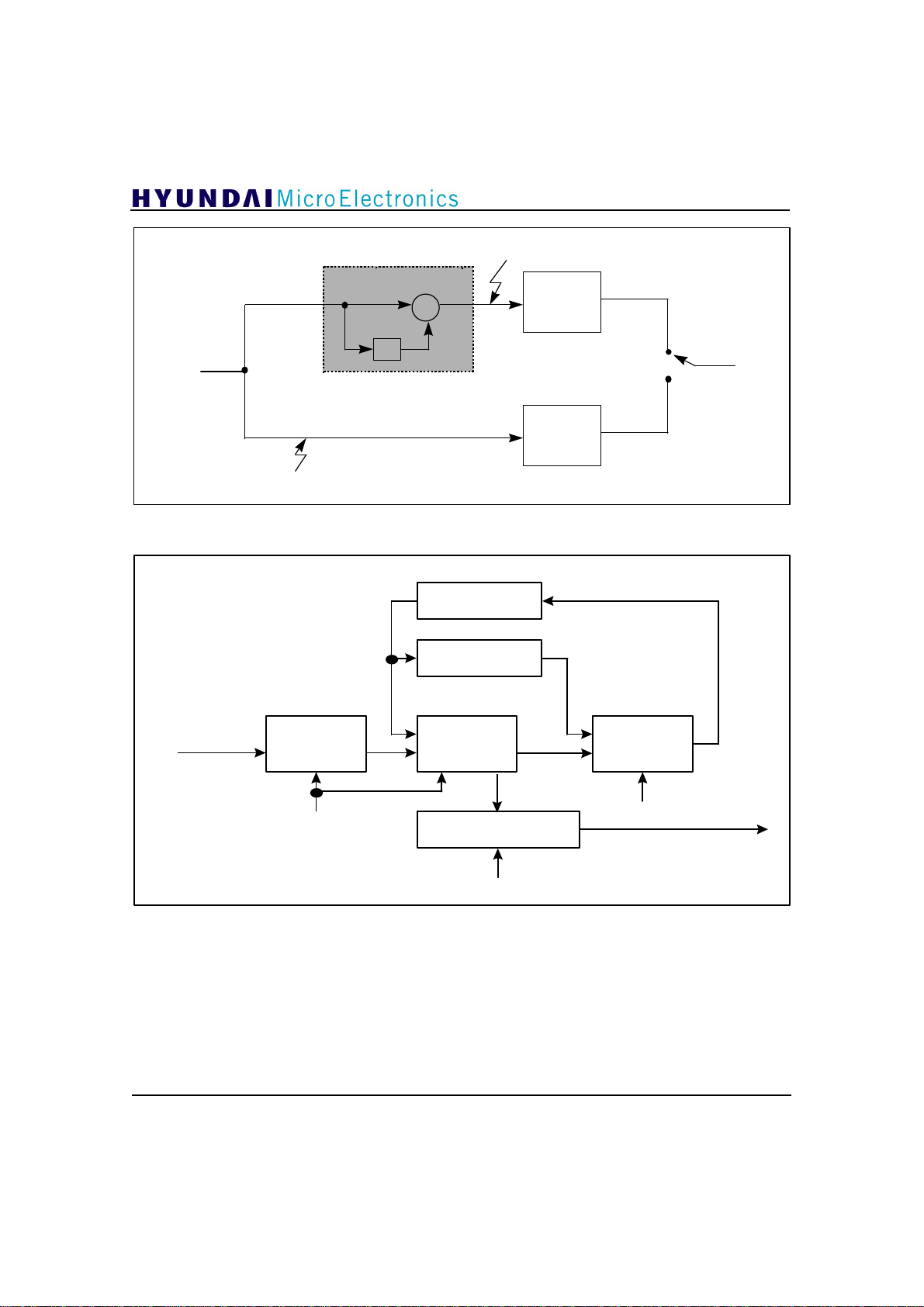
NTSC Rejection Filter
¢²
GDC21D003
15 Level Symbols
+ Noise + Interference
Partial
Response
Viterbi
Decoder
Received
Symbols
From
Segment Sync
Suspension
D
(D = 12 Symbols Delay)
Optimal
Viterbi
Decoder
8 Level Symbols
+ Noise + Interference
Figure 6.6.4 Viterbi Decoding with and without NTSC Rejection Filter
Shift
Register1
Shift
Register2
Branch
Metric
ACS
MUX
Sync
Ncomb
Path Memory
Symbol-to-byte
Sync
Converter
Data
Out
To
Figure 6.6.5 Internal Block Diagram of Viterbi Decoder
63
Page 63
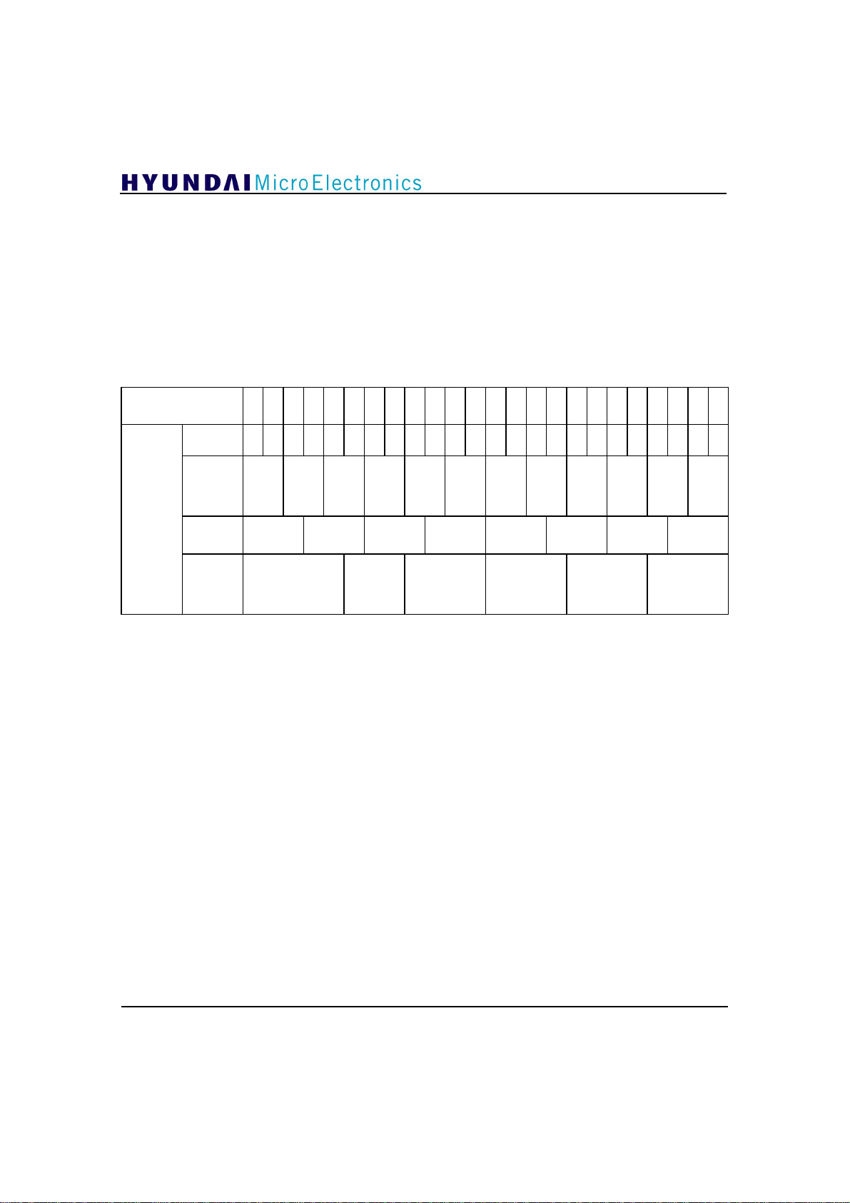
GDC21D003
6.6.4 Symbol-to-Byte Converter
The symbol-to-byte converter converts
incoming symbols to bytes. On MMDS 2 VSB
mode, each received symbol has one bit of data.
The data from MSB to LSB {7,6,...,1,0}is entered
and 8 symbols compose one byte. On MMDS 4
VSB and ATSC 8 VSB mode, each received
symbol has two bits of data. The data from MSB to
Table 6.6.2 Symbol-to-Byte Conversion
Bits in Byte 7 6 5 4 3 2 1 0 7 6 5 4 3 2 1 0 7 6 5 4 3 2 1 0
Symbol
MMDS
2VSB
MMDS
4VSB/
ATSC
8VSB
MMDS
8VSB
MMDS
16VSB/
ATSC
16VSB
0 1 2 3 4 5 6 7 0 1 2 3 4 5 6 7 0 1 2 3 4 5 6 7
0 1 2 3 0 1 2 3 0 1 2 3
0 1 2 3 4 5 6 7
0 1 0 1 0 1
LSB {76,54,32,10} is entered and 4 symbols
compose one byte. On MMDS and ATSC 16 VSB
mode, each received symbol has four bits of data.
The data from MSB to LSB {7654,3210} is entered
and 2 symbols compose one byte. On MMDS 8
VSB mode, each received symbol has three bits of
data. The data from MSB to LSB
{765,432,107,654,321,076,543,210} is entered and
8 symbols compose three bytes. See Table 6.6.2
64
Page 64
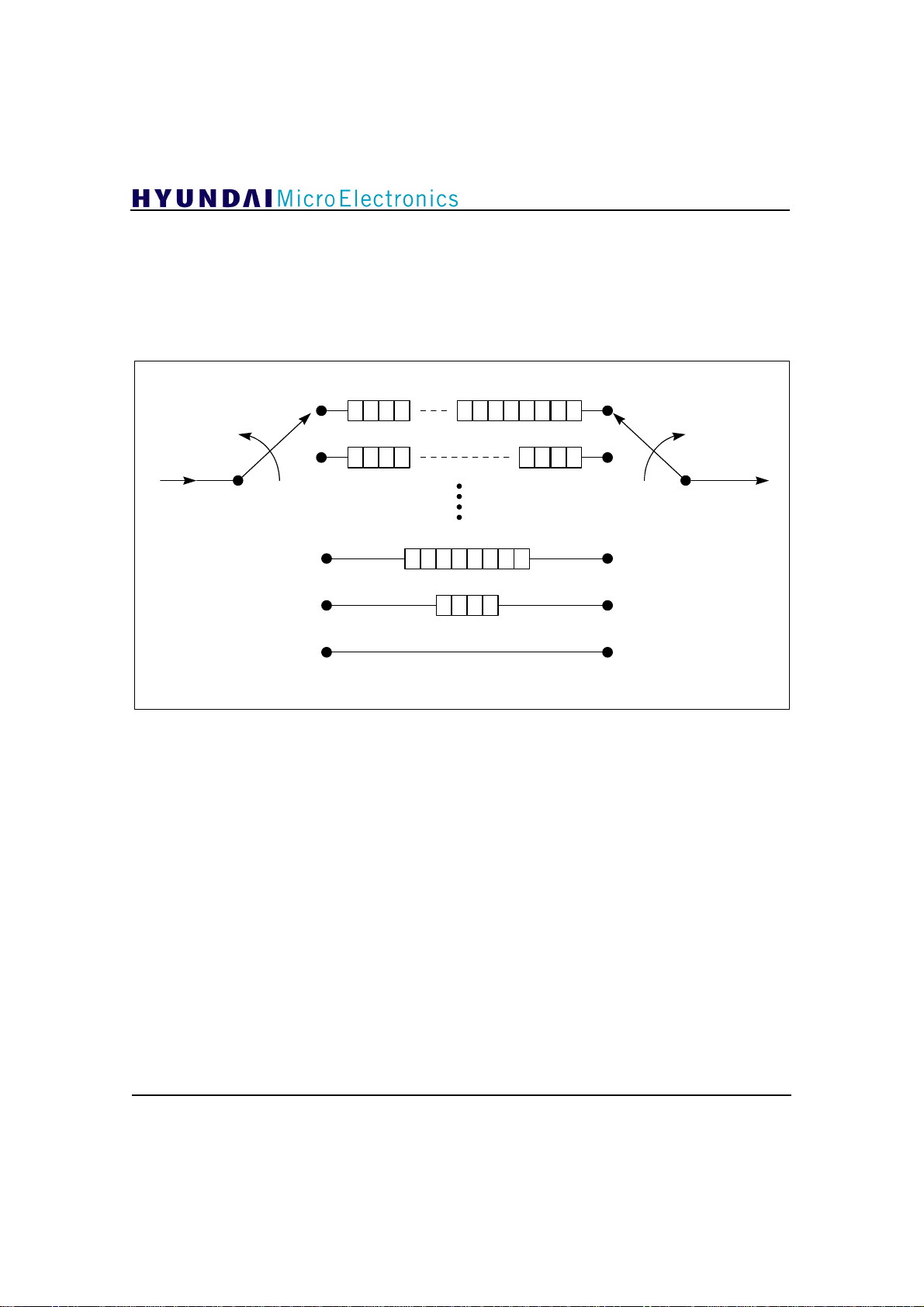
GDC21D003
(
)
6.6.5 Convolutional Deinterleaver
Convolutional deinterleaver performs the opposite
function of the transmitter convolutional
interleaver. Even strong NTSC co-channel signals
passing through the NTSC rejection filter and
creation of short bursts due to NTSC vertical edges
1
2
From
Symbol-to-Byte
Converter
50
51
(B=)52
M=4, B=52, N=208, R-S Block = 207,B¡¿M=N
are reliably handled due to the interleaving and RS
coding process. The deinterleaver uses Data Field
Sync for synchronizing with the first data byte of
the data field. The structure is shown in Figure
6.6.6. The deinterleaver can be bypassed for
performance tests by setting I2C register64[5]
(Deint_on) to ‘0’.
(B-1)M
(B-2)M
To
Reed-Solomon
Decoder
2M
M (=4 Bytes)
Figure 6.6.6 Convolutional Deinterleaver
6.6.6 Reed-Solomon Decoder
and RS error correction. The RS decoder can be
turned off for performance test by setting the I2C
Reed-Solomon decoder can correct up to 10byte errors per Data Segment that is encoded by
RS(207, 187) code. Any burst errors created by
impulse noise, NTSC co-channel interference, or
Viterbi decoding errors, are greatly reduced by the
combination of the convolutional deinterleaving
G X X X X X X X X X X X
20 19 18 17 16 15 14 13 12 11
= + + + + + + + + +
+ + + + + + + + + + +
152 185 240 5 111 99 6 220 112
10 9 8 7 6 5 4 3 2 1
X X X X X X X X X X
150 69 36 187 22 228 198 121 121 165 174
register64[4](rsdec_on) to ‘0’. The number of
segment errors per one second is written in I2C
register65 and register67 so that they can be read
through I2C register control. The encoder
polynomial is as follows. The coefficients of the
polynomial are defined in Galois field GF(256).
65
Page 65
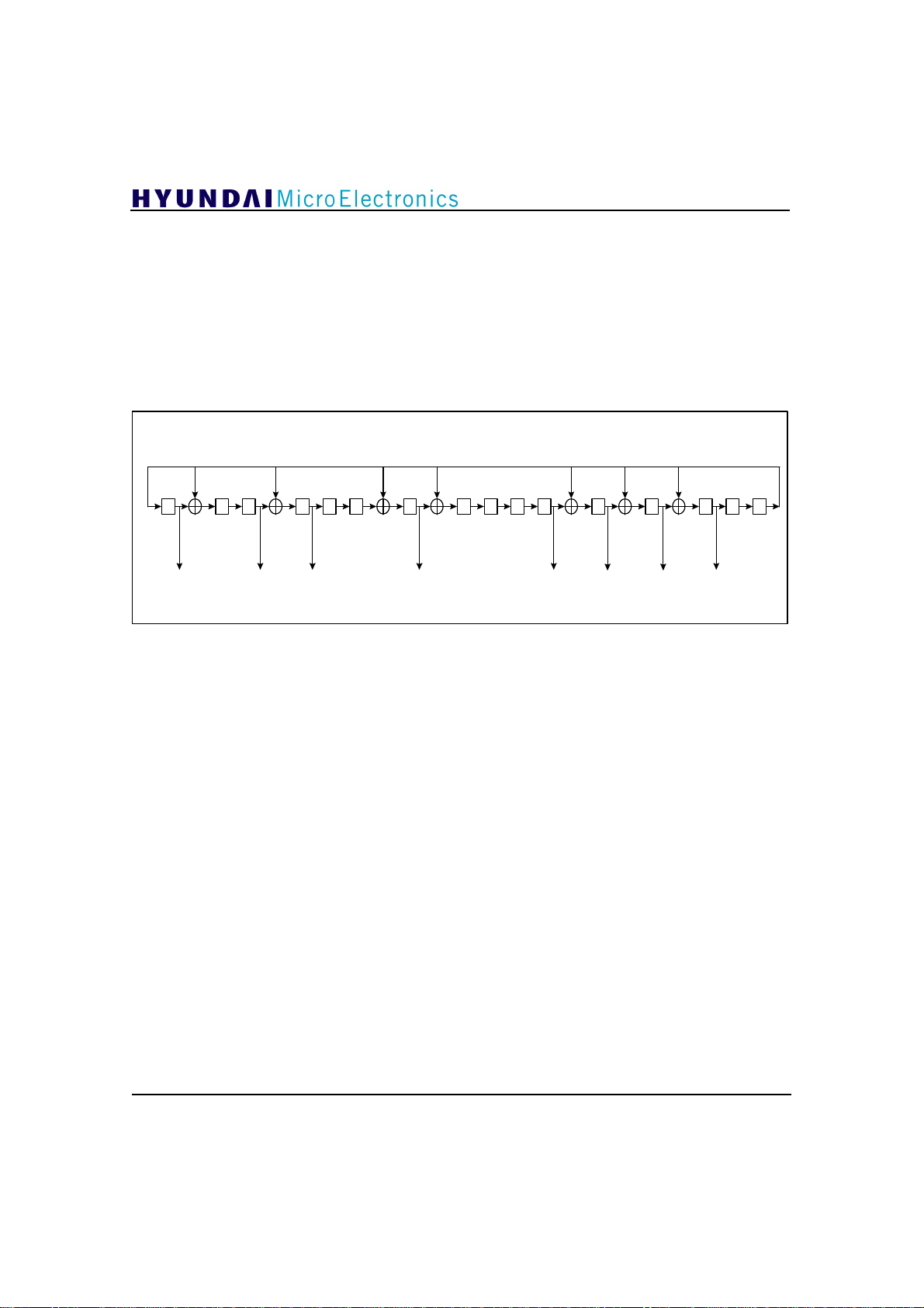
GDC21D003
6.6.7 Data Derandomizer
The data(excluding Field Sync Data, Segment Sync
Data, and parity bytes) is randomized at the
transmitter by Pseudo Random Sequence(PRS).
The de-randomizer accepts the error-corrected data
bytes from the RS decoder, and applies the same
PRS randomizing code to the data. The PRS code
is generated identically as in the transmitter, using
the same PRS generator feedback and output taps
2
2
X
X
0
D
X
4
X
1
D
D
6
5
X
X
2
Figure 6.6.7 Derandomizer Polynomial
as shown in Figure 6.6.7. Since the PRS is locked
into the reliably recovered Data Field Sync(and not
some code words embedded within the potential
noisy data), it is exactly synchronized with the data
and performs reliably. The initialization(pre-load)
to F180H occurs during the Data Segment Sync
interval prior to the first Data Segment. The data
derandomizer can be bypassed for performance
tests by setting the I2C register64[3](Derand_on) to
‘0’.
7
X
D
8
X
3
X9X
10
X
D
11
12
X
4
D
13
X
5
6
D
15
14
X
16
X
X
7
D
66
Page 66
6.6.8 I/F to Transport Demultiplexer
GDC21D003
The VSB Channel Decoder offers various functions
for the interface with the Transport Demultiplexer
which are controlled by I2C register64.
Table 6.6.3 I2C Register64 Flags controlling Transport Demultiplexer I/F
Parallel/serial output selection
‘1’ : parallel ‘ 0’ : serial
Pase
Derand_on
Errorflag_ins
Vsbdvalid_pol
Vsbclk_sup
If this bit is set to ‘0’, VSBDATA[0] pin is used as serial data output and
VSBDATA[7] is used as start bit of a byte indicator.
Default value is ‘1’.
Derandomizer on/off selection
‘1’ : on ‘ 0’ : off
If this bit is set to ‘0’, derandomizer is bypassed. Default value is ‘ 1’ .
Error flag bit insertion on/off selection. Valid only when Derand_on is set to ‘1’.
‘1’ : MSB of first data byte is set to ‘ 1’ when the packet has an uncorrected
errors(when NVSBERRFLG is ‘0’)
‘0’ : nothing is done at the MSB of first data byte although the packet has an
uncorrected errors(when NVSBERRFLG is ‘0’)
Default value is ‘1’.
VSBDVALID polarity indicator
‘1’ : VSBDATA[7:0] is valid during VSBDVALID = ‘ 1’ interval and invalid
during VSBDVALID = ‘0’ interval.
‘0’ : polarity is inverted
Default value is ‘1’.
VSBCLK suppression indicator
‘1’ : VSBCLK is not suppressed during VSBDVALID = “invalid” interval
‘0’ : VSBCLK is suppressed(set to 0) during VSBDVALID = ”invalid” interval
Default value is ‘1’.
The related I2C register64 flags are given in Table
6.6.3.
The rising edge of VSBCLK signal occurs at the middle of one byte interval of VSBDATA[7:0] signal. The
VSBSOP signal indicates the location of the data segment sync(start byte of a data segment) using VSBSOP=‘1’
for one byte interval. At the default value of I2C register64,
1) the signal VSBDVALID=’1’ and VSBDVALID=’ 0’ indicate valid data and invalid data interval respectively,
2) the signal NVSBERRFLG=’0’ indicates that the data segment has uncorrected errors.
Otherwise NVSBERRFLG=’1’ ,
3) the data segment sync is set to 47H,
4) the MSB of the first data byte is set to ‘1’ if the data segment has uncorrected errors(NVSBERRFLG=’ 0’),
5) the VSBCLK signal is not suppressed during VSBDVALID=’0’ interval. See Fig. 6.6.8.
67
Page 67
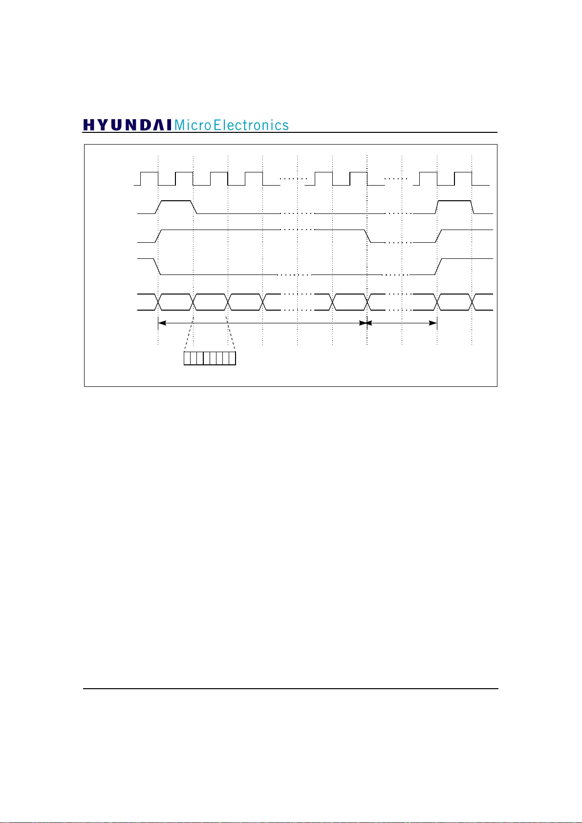
VSBCLK
VSBSOP
VSBDVALID
GDC21D003
NVSBERRFLG
VSBDATA[7:0]
47H byte0 byte1 byte186 0 47H0 byte0
1
with error
188 20
MSB of byte0 in the packet with error is set to ‘1’
Figure 6.6.8 I/F to Transport Demultiplexer when Register64[7:0] is set to Default Value
If only I2C register64[3](Derand_on) is set to ‘0’ and other values are reserved as the default,
1) the derandomizer is bypassed,
2) the data segment sync is set to 00H instead of 47H,
3) nothing is done at the MSB of the first data byte although the data segment has uncorrected errors.
See Fig. 6.6.9.
without error
68
Page 68
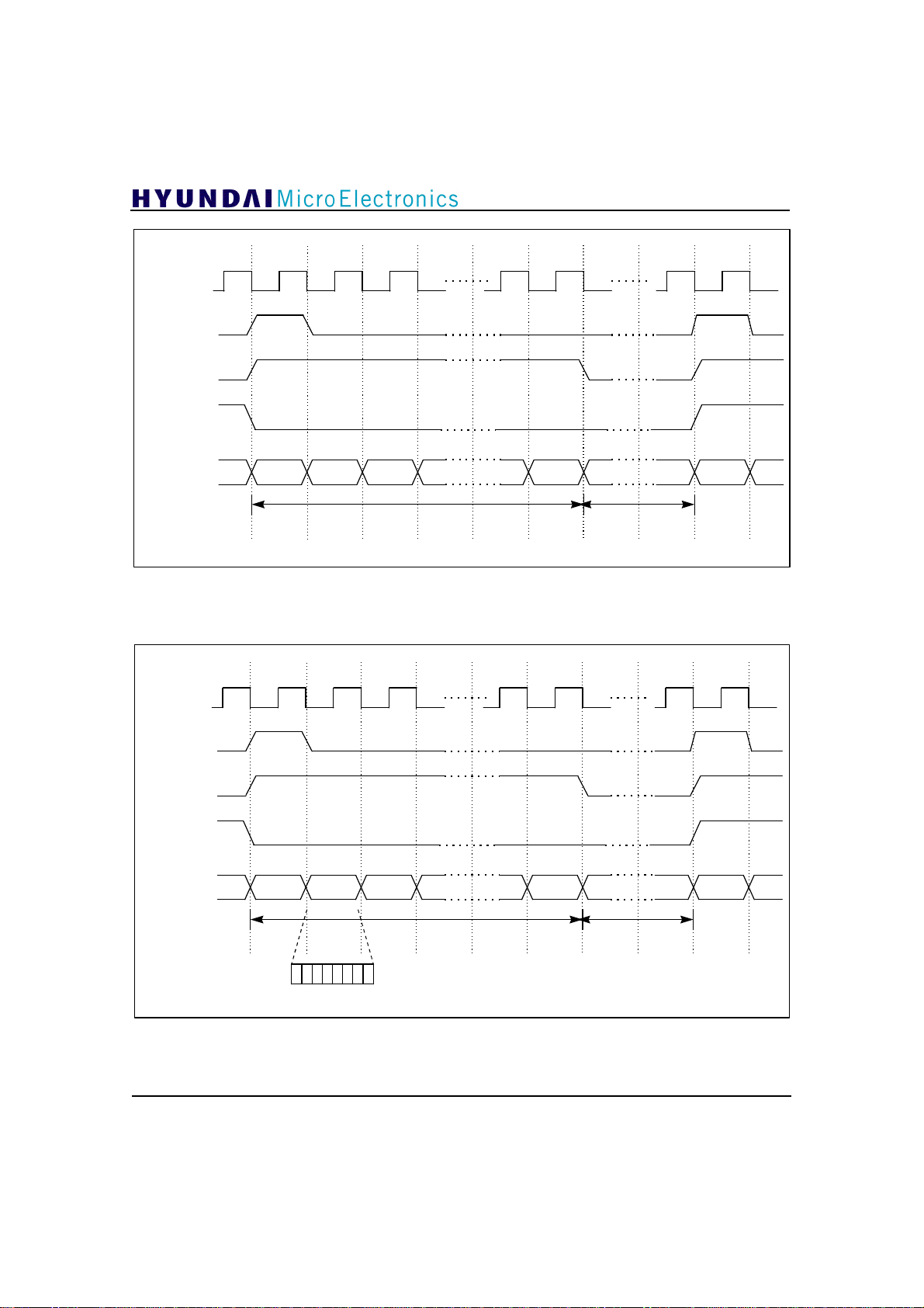
VSBCLK
VSBSOP
VSBDVALID
GDC21D003
NVSBERRFLG
VSBDATA[7:0]
00H byte0 byte1 byte186 parity values 00H byte0
with error
188 20
Figure 6.6.9 I/F to Transport Demultiplexer when Register64[3](Derand_on) is set to ‘ 0’
If only I2C register64[2](Errorflag_ins) is set to ‘0’ and other values are reserved as the default,
1) nothing is done at the MSB of the first data byte although the data segment has uncorrected errors. See Fig. 6.6.10.
VSBCLK
VSBSOP
VSBDVALID
NVSBERRFLG
with error
without error
without error
VSBDATA[7:0]
47H byte0 byte1 byte186 0 47H0 byte0
188 20
Nothing is done to the MSB of byte0 in the packet with error
(valid only when register64[3] is set to ‘1’)
Figure 6.6.10 I/F to Transport Demultiplexer when Register64[2](Errorflg_ins) is set to ‘ 0’
If only I2C register64[1](Vsbdvalid_pol) is set to ‘0’ and other values are reserved as the default,
1) signal VSBDVALID=’0’ and VSBDVALID=’ 1’ indicate valid data and invalid data interval respectively. See Fig. 6.6.11.
69
Page 69
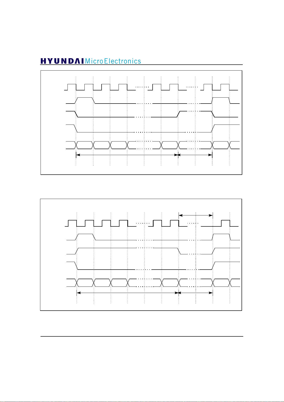
VSBCLK
VSBSOP
GDC21D003
VSBDVALID
NVSBERRFLG
VSBDATA[7:0]
polarity is inverted
with error
47H byte0 byte1 byte186 0 47H0 byte0
188 20
Figure 6.6.11 I/F to Transport Demultiplexer when Register64[1] is set to ‘ 0’
If only I2C register64[0](Vsbclk_sup) is set to ‘0’ and other values are reserved as the default,
1) the VSBCLK signal is suppressed to ‘0’ during VSBDVALID=’ 0’ interval. See Fig. 6.6.12.
suppressed to ‘0’
VSBCLK
VSBSOP
without error
VSBDVALID
NVSBERRFLG
VSBDATA[7:0]
47H byte0 byte1 byte186 0 47H0 byte0
with error
188 20
without error
Figure 6.6.12 I/F to Transport Demultiplexer when Register64[0](Vsbclk_sup) is set to ‘ 0’
At MMDS 8VSB mode, the duty cycle of VSBCLK is not 50% of VSBCLK period. Since 8 symbols compose 3
bytes, the duration of first byte equals to those of two symbols, and the duration of second and third byte is 3
symbols each. See Fig. 6.6.13.
70
Page 70
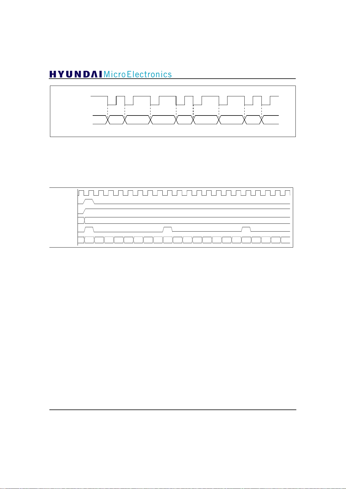
GDC21D003
H or L
VSBCLK
VSBDATA[7:0]
Figure 6.6.13 I/F to Transport Demultiplexer(MMDS 8VSB Mode)
If only I2C register64[7](pase) is set to ‘0’ and other values are reserved as the default, serial interface is offered.
1) the VSBDATA[7] signal indicates the start bit of a byte,
2) the VSBDATA[0] signal is the serial data output,
3) the VSBDATA[6:1] signals are set to “000000”. See Fig. 6.6.14.
VSBCLK
VSBSOP
VSBDVALID
NVSBERRFLG
VSBDATA[7]
VSBDATA[0]
b7 b6 b5 b4 b3 b2 b1 b0 b7 b6 b5 b40 1 0 0 0 1 1 1
......
Figure 6.6.14 I/F to Transport Demultiplexer at Serial Output Mode
Connection examples with VSB receivers and transport demultiplexer chips are shown in Fig. 6.6.15 - 6.6.17.
71
Page 71
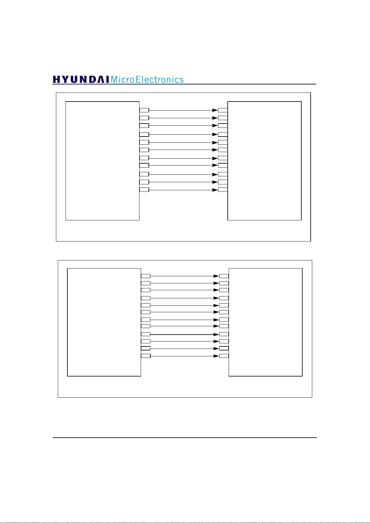
GDC21D003
7
6
A
6
VSBDATA[6]
VSBDATA[7]
VSBDATA[5]
VSBDATA[4]
VSBDATA[3]
VSBDATA[2]
VSBDATA[1]
VSBDATA[0]
VSBCLK
VSBDVALID
NVSBERRFLG
GDC21D003
VSB Receiver
80
77
75
74
72
71
69
68
89
84
83
30
FEC_DATA[7]
31
FEC_DATA[6]
36
FEC_DATA[5]
37
FEC_DATA[4]
38
FEC_DATA[3]
39
FEC_DATA[2]
40
FEC_DATA[1]
41
FEC_DATA[0]
32
FEC_CLOCK
43
\D_VALID
42
\ERR_BLOCK
GDC21D301
Transport Demultiplexer
Figure 6.6.15 Connection with VSB Receiver and Transport Demultiplexer Chip(GDC21D301A)
VSBDATA[6]
VSBDATA[7]
VSBDATA[5]
VSBDATA[4]
VSBDATA[3]
VSBDATA[2]
VSBDATA[1]
VSBDATA[0]
VSBCLK
VSBDVALID
NVSBERRFLG
VSBSOP
GDC21D003
CD[7]
CD[6]
CD[5]
CD[4]
CD[3]
CD[2]
CD[1]
CD[0]
CDCLK
CDEN
\CDERR
CDSYNC
L64007
(LSILOGIC)
VSB Receiver
Transport Demultiplexer
Figure 6.6.16 Connection with VSB Receiver and Transport Demultiplexer Chip(L64007)
72
Page 72
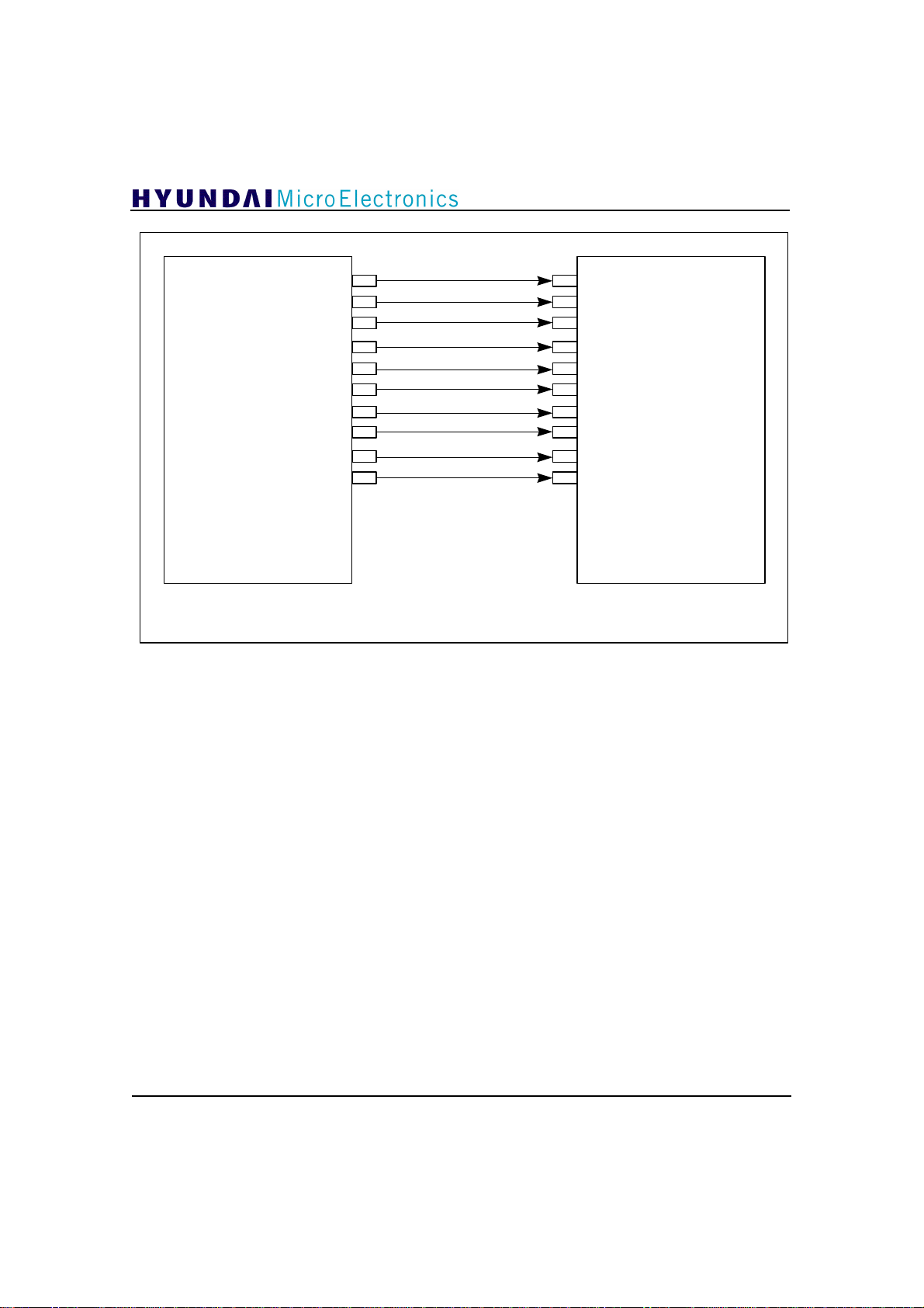
GDC21D003
7
VSBDATA[6]
VSBDATA[7]
VSBDATA[5]
VSBDATA[4]
VSBDATA[3]
VSBDATA[2]
VSBDATA[1]
VSBDATA[0]
VSBCLK
VSBDVALID
GDC21D003
VSB Receiver
Figure 6.6.17 Connection with VSB Receiver and Transport Demultiplexer Chip(AVIA-MAX)
6
CHDATA[7]
CHDATA[6]
CHDATA[5]
CHDATA[4]
CHDATA[3]
CHDATA[2]
CHDATA[1]
CHDATA[0]
CHCLK
CHEN
AVIA-MAX
(C-CUBE)
Transport Demultiplexer
73
Page 73
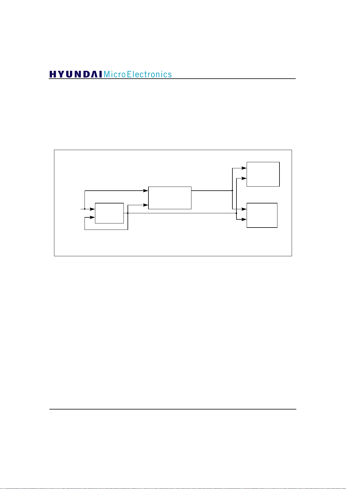
GDC21D003
6.7 PLL
The 4-times multiplexing scheme is used in the
256-tap filter. The PLL is used for generating the
4-times multiplying clock(CLK4EQ). Basically a
little jitter between SYMCLK and CLK4EQ may
occur. The clock skew due to the jitter can result in
abnormal operation in the paths related to both two
clocks. We used the following method to make
SYMCLK
4X-PLL
CLK4EQ
robust design against the clock skew. The
SYMCLK is delayed by 4 CLK4EQ-clock cycles.
The delayed clock is CLKEQ. Then the skew
between CLKEQ and CLK4EQ is fixed in spite of
the jitter of PLL. To fix skew is very useful
because it is difficult to estimate the accurate
amount of jitter. The scheme is shown in figure
6.7.1.
Equalizer
Control
CLKEQ
Clock Delay
Coefficient-
Update
Filter
74
Figure 6.7.1 Clock Scheme
Page 74
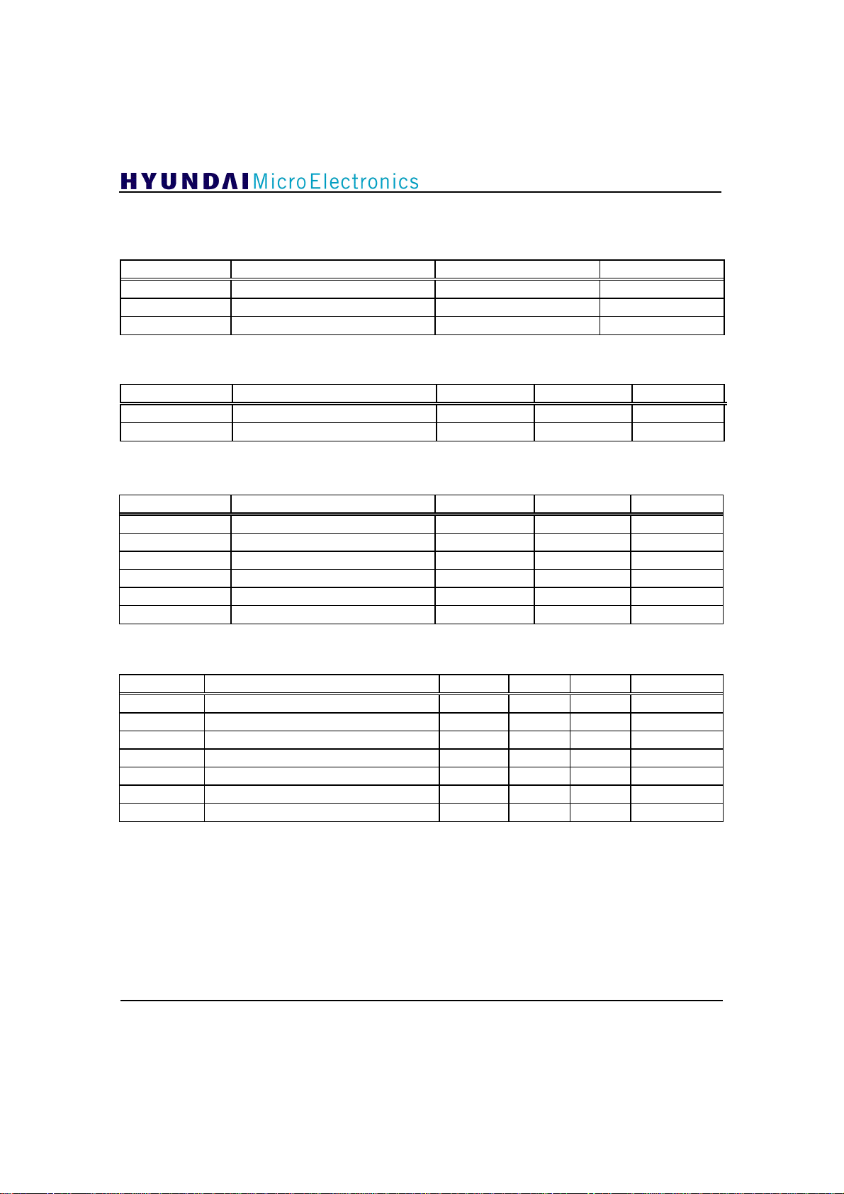
GDC21D003
7. Electrical Characteristics
Absolute Maximum Rating
SYMBOL PARAMETERS RATING UNIT
V
DD
V
I
T
stg
Recommended Operating Range
SYMBOL PARAMETERS MIN MAX UNIT
V
DD
T
opr
DC Characteristics (VDD = 3.15 V ~ 3.45 V, TA = 0 ~ 70 °C )
SYMBOL PARAMETERS MIN MAX UNIT
V
IH
V
IL
V
OH
V
OL
I
DD
I
DDS
AC Characteristics (VDD = 3.3 V ± 0.15, TA = 0 ~ 70 °C )
SYMBOL PARAMETERS MIN TYPE MAX UNIT
t
CP
t
IS
t
IH
* Output Delay time 29 ns
t
OD1
** Output Delay time 29 ns
t
OD2
t
CRH
t
IPL
Power Supply Voltage - 0.5 ~ 4.6 V
DC Input Voltage - 0.5 ~ V
+ 0.5 V
DD
Storage Temperature -25 ~ 150
Power Supply Voltage 3.15 3.45 V
Operating Temperature 0 70
Input High Voltage 0.7*VDD VDD + 0.5 V
Input Low Voltage - 0.5 0.3*VDD V
Output High Voltage 2.4 V
Output Low Voltage 0.4 V
Dynamic Supply Current 850 mA
Standby Current 30 mA
Clock SYMCLK Period 92.9 ns
Input Setup Time 10 ns
Input Hold Time 10 ns
Chip Reset Hold Time 20 t
Internal PLL Lock-up Time 1 ms
°C
°C
CP
* related pins are 68,69,71,72,74,75,77,80,83,84,85,89,108,110
** related pins are 43,44,46,52,53,55,56,57,66,90,92,93,95,96,97,100,102,103,104,106
75
Page 75
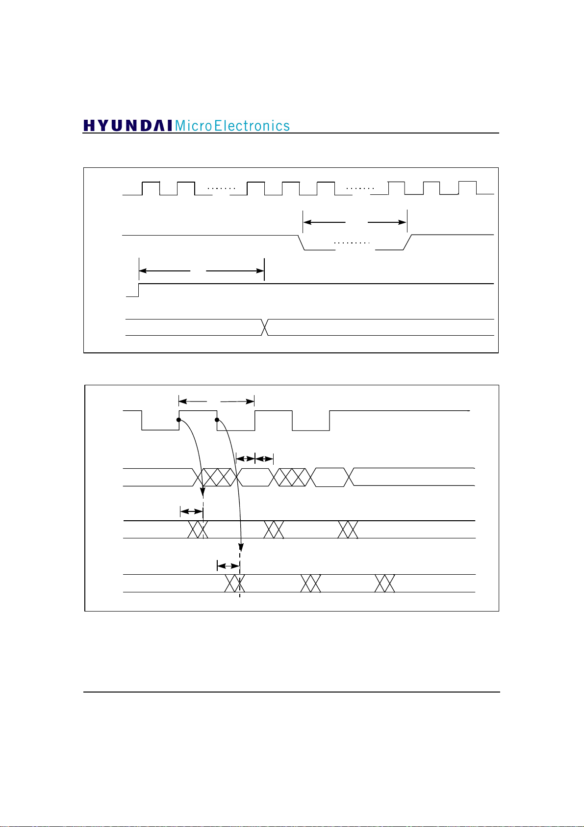
Timing Specification
SYMCLK
NRESET
POWER
GDC21D003
t
CRH
t
IPL
ALL IN/OUT
SYMCLK
Input
Output
Output
Not Valid
Figure 7.1 Clock Reset Stabilization Timing
t
CP
tISt
IH
t
OD1
t
OD2
Valid
76
Figure 7.2 Input and Output Timing
Page 76
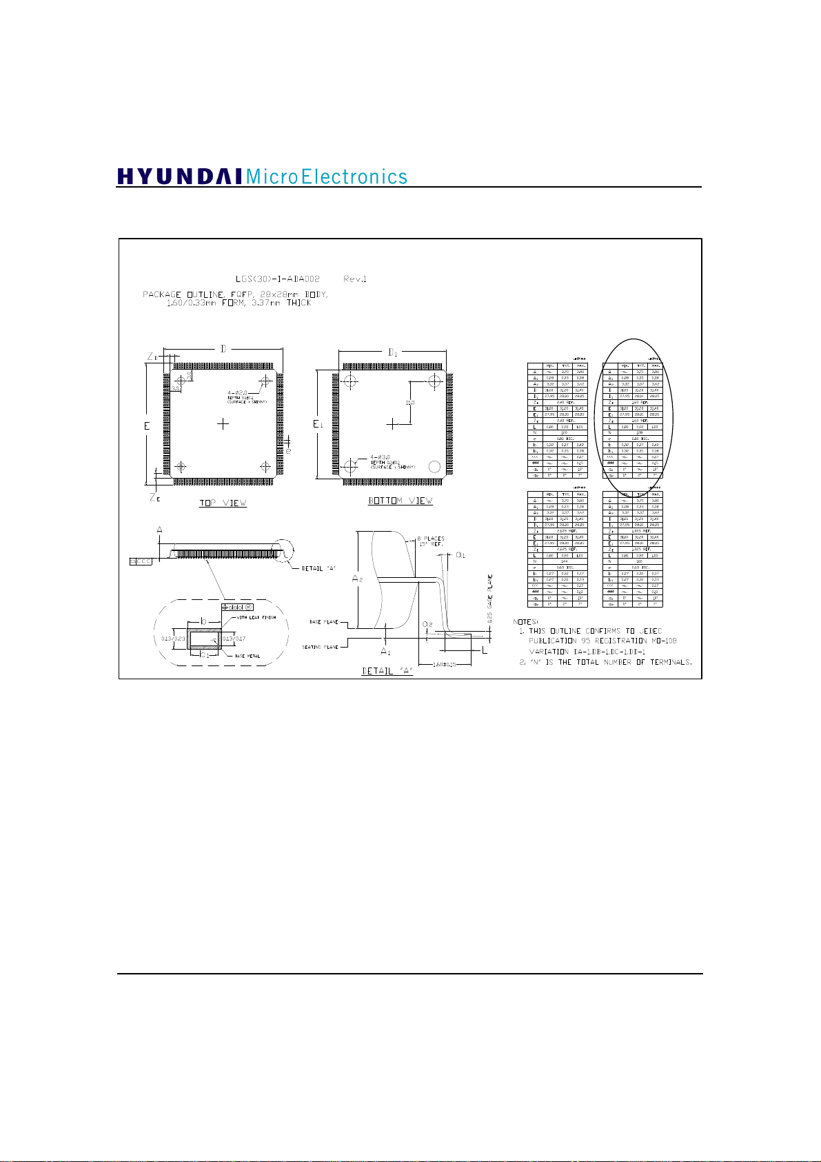
8. Package Dimensions
GDC21D003
Figure 8.1 Physical Dimensions
77
Page 77
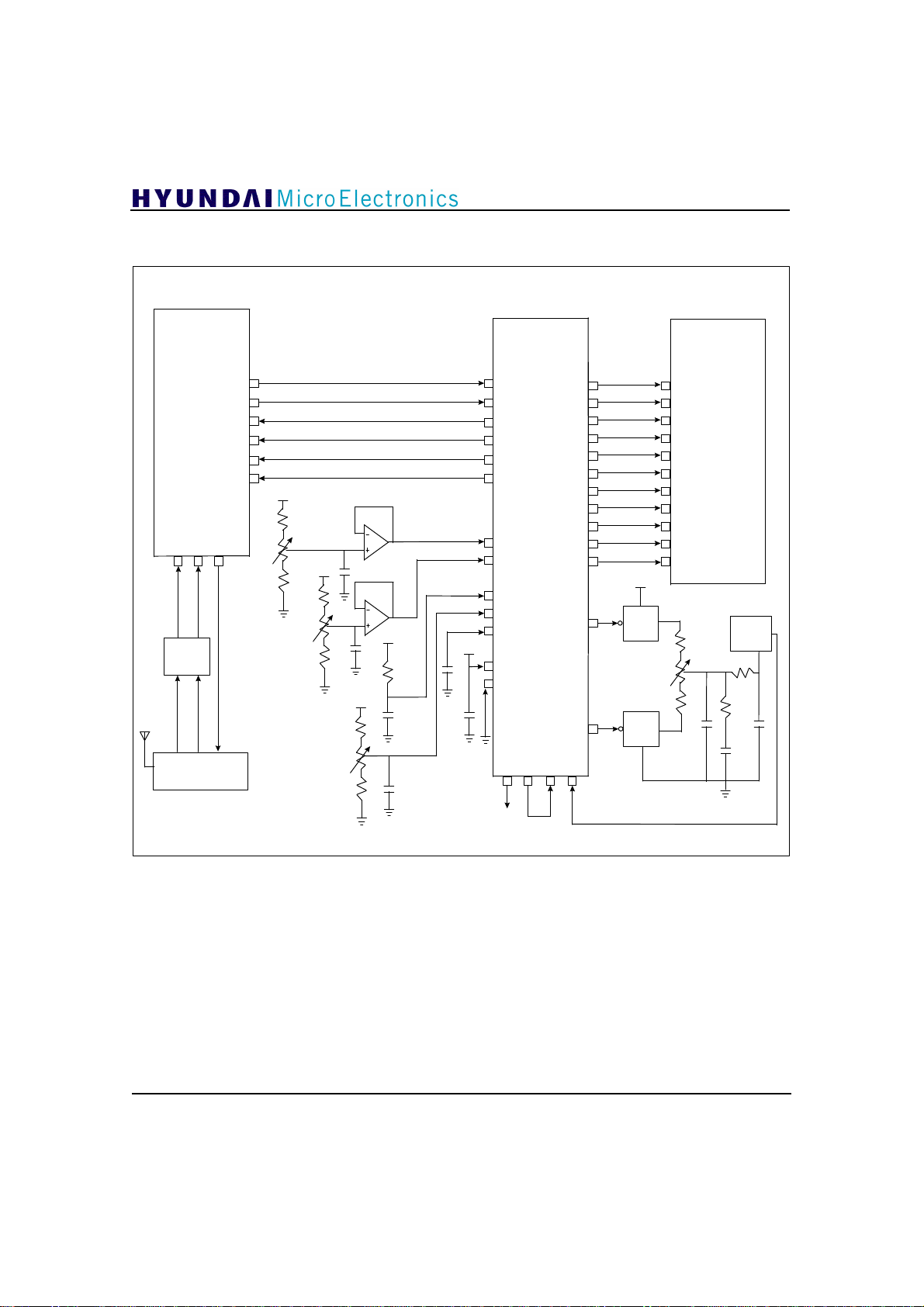
9. Application Notes
GDC21D003
Demodulation Chip
SANYO LA7785M
IOUT+
IOUT-
GUP
GDN
POLN
POLP
IFIN1
IFIN2
RFAGC
7
108
SAW
Filter
TUNER
VSB Receiver Chip
GDC21D003
30
29
21
20
22
23
3.3V
1.5K
2.2V
1.2V
3.3V
12K
0.1uF
1.5V
0.1uF
3.3K
1K
0.1uF
3.3V
3.3K
1K
2.0K
0.1uF
3.3V
3.3K
1K
2.7K
0.1uF
0.1uF
3.3V
125
INP
126
INN
52
GUP
53
GDN
43
DATAPOLN
44
DATAPOLP
124
REFP
123
REFN
2
REF
121
COM_0
128
BIAS
AVDD
AVSS
OPEN
ADCCLK
14 18
VSBDATA[7]
VSBDATA[6]
VSBDATA[5]
VSBDATA[4]
VSBDATA[3]
VSBDATA[2]
VSBDATA[1]
VSBDATA[0]
VSBCLK
VSBDVALID
NVSBERRFLG
NCHGUP
NCHGDN
SYMCLK
CLKFS
41 12
80
77
75
74
72
71
69
68
89
84
83
3.3V
56
Analog
S/W
57
Analog
S/W
VCXO
10.76MHz, 21.52MHz
10.76MHz, 21.52MHz, 43.04MHz & 75.32MHz
30
FEC_DATA[7]
31
FEC_DATA[6]
36
FEC_DATA[5]
37
FEC_DATA[4]
38
FEC_DATA[3]
39
FEC_DATA[2]
40
FEC_DATA[1]
41
FEC_DATA[0]
32
FEC_CLOCK
43
\D_VAILD
42
\ERR_BLOCK
6.8K
10K
6.8K
Transport Chip
GDC21D301
10K
3.6K
0.01uF
0.1uF
2.2uF
A
VCXO
78
Figure 9.1 VSB Receiver Application Circuit
 Loading...