

Page 1
GCU08AA-130
MITSUBISHI GATE COMMUTATED TURN-OFF THYRISTOR UNIT
GCU08AA-130
HIGH POWER INVERTER USE
PRESS PACK TYPE
● Symmetrical GCT
● GCT and Gate driver are connected
● I
TQRM
● I
T(AV) Average on-state current...................... 330A
● V
Repetitive controllable on-state current
DRM
Repetitive peak off-state voltage
............ 800A
.................. 6500V
APPLICATION
Inverters, DC choppers, Induction heaters, DC to DC converters.
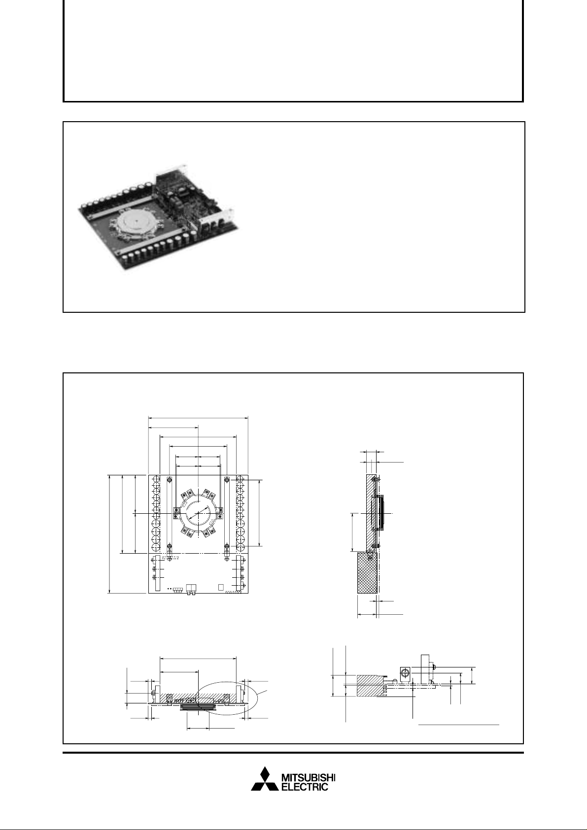
OUTLINE DRAWING Dimensions in mm
(208)
(104)
(160)
(250)
(165)
(80)(85)
(48) (46.5)
(46.5) (48)
G
K
G
K
TPG
TPX
LED4
LED3
LED2
LED1
(120)
K
φ47±0.2
G
K
DE2
DE1
G
K
G
K
G
(140)
(20)
9MAX
80±0.5
(5)
40MAX
160MIN
(80)
6±0.5 6±0.5
20MAX
6±0.5 6±0.5
φ47±0.2
10.1±0.9
26.2±0.3
A
14.5±1.3
10MIN
A PART MAGNIFICATION
(1.6)
(20)
(13.7)
Mar. 2001
Page 2
GCT PART (Type name : FGC800A-130DS)
MAXIMUM RATINGS
Symbol
V
RRM
VRSM
VDRM
VDSM
VLTDS
Repetitive peak reverse voltage
Non-repetitive peak reverse voltage
Repetitive peak off-state voltage
Non-repetitive peak off-state voltage
Long term DC stability voltage
Parameter
GK = –2V
V
GK = –2V
V
V
GK = –2V, λ = 100 Fit
MITSUBISHI GATE COMMUTATED TURN-OFF THYRISTOR UNIT
GCU08AA-130
HIGH POWER INVERTER USE
PRESS PACK TYPE
Conditions
—
—
Voltage class
6500
6500
6500
6500
3600
Unit
V
V
V
V
V
Symbol Parameter Conditions
V
ITQRM
T(RMS)
I
IT(AV)
ITSM
2
I
t
diT/dt
VFGM
VRGM
IFGM
IRGM
PFGM
PRGM
PFG(AV)
PRG(AV)
Tj
Tstg
—
—
Repetitive controllable on-state current
RMS on-state current
Average on-state current
Surge on-state current
Current-squared, time integration
Critical rate of rise of on-state current
Peak forward gate voltage
Peak reverse gate voltage
Peak forward gate current
Peak reverse gate current
Peak forward gate power dissipation
Peak reverse gate power dissipation
Average forward gate power dissipation
Average reverse gate power dissipation
Junction temperature
Storage temperature
Mounting force required
Weight
DM = 3/4 VDRM, VD = 3000V, LC = 0.3µH, VRG = 20V
T
j = 25/115°C, With GU-D08 (see Fig. 1, 3)
Applied for all conduction angles
f = 60Hz, sinewave θ = 180°, T
One half cycle at 60Hz, T
V
D = 3000V, IT = 800A, CS= 0.1µF, RS= 10Ω
j = 25/115°C, f = 60Hz, With GU-D08 (see Fig. 1,2 )
T
j = 115°C Start
(Recommended value 13kN)
Typical value
ELECTRICAL CHARACTERISTICS
Symbol Parameter Conditions
TM
V
IRRM
IDRM
IGRM
d
v/dt
tgt
td
Eon
ts
E
off
QRR
Erec
IGT
VGT
Rth(j-f)
On-state voltage
Repetitive peak reverse current
Repetitive peak off-state current
Reverse gate current
Critical rate of rise of off-state voltage
Turn-on time
Delay time
Turn-on switching energy
Storage time
Turn-off switching energy
Reverse recovery charge
Reverse recovery energy
Gate trigger current
Gate trigger voltage
Thermal resistance
T = 800A, Tj = 1 15°C
I
V
RM = 6500V, Tj = 115°C
V
DM = 6500V, VGK = –2V, Tj = 115°C
RG = 21V, Tj = 115°C
V
V
D = 3000V, VGK = –2V, Tj = 115°C
(Expo. wave) (see Fig. 4)
I
T = 800A, VD = 3000V, di/dt = 1000A/µs, Tj = 115°C
C
S= 0.1µF, RS = 10Ω
With GU-D08 (see Fig. 1, 2)
T = 800A, VDM = 3/4 VDRM, VD = 3000V
I
C
S= 0.1µF, RS= 10Ω, VRG = 20V, Tj = 115°C
With GU-D08 (see Fig. 1, 5)
V
R = 3000V, I T = 800A, di/dt = 1000A/µs
C
S= 0.1µF, RS = 10Ω, Tj = 115°C (see Fig. 5, 6)
DC METHOD : VD = 24V, RL = 0.1Ω, Tj = 25°C
Junction to fin
f = 55°C
Ratings
800
520
330
4.8
4
9.6 × 10
1000
10
21
500
800
5
17
100
120
–20 ~ +115
–20 ~ +150
11.1 ~ 15.8
530
Limits
Min Typ Max
—
—
—
—
3000
—
—
—
—
—
—
—
—
—
—
—
—
—
150
100
—
—
—
—
—
—
—
—
1650
—
—
—
—
0.025
6.8
50
—
5.0
1.0
1.6
3.0
6.0
5.0
0.5
1.5
Unit
A
A
A
kA
2
A
A/µs
V
V
A
A
kW
kW
W
W
°C
°C
kN
g
Unit
V
mA
mA
mA
V/µs
µs
µs
J/P
µs
J/P
µ
C
J/P
A
V
°C/W
s
Mar. 2001
Page 3
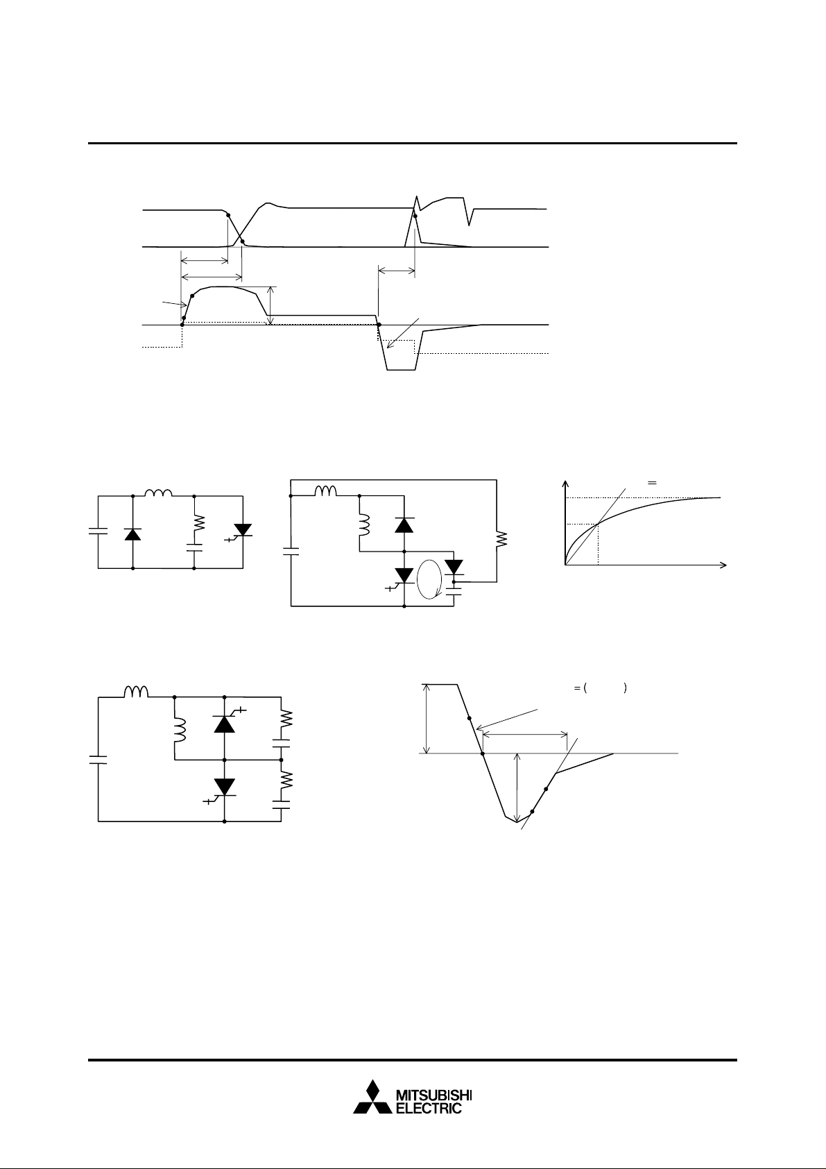
Fig. 1 Turn-on and Turn-off waveform
τ
V
D
dV/dt0.632VD/τ
0.632V
D
t
V
D
t
d
t
gt
diG/d
t
V
RG
I
GM
MITSUBISHI GATE COMMUTATED TURN-OFF THYRISTOR UNIT
GCU08AA-130
HIGH POWER INVERTER USE
PRESS PACK TYPE
I
T
t
s
I
G
di
I
GQ/dt
GQ
V
D
td ; 0VG ~ 0.9V
t
gt
; 0VG ~ 0.1V
diG/dt ; 0.1IGM ~ 0.9I
ts ; 0VG ~ 0.9I
diGQ/dt ; 0.1IGQ ~ 0.9I
V
RG
D
D
GM
T
GQ
Fig. 2 Turn-on test circuit Fig. 3 Turn-off test circuit
Fig. 4 dv/dt test waveform
(With clamp circuit)
L
Rs
V
D
Cs
GCT
V
D
L(line)
L(load)
GCT
FWDi
Lc
CDi
Cc
Rc
Fig. 5 Turn-off and Recovery test circuit Fig. 6 Reverse recovery waveform
V
D
L (line)
L (load)
GCT1
GCT2
Rs
Cs
Rs
Cs
QRR t
i/dt
50%I
T
I
T
d
t
rr
0
I
RM
90%I
rr × IRM
(0 ~ 50%IT)
50%I
RM
RM
GCT1 : For turn-off test
GCT2 : For Recovery test
/2
Mar. 2001
Page 4

GATE DRIVER PART (Type name : GU-D08)
Symbol
VC
P Power consumption (Note 2)
f
fd
t
trd
diG/dt
IGM
tW
IG
diGQ/dt
Dmax
Ta
Power supply (Note 1)
—
Control signal (Note 3)
Frequency
Delay time of on gate current
Delay time of off gate current
Critical rate of rise of on gate current
Peak on gate current
Width of on high gate current
On gate current
Critical rate of rise of off gate current
Maximum duty
Temperature
Status signal (Note 4)
—
Parameter Conditions
DC power supply
T = 330A, f = 780Hz
I
Optical fiber data link
Transmitter : HFBR-1521 (HP)
Receiver : HFBR-2521 (HP)
T = 330A, Duty 33%
I
T
j ≥ –10°C
RG= 20V
V
Operation temperature (Recommend : ≤ 40°C)
MITSUBISHI GATE COMMUTATED TURN-OFF THYRISTOR UNIT
GCU08AA-130
HIGH POWER INVERTER USE
PRESS PACK TYPE
Limits
Min Typ Max
19
—
2.5
—
—
—
—
—
50
—
3
1.25
—
—
–10
—
20
—
—
—
—
—
—
—
90
—
—
1200
—
—
—
780
100
+60
21
—
35
—
3.0
3.0
—
—
—
—
—
—
Unit
V
W
—
Hz
µs
µs
A/µs
A
µs
A
A/µs
%
°C
—
Fig. 7 Gate current, gate voltage and control signal waveform
G/dt
di
(10A ~ 80A)
GATE CURRENT
GATE VOLTAGE
t
fd
G
V
t
w
= 0
80A
I
GM
I
G
di
GQ
VG = 0
/dt
t
rd
I
GQ
V
RG
50%
CONTROL SIGNAL
Note 1. (1) Guaranteed power supply voltage for operation is 19V minimum and 21V maximum.
(2) When over voltage occurs, GDU voltage bus (G-K voltage for GCT) is clamped to be 21V if mamimum voltage for input gata voltage from power
supply is 25V and maximum duration of over voltage higher than 21V from power supply is 0.4 sec when control signal is on (Please see Fig. 8).
(3) When over voltage occurs, GDU voltage bus is clamped to be 21V with no time limitation if maximum voltage from power supply is 25V and control
signal is off (Please see Fig. 8).
Note 2. GCT is off state and no gate signal is supplied for gate driver. No leakage current flows between gate and cathode of GCT.
Note 3. Optic fiber data link HFBR-1521 and HFBR-2521 are interlocked each other.
on
t
T = 1/f
off
t
Mar. 2001
Page 5

Note 4.
1. Status signal from LED
(1) Status signal
Status of GCT
On state
Off state
LED 1
(Red)
OFF
ON
(2) Fault signal
Status
Normal
Fault
Fault
Fault
G-K PS
Normal
Normal
G-K short
G-K short
MITSUBISHI GATE COMMUTATED TURN-OFF THYRISTOR UNIT
LED 2
(Yellow)
ON
OFF
20±1V
Voltage down
20±1V
Voltage down
PS LED
(LED 4)
On
Off, V < 17.5V (Typ.)
On
Off, V < 17.5V (Typ.)
GCU08AA-130
HIGH POWER INVERTER USE
PRESS PACK TYPE
G-K LED
(LED 3)
On
Off (If V > 12.5V (Typ.) then LED 3 is on)
Off
Off
2. Status signal from Transmitter (Note 5) (L : Light NL : No light)
(1) Normal operation
Control signal
(Control board)
Control signal
(GDU input)
Status signal
(GDU output)
(3) Fault signal (G-K short)
Control signal
(Control board)
Control signal
(GDU input)
Status signal
(GDU output)
Normal Fault
L
NL
L
NL
L
NL
L
NL
L
NL
L
NL
(2) Fault signal (O/V or U/V)
Control signal
(Control board)
Control signal
(GDU input)
Status signal
(GDU output)
(3) Fault signal (fiber optic)
Control signal
(Control board)
Control signal
(GDU input)
Status signal
(GDU output)
Normal
NL
NL
L
NL
L
NL
L
L
L
NL
Fault
(Always No light)
L
(Always light)
Note 5. About over voltage fault signal, please see Fig. 8.
Mar. 2001
Page 6

Fig. 8 Over voltage fault signal timing chart
Power supply voltage
25V
Maximum Guaranteed Voltage (Note 6)
22V
21V
19V
t
1
GDU Voltage bus (G-K Voltage for GCT)
21V
MITSUBISHI GATE COMMUTATED TURN-OFF THYRISTOR UNIT
GCU08AA-130
HIGH POWER INVERTER USE
PRESS PACK TYPE
t
3
t
2
(Note 8)
19V
Status Signal
Control Signal
Fault signal start System shut down
1t1 < 1.0ms (Max. repetition rate ; 1 pulse/100ms)
2
t
2 ≥ 1.0ms
3
t
3 < 0.4sec
Note 6. Maximum peak voltage of GDU input voltage from power supply should be lower than 25V.
Note 7. If the period for over voltage < 1.0ms (period t1), no fault signal is sent.
` If the period for over voltage ≥ 1.0ms, fault signal starts after period t2 from 22V of power supply voltage. System should be shut down (Control signal
should be off) within period t3 from fault signal start.
Note 8. GDU Voltage bus (G-K Voltage for GCT) is clamped to be 21V if power supply voltage is higher than 21V after system shut down (control signal off).
Control signal off
Mar. 2001
Page 7

PERFORMANCE CURVES
MAXIMUM ON-STATE CHARACTERISTIC
4
10
7
5
)
3
A
(
2
3
10
7
5
3
2
Tj=115°C
2
10
7
5
ON-STATE CURRENT
3
2
10
012345678
ON-STATE VOLTAGE (V
Tj=25°C
MITSUBISHI GATE COMMUTATED TURN-OFF THYRISTOR UNIT
GCU08AA-130
HIGH POWER INVERTER USE
PRESS PACK TYPE
on
VS I
T
E
2.5
Condition
(J/P)
on
TURN ON SWITCHING ENERGY E
)
D
=3000V, Tj=115°C
V
di/dt=1000A/µs
2.0
Cs=0.1µF, Rs=10Ω
With GU-D08
1.5
1.0
0.5
0.0
TURN ON CURRENT IT (A)
Max
Typ
10000
900800700600500400300200100
E
off
VS I
T
9
(J/P)
Condition
off
8
V
D
=3000V, VDM=VD+2.34∗I
Tj=115°C, With GU-D08
7
Cs=0.1µF, Rs=10Ω
T
6
5
4
3
2
1
0
TURN OFF SWITCHING ENERGY E
0
100 200 300 400 500 600 700 800 9001000
Turn-off and
Recovery test circuit
L(load)
V
D
GCT1:Turn-off test
GCT2:Recovery test
TURN OFF CURRENT IT (A)
Q
RR
VS I
T
2500
(µC)
Condition
RR
V
R
=3000V, Tj=115°C
di/dt=1000A/µs
2000
Cs=0.1µF, Rs=10Ω
1500
1000
500
0
REVERSE RECOVERY CHARGE Q
0 100 200 300 400 500 600 700 800 9001000
Turn-off and
Recovery test circuit
L(load)
V
D
GCT1:Turn-off test
GCT2:Recovery test
ON-STATE CURRENT IT (A)
E
rec
VS I
T
8
(J/P)
rec
Max
Typ
L(line)
Rs
Cs
GCT2
Rs
GCT1
Cs
REVERSE RECOVERY ENERGY E
Condition
7
R
=3000V, Tj=115°C
V
di/dt=1000A/µs
6
Cs=0.1µF, Rs=10Ω
5
4
3
2
1
0
0
100 200 300 400 500 600 700 800 9001000
Turn-off and
Recovery test circuit
L(line)
L(load)
V
D
GCT1
GCT1:Turn-off test
GCT2:Recovery test
Max
Typ
GCT2
Rs
Cs
Rs
Cs
ON-STATE CURRENT IT (A)
MAXIMUM THERMAL IMPEDANCE
CHARACTERISTIC
(JUNCTION TO FIN)
0.035
0.03
Max
0.025
0.02
Typ
L(line)
Rs
Cs
GCT2
Rs
GCT1
Cs
0.015
0.01
0.005
THERMAL IMPEDANCE Zth(°C/W)
0
0.001 0.01 0.1 1 10
TIME (S)
Mar. 2001
 Loading...