

Page 1
ULTRAFAST MSM PHOTODETECTORS
p
G4176 SERIES (GaAs)
PRELIMINARY DATA
Ultrafast response of several tens picosecond
FEATURES
Ultrafast response
G4176 : tr , tf = 30 ps (Typ.)
G7096 : t
Low dark current
G4176 : 100 pA (Ta=25
Large photosensitive area
200 µm
APPLICATIONS
Optical high-speed waveform measurements
Optical communications
= 40 ps (Typ.)
r
°C)
G7096 SERIES (InGaAs)
G4176
G7096
G4176-01
G7096-01
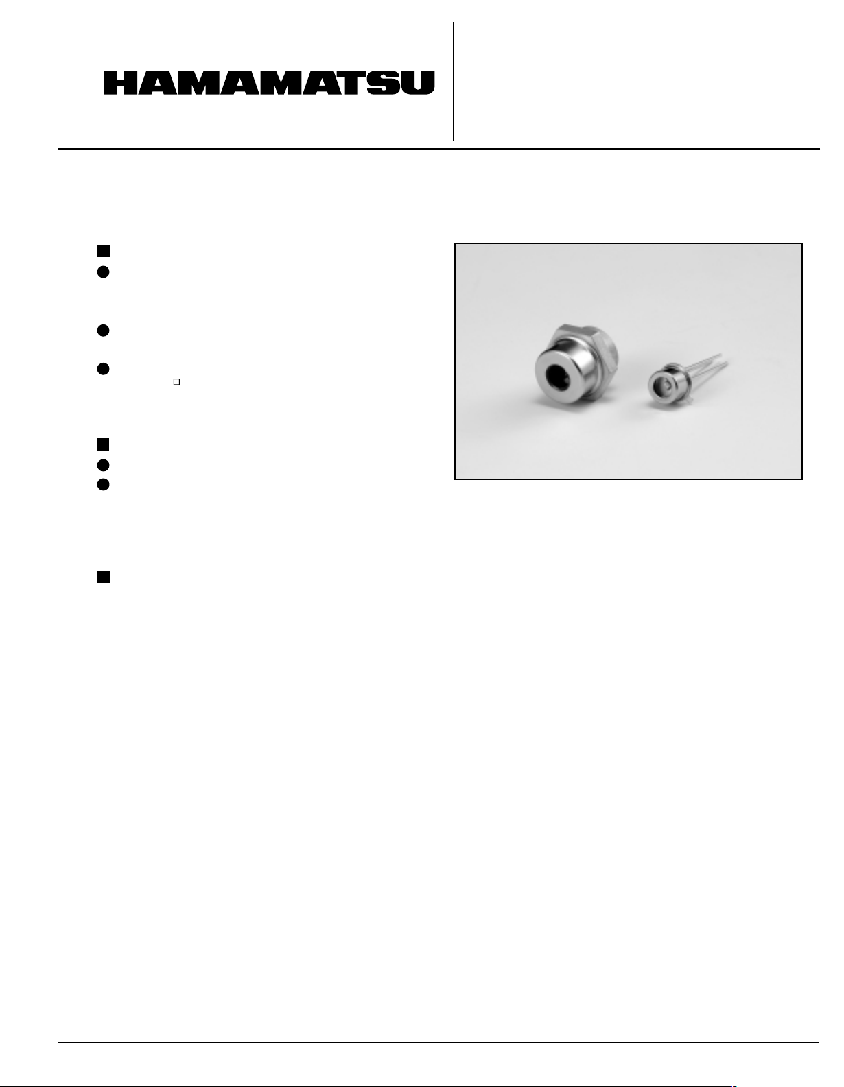
DESCRIPTION
HAMAMATSU realized MSM (Metal-Semiconductor-Metal) Photodetectors having ultrafast responses.
The GaAs MSM Photodetector G4176 features 30ps response time for both rise & fall while keeping a low dark
current (100pA at Ta=25 °C). The rise time of the InGaAs MSM Photodetector G7096 is 40ps.
Symmetrical and interdigital Schottky contacts are fabricated at the sensitive area, whose size can be larger than
other kinds of fast response photodetectors. This makes easier to set up with optics. Therefore, MSM
Photodetectors are suited for measurements of optical high-speed waveform and optical communications.
There is no electrical polarity in MSM Photodetectors, that is, both polarities of a bias voltage are available, and
the polarity of an output signal depends on its connection.
Two kinds of packages are prepared for each MSM Photodetector. The package of G4176 & G7096 is a coaxial
metal type (patent : Japan 2070802), which is easy to connect with an electrical SMA-connector. That of G417601 & G7096-01 is a TO-18, which is very common.
An optical fiber or connector input types are available as a custom option. Contact your local representative for
more information.
Information furnished by HAMAMATSU is believed to be reliable. However, no responsibility is assumed for possible inaccuracies or omissions.
ecifications are subject to change without notice. No patent rights are granted to any of the circuits described herein. '2003 Hamamatsu Photonics K.K.
S
Page 2
ULTRAFAST MSM PHOTODETECTORS G4176 SERIES (GaAs)
,
G4176 SERIES
G7096 SERIES (InGaAs)
ABSOLUTE MAXIMUM RATINGS (Ta=25°C)
Item
Maximum Bias Voltage
Maximum Light Input
Pulsed Light
CW to Pulsed Light
Operating Temperature
Storage Temperature
Symbol
V
b
Φ
T
op(a)
T
stg
Condition
Pulse width
Pulse width
1ns
1ns
Value
10
50
5
-40 to +85
-40 to +100
GENERAL CHARACTERISTICS (Ta=25°C)
Item
Spectral Response Range
Peak Response Wavelength
Effective Sensitive Area
Symbol
λ
λ
p
A
Condition
V
= 7 V
b
V
= 7 V
b
Chip Size
Package
G4176
G4176-01
Figure 1: Optical Pulse Response
G4176
(Including time response of light source, bias-tee and oscilloscope)
1.1
1.0
0.9
0.8
0.7
0.6
0.5
0.4
Output (arb. unit)
0.3
0.2
0.1
0
Value
450 to 870
850
0.2 0.2
1 1
TO-5
(Unified with SMA connector)
TO-18
(Vb = 7 V)
Unit
V
mW
mW
°C
°C
Unit
nm
nm
mm
mm
ELECTRICAL AND OPTICAL CHARACTERISTICS (Ta=25°C, Vb=7V)
Radiant sensitivity
Dark Current
*
NEP
G4176
G4176-01
Terminal Capacitance
G4176
G4176-01
Rise Time
G4176
2
G4176-01
2
Fall Time
G4176
G4176-01
*Noise Equivalent Power
**Value on Chip
G4176-01
(Including time response of light source, assembly circuit and oscilloscope)
Output (arb. unit)
Item
1.1
1.0
0.9
0.8
0.7
0.6
0.5
0.4
0.3
0.2
0.1
0
Symbol
**
S
I
d
C
t
t
r
t
f
Condition
λ = 850 nm
λ = 850 nm
10 to 90 %
90 to 10 %
0.2 X 10
0.2 X 10
Min.
0.2
-
-
-
-
-
-
-
-15
-15
Value
Typ.
0.3
100
3 X 10
4 X 10
0.3
0.5
30
50
30
50
-15
-15
Max.
-
300
-
-
0.4
0.6
40
80
40
80
Unit
A/W
pA
W/Hz
pF
ps
ps
1/2
(Vb = 7 V)
Time (0.1ns/
Figure 2: Spectral Response
0
10
-1
10
-2
10
Radiant Sensitivity (A/W)
-3
10
500300 900700600400 1000800
div
)
(Vb = 7 V)
Time (0.1ns/
div
)
Page 3

G7096 SERIES
ABSOLUTE MAXIMUM RATINGS (Ta=25°C)
Item
Maximum Bias Voltage
Maximum Light Input
Pulsed Light
CW to Pulsed Light
Operating Temperature
Storage Temperature
Symbol
V
b
Φ
T
op(a)
T
stg
Condition
Pulse width
Pulse width
1ns
1ns
Value
15
10
2
-40 to +85
-40 to +100
GENERAL CHARACTERISTICS (Ta=25°C)
Item
Spectral Response Range
Peak Response Wavelength
Effective Sensitive Area
Chip Size
Package
G7096
G7096-01
Figure 3: Optical Pulse Response
G7096
(Including time response of light source, bias-tee and oscilloscope)
1.1
1.0
0.9
0.8
0.7
0.6
0.5
0.4
Output (arb. unit)
0.3
0.2
0.1
0
Symbol
λ
λ
p
A
Condition
V
= 10 V
b
= 10 V
V
b
Value
850 to 1650
1500
0.2 0.2
1 1
TO-5
(Unified with SMA connector)
TO-18
(Vb = 10 V)
Unit
V
mW
mW
°C
°C
Unit
nm
nm
mm
mm
ELECTRICAL AND OPTICAL CHARACTERISTICS (Ta=25°C, Vb=10V)
Radiant sensitivity
Dark Current
*
NEP
G7096
G7096-01
Terminal Capacitance
G7096
G7096-01
Rise Time
G7096
2
G7096-01
2
Fall Time
G7096
G7096-01
*Noise Equivalent Power
**Value on Chip
G7096-01
(Including time response of light source, assembly circuit and oscilloscope)
Output (arb. unit)
Item
1.1
1.0
0.9
0.8
0.7
0.6
0.5
0.4
0.3
0.2
0.1
0
Symbol
**
S
I
d
C
t
t
t
r
f
Condition
λ = 1.3 µm
µm
λ = 1.3
10 to 90 %
90 to 10 %
0.2 X 10
0.2 X 10
Min.
0.2
-
-
-
-
-
-
-
-10
-10
Value
Typ.
0.4
5
2 X 10
3 X 10
0.7
0.9
40
80
120
160
-10
-10
Max.
-
20
-
-
0.8
1.0
60
100
160
200
Unit
A/W
µA
W/Hz
pF
ps
ps
1/2
(Vb = 10 V)
Time (0.1ns/
Figure 4: Spectral Response
0
10
-1
10
-2
10
Radiant Sensitivity (A/W)
-3
10
0.6
0.8
1.0
1.2
div
)
1.4
(Vb = 10 V)
1.6
1.8
Time (0.1ns/
div
)
Page 4

ULTRAFAST MSM PHOTODETECTORS G4176 SERIES (GaAs)
,
CONNECTION EXAMPLES
G7096 SERIES (InGaAs)
G4176
G7096
Optical Input
BIAS-TEE
G4176
(G7096)
BIAS
CASE
Power Supply
+ (or -)
- (or +)
DIMENSIONAL OUTLINES (Unit : mm)
G4176
G7096
Electric Output
Optical Input
G4176-01
(G7096-01)
G4176-01
G7096-01
G4176-01
G7096-01
100 Ω
BIAS
10 kΩ
Output
Case Lead
Electric Output
Coaxial Connector
10 nF
Power Supply
- (or +)
+ (or -)
CHIP
SENSITIVE
SURFACE
2.3
1/4-36UNS-2B
10
φ8.2
φ7.9
(BOTTOM VIEW)
9.6
2.03.0
CASE
OUTPUT/BIAS
*
Both polarities of the bias voltage are available.
*
CHIP
SENSITIVE
SURFACE
φ0.45LEAD
φ5.4
φ4.7
(BOTTOM VIEW)
1.2
12 min. 3.6
BIAS / OUTPUT
OUTPUT / BIAS
CASE
*
*
http://www.hamamatsu.com
HAMAMATSU PHOTONICS K.K., Laser Group, Sales Dept.
5000, Hirakuchi, Hamakita City, Shizuoka, 434-8601, Japan, Telephone: (81)53-584-0227, Fax: (81)53-584-0228, E-mail: laser-g@lsr.hpk.co.jp
U.S.A.: Hamamatsu Corporation:360 Foothill Road, P.O. BOX 6910, Bridgewater, N.J. 08807-0910, U.S.A.Telephone: (1)908-231-0960, Fax: (1)908-231-1218 E-mail: usa@hamamatsu.com
Germany: Hamamatsu Photonics Deutschland GmbH: Arzbergerstr. 10, D-82211 Herrsching am Ammersee, Germany, Telephone: (49)8152-375-0, Fax: (49)8152-2658, E-mail: info@hamamatsu.de
France: Hamamatsu Photonics France S.A.R.L.: 8, Rue du Saule Trapu, Parc du Moulin de Massy, 91882 Massy Cedex, France, Telephone: 33(1) 69 53 71 00, Fax: 33(1) 69 53 71 10, E-mail: infos@hamamatsu.fr
United Kingdom: Hamamatsu Photonics UK Limited: 2 Howard Court, 10 Tewin Road, Welwyn Garden City, Hertfordshire AL7 1BW, United Kingdom, Telephone: (44)1707-294888, Fax: (44)1707-325777, E-mail: info@hamamatsu.co.uk
North Europe: Hamamatsu Photonics Norden AB: Smidesv gen 12, SE-171-41 Solna, Sweden, Telephone: (46)8-509-031-00, Fax: (46)8-509-031-01, E-mail: info@hamamatsu.se
-
-
-
f
Cat. No. LPRD1022E01
 Loading...