

Page 1
CML Semiconductor Products
Analogue Control Interface
FX839
1.0 Features
• Three DACs
8 or 10-Bit Resolution
• Custom IRQ Generator with Variable
8-Bit Reference Settings
• Multiplexed 4 Input ADC
10-Bit Resolution
• Scalable ADC Clock Frequencies
from Xtal/Clock
• Two Variable Attenuators • Serial Interface to Host µC
• Low Power (3.0V Operation) • 24-Pin SSOP Package
September 1997
D/839/4
Advance Information
1.1 Brief Description
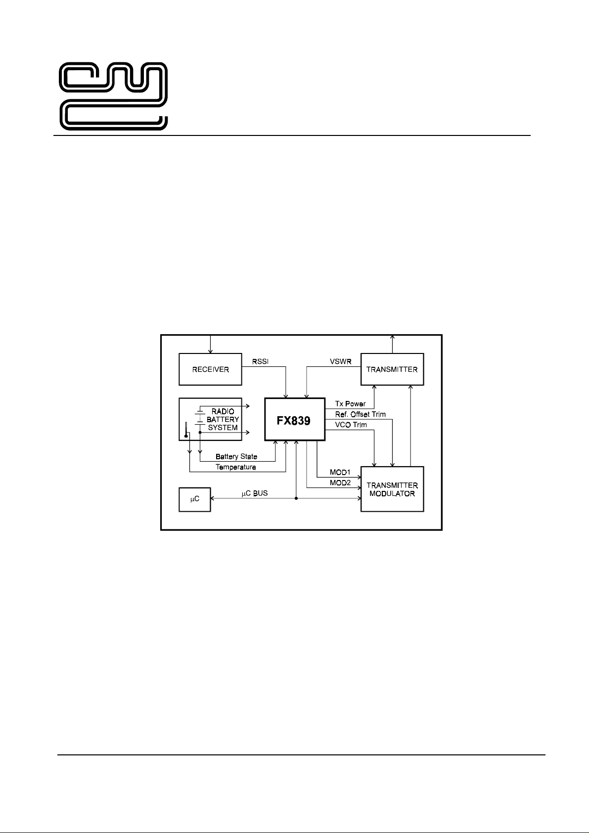
This product comprises a selection of independent functional blocks vital to modern microcomputer controlled
radio-frequency communications equipment. Examples of possible uses are as follows:
The four-way multiplexed ADC with magnitude comparator may be used for monitoring RSSI, battery
•
voltage, temperatures, reflected signals or error voltages.
The three DACs may be used to adjust VCOs, reference oscillators, power output, bias current or IF gain.
•
The two variable attenuators may be used to adjust deviation, modulation depth or baseband gain.
•
The FX839 is controlled via the standard serial 'C-BUS'. This is complementary to, and c ompatible with, many
standard microcomputers and other baseband processing blocks.
Consumer Microcircuits Limited
1997
Page 2

Analogue Control Interface
Section
1.0 Features..........................................................................................................1
1.1 Brief Description............................................................................................1
1.2 Block Diagram................................................................................................3
1.3 Signal List.......................................................................................................4
1.4 External Components.................................................................................... 6
1.5 General Description....................................................................................... 7
1.5.1 Software Description
1.6 Application Notes.........................................................................................15
1.6.1 General
1.7 Performance Specification.......................................................................... 16
1.7.1 Electrical Performance
1.7.2 Packaging
FX839
CONTENTS
Page
.....................................................................8
..........................................................................................15
................................................................16
.....................................................................................21
Note:
As this product is still in development, it is likely that a number of changes and additions will be made to
this specification. Items marked TBD or left blank will be included in later issues. Information in this
data sheet should not be relied upon for final product design.
Consumer Microcircuits Limited 2
1997
D/839/4
Page 3
Analogue Control Interface
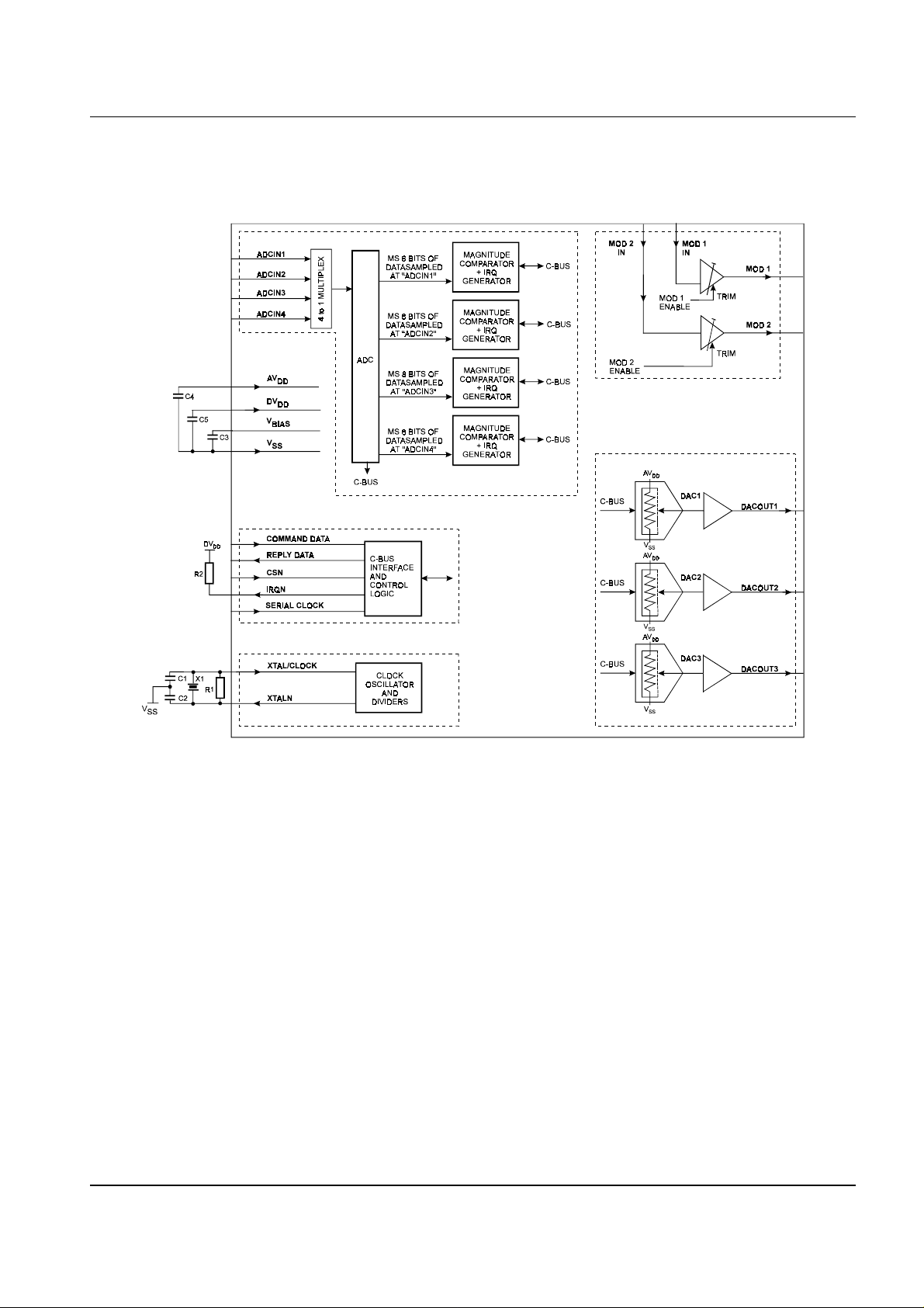
1.2 Block Diagram
FX839
Consumer Microcircuits Limited 3
1997
Figure 1: Block Diagram
D/839/4
Page 4

Analogue Control Interface
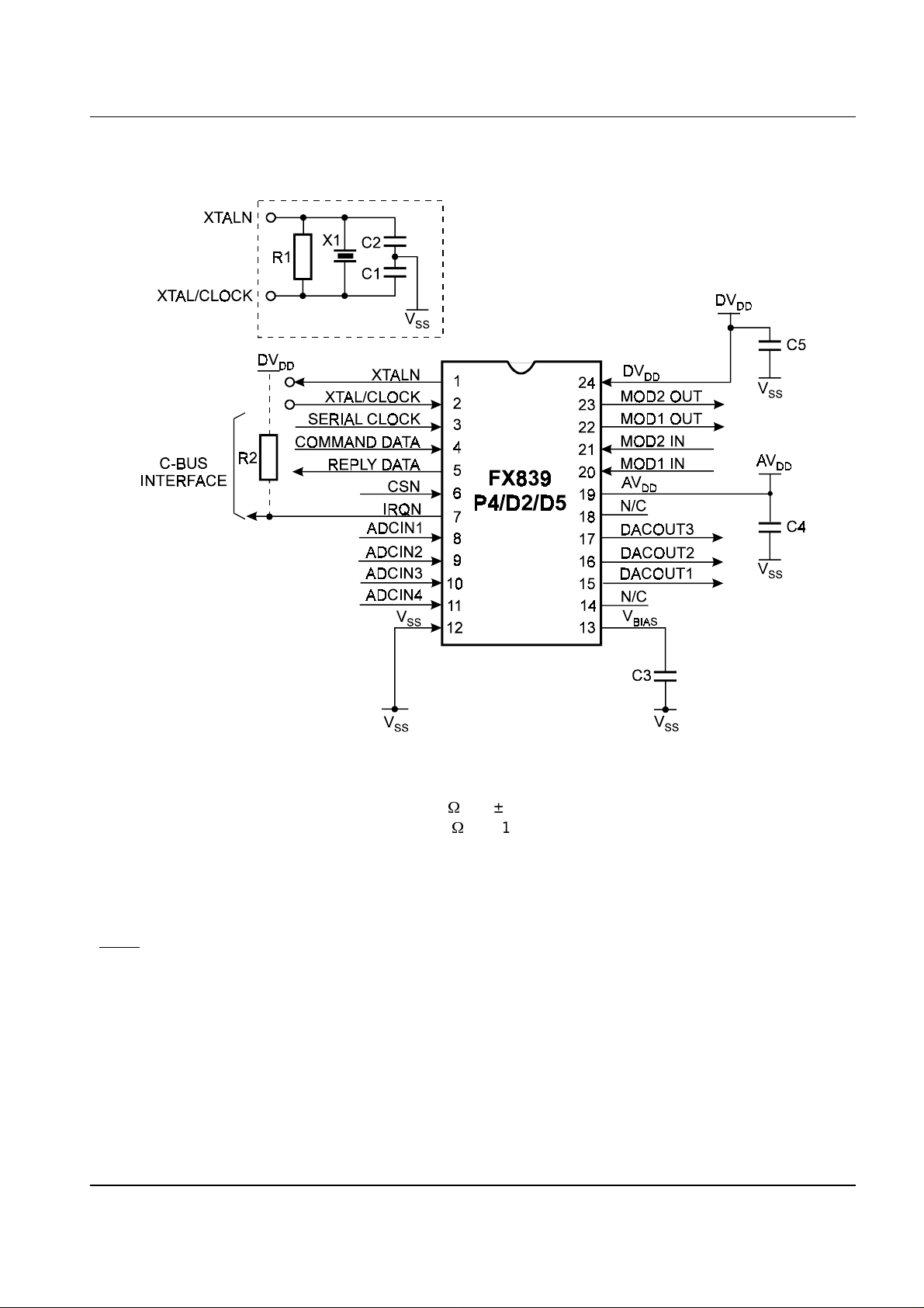
1.3 Signal List
FX839
Package
P4/D2/D5
Signal Description
Pin No. Name Type
1 XTALN O/P The inverter output of the on-chip oscillator.
2 XTAL/CLOCK I/P The input to the on-chip oscillator, for external Xtal circuit
or clock.
3 SERIAL
CLOCK
I/P The 'C-BUS' serial clock input. This clock, produced by
the µController, is used for transfer timing of commands
and data to and from the device.
See 'C-BUS' Timing Diagram (Figure 4).
4 COMMAND
DATA
I/P The 'C-BUS' serial data input from the µController. Data is
loaded into this device in 8-bit bytes, MSB (B7) first, and
LSB (B0) last, synchronised to the SERIAL CLOCK.
See 'C-BUS' Timing Diagram (Figure 4).
5 REPLY DATA O/P The 'C-BUS' serial data output to the µController. The
transmission of REPLY DATA bytes is synchronised to the
SERIAL CLOCK under the control of the CSN input.
This 3-state output is held at high impedance when not
sending data to the µController. See 'C-BUS' Timing
Diagram (Figure 4).
6 CSN I/P The 'C-BUS' data loading control function: this input is
provided by the µController. Data transfer sequences are
initiated, completed or aborted by the CSN signal.
See 'C-BUS' Timing Diagram (Figure 4).
7 IRQN O/P This output indicates an interrupt condition to the
µController by going to a logic '0'. This is a 'wire-ORable'
output, enabling the connection of up to 8 peripherals to 1
interrupt port on the µController. This pin has a low
impedance pulldown to logic '0' when active and a highimpedance when inactive. An external pullup resistor is
required.
The conditions that cause interrupts are indicated in the
IRQ FLAG register and are effective if not disabled.
8 ADCIN1 I/P Analogue to digital converter input 1 (ADC1)
9 ADCIN2 I/P Analogue to digital converter input 2 (ADC2)
Consumer Microcircuits Limited 4
1997
D/839/4
Page 5

Analogue Control Interface
FX839
1.3 Signal List
Package
P4/D2/D5
(continued)
Signal Description
Pin No. Name Type
10 ADCIN3 I/P Analogue to digital converter input 3 (ADC3)
11 ADCIN4 I/P Analogue to digital converter input 4 (ADC4)
12 V
SS
P
OWER
The negative supply rail (ground) for both analogue and
digital supplies.
13 V
BIAS
O/P An analogue bias line for the internal circuitry, held at ½
. This pin must be decoupled by a capacitor mounted
AV
DD
close to the device pins.
14 N/C No internal connection. Do not make any connection to
this pin.
15 DACOUT1 O/P Digital to analogue converter No. 1 output (DAC1)
16 DACOUT2 O/P Digital to analogue converter No. 2 output (DAC2)
17 DACOUT3 O/P Digital to analogue converter No. 3 output (DAC3)
18 N/C No internal connection. Do not make any connection to
this pin.
19 AV
DD
P
OWER
The positive analogue supply rail. Analogue levels and
voltages are dependent upon this supply. This pin should
be decoupled to V
by a capacitor.
SS
20 MOD1 IN I/P Input to MOD1 variable attenuator.
21 MOD2 IN I/P Input to MOD2 variable attenuator.
22 MOD1 O/P Output of MOD1 variable attenuator.
23 MOD2 O/P Output of MOD2 variable attenuator.
24 DV
DD
P
OWER
The positive digital supply rail. Digital levels and voltages
are dependent upon this supply. This pin should be
by a capacitor.
SS
Notes:
decoupled to V
I/P = Input
O/P = Output
Consumer Microcircuits Limited 5
1997
D/839/4
Page 6
Analogue Control Interface
1.4 External Components
FX839
C1 22pF ±20% R1 1M
C2 22pF ±20% R2 22k
C3 0.1µF ±20%
C4 0.1µF ±20%
C5 0.1µF ±20%
Notes
: 1. If an external clock is to be used, it should be connected to Pin 2 and the components C1, C2,
R1 and X1 omitted. The ADC clock frequency is derived from the cryst al or external clock by
means of internal programmable dividers. Refer to Section 1.7 for details of cry stal or external
clock frequency range.
Figure 2: Recommended External Components
Consumer Microcircuits Limited 6
1997
±5% X1 Note 1
:
±10%
:
D/839/4
Page 7

Analogue Control Interface
FX839
1.5 General Description
The device comprises four groups of r elated functions: variable attenuators, digital to analogue converters, a
multiplexed analogue to digital converter with multiplexer, clock generator and four 8-bit magnitude
comparators with variable reference lev els. These functions are all controlled by the 'C-BUS' serial interface
and are described below:
Variable Attenuators
The two variable attenuators have a range of 0 to -12dB and 0 to -6dB respectively and may be c ontrolled
independently.
Digital to Analogue Converters
Three DACs are provided with default resolutions of 8 bits, which are defined at the initial chip reset. In this
mode the 'C-BUS' data is transferred in a single byte. An option is provided to define any one or more of the
DAC resolutions to be 10 bits, then the DAC requires the transfer of two 'C-BUS' data bytes.
The upper and lower DAC reference voltages are defined internally as AV
and VSS respectively. The output
DD
voltage is expressed as:
= AVDD x (DATA / 2n) [Volts]
V
OUT
Where, n is the DAC resolution (8 or 10 bits) and DATA is the dec imal v alue of the input code. For ex ample: n
= 8 and binary code = 11111111 therefore DATA = 255
= AVDD x (255 / 256) [Volts]
V
OUT
Any one of the three DAC input latches may be loaded by sending an address/command byte followed by one
or two data bytes to the 'C-BUS' interface. The data is then latc hed and the static voltage is updated at the
appropriate output.
When a DAC is disabled its output is defined as open-circuit.
Analogue to Digital Converter and ADC Clock Generator
A single successive approximation ADC is provided with four multiplexed inputs. In order to minimise the
sampling time of each input channel, a Sample and Hold circuit has not been included at the input of the ADC.
For the sampling to be accurate the input signal should not change significantly during the conver sion time.
Since the typical application is for the monitoring of slowly changing control voltages this should not present
any problems. The maximum signal 'linear rate of change', 'S', can be quantified by the following expres sion
(for a maximum 1 bit error):
Where f
S = AV
is the internal ADC clock frequency.
adc_clk
DD
x f
/ (210 x 1000 x (10 + 2)) [mV/µs]
adc_clk
The programmable clock generator is intended to be flexible, making use of an external system clock signal or
a dedicated crystal. This clock signal is scaled to provide the internal ADC cloc k frequency ( f
adc_clk
). The user
has full control of the frequency scaling fac tor and this s hould be chos en s uc h that the input cloc k frequenc y , at
the XTAL/CLOCK pin, divided by this factor is no more than 1MHz.
Consumer Microcircuits Limited 7
1997
D/839/4
Page 8

Analogue Control Interface
FX839
The microcontroller is required to wait during the c onver s ion time, T
conv_max
(Figure 3), before issuing a 'READ
ADC DATAx' command. If this is not done, then the converted data returned on 'C-BUS' will be the result of the
previous conversion on the selected channel. It is possible for the data conversion rate to exceed the reply rate
on 'C-BUS'. In such a case, the data returned will be the result of the most recent conversion completed.
Figure 3: Example of a "conversion and read"
*T
conv_max
is directly related to the ADC clock frequency, which in turn is set by the ex ternal clock frequency
and the clock divider.
T
conv_max
= ((10 + 2) x '
NUMBER OF ENABLED MUX INPUTS'
/ f
adc_clk
)
[Seconds
]
Note that after reading the ADC1 data, it is necessary to re- enable the c onver s ion of data by setting Bit 5 of the
ADC Control Register to ‘1’.
Magnitude Comparators and Interrupt Request
High and low digital comparator reference levels are provided for the four digital magnitude comparators via the
'C-BUS' interface. The digital input to the comparators is provided by the most significant 8 bits of each ADC
data.
When the sampled data falls outside the high or low digital comparator referenc e levels the status register is
updated and the IRQN pin is pulled low. When a reference level is set to '0', its IRQ is disabled.
1.5.1 Software Description
Address/Commands
Instructions and Data are transferred via the 'C-BUS' in accordance with the timing information given in
Figure 4.
Instruction and data transactions to and from the FX839 consis t of an Addr ess /Command by te followed
by either:
(i) a control or DAC data write (1 or 2 bytes) or,
(ii) a status or ADC data read (1 or 2 bytes)
Consumer Microcircuits Limited 8
1997
D/839/4
Page 9

Analogue Control Interface
Write Only Register (8-Bit and 16-Bit)
HEX
ADDRESS/
COMMAND
$01 RESET N/A N/A N/A N/A N/A N/A N/A N/A
$D0 CONTROL 0 0000BIT 2 BIT 1 BIT 0
$D2 ATTENUATOR (1) 0 0 ENABLE BIT 4 BIT 3 BIT 2 BIT 1 BIT 0
$D3 CONTROL DAC1 DAC2 DAC3 0 ENABLE ENABLE ENABLE 0
$D4 (1) BIT 7 BIT 6 BIT 5 BIT 4 BIT 3 BIT 2 BIT 1 BIT 0
$D5 (1) BIT 7 BIT 6 BIT 5 BIT 4 BIT 3 BIT 2 BIT 1 BIT 0
$D6 (1) BIT 7 BIT 6 BIT 5 BIT 4 BIT 3 BIT 2 BIT 1 BIT 0
$D7 CONTROL 0 1 READN ACTIVE ACTIVE ACTIVE ACTIVE 0
$D8 LEVELS (1) BIT 7 BIT 6 BIT 5 BIT 4 BIT 3 BIT 2 BIT 1 BIT 0
$D9 LEVELS (1) BIT 7 BIT 6 BIT 5 BIT 4 BIT 3 BIT 2 BIT 1 BIT 0
$DA LEVELS (1) BIT 7 BIT 6 BIT 5 BIT 4 BIT 3 BIT 2 BIT 1 BIT 0
$DB LEVELS (1) BIT 7 BIT 6 BIT 5 BIT 4 BIT 3 BIT 2 BIT 1 BIT 0
REGISTER
NAME
CLOCK/IRQ DIVIDER
VARIABLE MOD1 MOD1
VARIABLE MOD2 MOD2
ATTENUATOR (2) 0 0 ENABLE BIT 4 BIT 3 BIT 2 BIT 1 BIT 0
DAC NBIT NBIT NBIT DAC1 DAC2 DAC3
DAC1 DATA
BIT 7
(D7)
BIT 6
(D6)
BIT 5
(D5)
BIT 4
(D4)
BIT 3
(D3)
BIT 2
(D2)
BIT 1
(D1)
*See Note 1
(2) 000000BIT 9 BIT 8
DAC2 DATA
*See Note 1
(2) 000000BIT 9 BIT 8
DAC3 DATA
*See Note 1
(2) 000000BIT 9 BIT 8
ADC ADCIN1 ADCIN2 ADCIN3 ADCIN4
MAG COMP ONE MAGNITUDE COMPARATOR UPPER LEVEL
MAG COMP ONE MAGNITUDE COMPARATOR LOWER LEVEL
LEVELS (2) BIT 7 BIT 6 BIT 5 BIT 4 BIT 3 BIT 2 BIT 1 BIT 0
MAG COMP TWO MAGNITUDE COMPARATOR UPPER LEVEL
MAG COMP TWO MAGNITUDE COMPARATOR LOWER LEVEL
LEVELS (2) BIT 7 BIT 6 BIT 5 BIT 4 BIT 3 BIT 2 BIT 1 BIT 0
MAG COMP THREE MAGNITUDE COMPARATOR UPPER LEVEL
MAG COMP THREE MAGNITUDE COMPARATOR LOWER LEVEL
LEVELS (2) BIT 7 BIT 6 BIT 5 BIT 4 BIT 3 BIT 2 BIT 1 BIT 0
MAG COMP FOUR MAGNITUDE COMPARATOR UPPER LEVEL
MAG COMP FOUR MAGNITUDE COMPARATOR LOWER LEVEL
LEVELS (2) BIT 7 BIT 6 BIT 5 BIT 4 BIT 3 BIT 2 BIT 1 BIT 0
FX839
BIT 0
(D0)
Note 1:
A second byte is expected by the 'C-BUS' interface only when the 'NBIT DAC
Control Register' is set high. Otherwise the data transfer is a single byte (Bit 7 to Bit 0).
Consumer Microcircuits Limited 9
1997
n
' bit of the 'DAC
D/839/4
Page 10

Analogue Control Interface
Read Only Registers (8-Bit and 16-Bit)
HEX
ADDRESS/
COMMAND
$D1
$DC
$DD
$DE
$DF
REGISTER
NAME
IRQ
FLAGS HIRQF4 LIRQF4 HIRQF3 LIRQF3 HIRQF2 LIRQF2 HIRQF1 LIRQF1
ADC DATA1
(1) BIT 7 BIT 6 BIT 5 BIT 4 BIT 3 BIT 2 BIT 1 BIT 0
(2) 000000BIT 9 BIT 8
ADC DATA2
(1) BIT 7 BIT 6 BIT 5 BIT 4 BIT 3 BIT 2 BIT 1 BIT 0
(2) 000000BIT 9 BIT 8
ADC DATA3
(1) BIT 7 BIT 6 BIT 5 BIT 4 BIT 3 BIT 2 BIT 1 BIT 0
(2) 000000BIT 9 BIT 8
ADC DATA4
(1) BIT 7 BIT 6 BIT 5 BIT 4 BIT 3 BIT 2 BIT 1 BIT 0
(2) 000000BIT 9 BIT 8
BIT 7
(D7)
BIT 6
(D6)
BIT 5
(D5)
BIT 4
(D4)
BIT 3
(D3)
BIT 2
(D2)
BIT 1
(D1)
FX839
BIT 0
(D0)
Write Only Register Description
RESET Register (Hex Address $01)
The reset command has no data attached to it. It sets the device registers into the specific states listed below:
REGISTER NAME BIT 7
(D7)
CLOCK/IRQ CONTROL 00000000
DAC CONTROL 00000000
DAC1 DATA
DAC2 DATA
DAC3 DATA
ADC CONTROL 00000000
VARIABLE ATTENUATOR (1) 00000000
MAG COMP ONE LEVELS (1) 00000000
MAG COMP TWO LEVELS (1) 00000000
MAG COMP THREE LEVELS (1) 00000000
MAG COMP FOUR LEVELS (1) 00000000
Note 1:
1
1
1
(2)00000000
(2)00000000
(2)00000000
(2)00000000
(2)00000000
Default resolution is defined as 8-Bits.
BIT 6
(D6)
00000000
00000000
00000000
BIT 5
(D5)
BIT 4
(D4)
BIT 3
(D3)
BIT 2
(D2)
BIT 1
(D1)
BIT 0
(D0)
Consumer Microcircuits Limited 10
1997
D/839/4
Page 11

Analogue Control Interface
CLOCK/IRQ CONTROL Register (Hex Address $D0)
This register controls the ADC clock divide ratio:
FX839
Bits 7 to 3
DIVIDER
(Bit 2 to Bit 0)
Reserved for future use. These bits should be set to '0'.
The input clock divide ratio, which sets the ADC cloc k fr equenc y is defined in the
following table:
Bit 2 Bit 1 Bit 0 Function
0 0 0 Powersave
001
010
011
100
101
110
111
1
÷
2
÷
4
÷
8
÷
16
÷
32
÷
64
÷
Consumer Microcircuits Limited 11
1997
D/839/4
Page 12

Analogue Control Interface
FX839
VARIABLE ATTENUATOR Register (Hex address $D2)
This is a 16-bit register. Byte (1) is sent first. Bits 0 - 5 of the first byte in this register are used to enable and
set the attenuation of the Modulator 1 amplifier and bits 0 - 5 of the second byte in this r egister are used to
enable and set the attenuation of the Modulator 2 amplifier, according to the tables below:
BYTE 1 BYTE 2
543210 Mod. 1 Attenuation 543210 Mod. 2 Attenuation
0XXXXX Disabled (V
100000 >40dB 100000 >40dB
100001 12.0dB 100001 6.0dB
100010 11.6dB 100010 5.8dB
100011 11.2dB 100011 5.6dB
100100 10.8dB 100100 5.4dB
100101 10.4dB 100101 5.2dB
100110 10.0dB 100110 5.0dB
100111 9.6dB 100111 4.8dB
101000 9.2dB 101000 4.6dB
101001 8.8dB 101001 4.4dB
101010 8.4dB 101010 4.2dB
101011 8.0dB 101011 4.0dB
101100 7.6dB 101100 3.8dB
101101 7.2dB 101101 3.6dB
101110 6.8dB 101110 3.4dB
101111 6.4dB 101111 3.2dB
110000 6.0dB 110000 3.0dB
110001 5.6dB 110001 2.8dB
110010 5.2dB 110010 2.6dB
110011 4.8dB 110011 2.4dB
110100 4.4dB 110100 2.2dB
110101 4.0dB 110101 2.0dB
110110 3.6dB 110110 1.8dB
110111 3.2dB 110111 1.6dB
111000 2.8dB 111000 1.4dB
111001 2.4dB 111001 1.2dB
111010 2.0dB 111010 1.0dB
111011 1.6dB 111011 0.8dB
111100 1.2dB 111100 0.6dB
111101 0.8dB 111101 0.4dB
111110 0.4dB 111110 0.2dB
111111 0dB 111111 0dB
) 0XXXXX Disabled (V
BIAS
BIAS
)
X = don't care
MOD1 ENABLE
(Bit 5, first byte)
MOD2 ENABLE
(Bit 5, second byte)
(Bits 7 and 6, first
When this bit is '1' the MOD1 attenuator is enabled.
When this bit is '0' the MOD1 attenuator is disabled (i.e. powersaved).
When this bit is '1' the MOD2 attenuator is enabled.
When this bit is '0' the MOD2 attenuator is disabled (i.e. powersaved).
Reserved for future use. These should be set to '0'.
and second bytes)
Consumer Microcircuits Limited 12
1997
D/839/4
Page 13

Analogue Control Interface
DAC CONTROL Register (Hex address $D3)
This register controls the resolution and the number of enabled DAC outputs:
NBIT DAC1, NBIT DAC2, NBIT DAC3
(Bit 7 to Bit 5)
These bits define the input resolutions for each of the four DACs. When 'NBIT
DAC
' is '0' the resolution of DACn is 8-Bits. When 'NBIT DACn is '1' the
n
resolution of DAC
is 10-Bits.
n
FX839
Bit 4
Reserved for future use. This bit should be set to '0'.
DAC1 ENABLE, DAC2 ENABLE, DAC3 ENABLE
(Bit 3 to Bit 1)
These bits allow any one or more of the three DACs to be powered up. When '0'
the DAC
is powered down and the output is high impedance. When '1' the DAC
n
is powered on and the output voltage is defined by the DAC Data Registers.
Bit 0
Reserved for future use. This bit should be set to '0'.
DAC1 DATA Register (Hex Address $D4)
DAC2 DATA Register (Hex Address $D5)
DAC3 DATA Register (Hex Address $D6)
The data in these three registers sets the analogue v oltage at the output of DAC1, DAC2 and DAC3. This data
will consist of one or two bytes depending on the defined input resolution which is s et by bits 7, 6 and 5 of the
DAC Control Register. When operating with 10-bit resolution Bit 7 to Bit 2 of the DAC
DATA Register second
n
data byte must be set to "0".
ADC CONTROL Register (Hex Address $D7)
This register controls the resolution, active inputs and conversion modes of the ADC as described below:
Bit 7
Reserved for future use. This bit should be set to '0'.
Bit 6
Reserved for future use. This bit should be set to ‘1’.
(On reset, this bit is set to ‘0’).
READN
(Bit 5)
When this bit is set to '1' all active input channels are c ontinuously sampled and
the latest converted data stored for each channel. When this bit is set to ‘0’ all
conversions are stopped so that they may be read.
ADC1 ACTIVE, ADC2 ACTIVE, ADC3 ACTIVE, ADC4 ACTIVE
(Bit 4 to Bit 1)
These bits allow any one or more of the four ADC input channels to be enabled.
When '0' the ADCIN
input voltage is not converted. When '1' the ADCINn input
n
is defined as active and the input voltage is converted.
Note: ADC1 must always be enabled for any other channel to work.
(Bit 0)
Consumer Microcircuits Limited 13
1997
Reserved for future use. This bit should be set to ‘0’.
D/839/4
Page 14

Analogue Control Interface
FX839
MAG COMP ONE LEVELS (Hex Address $D8)
MAG COMP TWO LEVELS (Hex Address $D9)
MAG COMP THREE LEVELS (Hex Address $DA)
MAG COMP FOUR LEVELS (Hex Address $DB)
Each address controls the relevant numbered ADC magnitude comparator.
The first byte, transmitted with the most significant bit first, sets the magnitude comparator upper reference
level and the second byte sets the magnitude comparator lower reference level.
When a reference level's value is set to '0' its IRQ is disabled.
If a reference level’s value is set to ‘FF’, the level will correspond to:
= AVDD x (255 / 256) [Volts]
V
REF
Read Only Register Description
IRQ FLAGS Register (Hex Address $D1)
HIRQF1,HIRQF2,HIRQF3,HIRQF4
(Bit 1) (Bit 3) (Bit 5) (Bit 7)
These bits are set if the relevant digital magnitude comparator input exc eeds its
upper reference level. These bits are reset to '0' immediately after reading the
IRQ FLAGS register. When any of these bits are set, an interrupt will be
generated if the relevant reference level is not zero.
LIRQF1, LIRQF2, LIRQF3, LIRQF4
(Bit 0) (Bit 2) (Bit 4) (Bit 6)
These bits are set if the relevant digital magnitude comparator input falls below
its lower reference level. These bits are reset to '0' immediately after reading the
IRQ FLAGS register. When any of these bits are set, an interrupt will be
generated if the relevant reference level is not zero.
ADC DATA1 Register (Hex Address $DC)
ADC DATA2 Register (Hex Address $DD)
ADC DATA3 Register (Hex Address $DE)
ADC DATA4 Register (Hex Address $DF)
This data will consist of two bytes each. Bit 7 to Bit 2 of the second data byte will be set to '0'.
Consumer Microcircuits Limited 14
1997
D/839/4
Page 15

Analogue Control Interface
1.6 Application Notes
1.6.1 General
1.6.1.1 ‘C-BUS’ Clock
Although this is specified as a 500kHz cloc k for c ompatibility with other ‘C- BUS’ devic es , the FX839 ‘CBUS’ will operate over a much wider range. Users s hould ensure that the ‘C-BUS’ clock is at least 4
times slower than the crystal or external clock on Pin 2 of the FX839.
FX839
Consumer Microcircuits Limited 15
1997
D/839/4
Page 16

Analogue Control Interface
1.7 Performance Specification
1.7.1 Electrical Performance
Absolute Maximum Ratings
Exceeding these maximum ratings can result in damage to the device.
Min. Max. Units
Supply (VDD - VSS) (either AVDD or DVDD) -0.3 7.0 V
Voltage on any pin to V
Current into or out of AV
SS
DD
, DV
DD
and V
pins -30 +30 mA
SS
Current into or out of any other pin -20 +20 mA
DD
- DV
DD
AV
P4/D2 Package Min. Max. Units
Total Allowable Power Dissipation at Tamb = 25°C 800 mW
... Derating 13 mW/°C
Storage Temperature -55 +125 °C
Operating Temperature -40 +85 °C
-0.3 V
+ 0.3 V
DD
-100 +100 mV
FX839
D5 Package Min. Max. Units
Total Allowable Power Dissipation at Tamb = 25°C 550 mW
... Derating 9 mW/°C
Storage Temperature -55 +125 °C
Operating Temperature -40 +85 °C
Operating Limits
Correct operation of the device outside these limits is not implied.
Notes Min. Max. Units
Supply (VDD - VSS) (either AVDD or DVDD) 3.0 5.5 V
Operating Temperature -40 +85 °C
Xtal Frequency 0.5 6.0 MHz
Consumer Microcircuits Limited 16
1997
D/839/4
Page 17

Analogue Control Interface
Operating Characteristics
For the following conditions unless otherwise specified:
= DVDD = VDD = 3.3V to 5.0V, Tamb = - 40°C to +85°C.
AV
DD
Notes Min. Typ. Max. Units
DC Parameters
Supply Voltage (DVDD) 3.0 5.0 5.5 V
Supply Voltage (AV
Supply Difference (AV
(powersaved) VDD = 5V - 250 400 µA
I
DD
(not powersaved) VDD = 5V - 4.5 7.0 mA
I
DD
(powersaved) VDD = 3.3V - 150 250 µA
I
DD
(not powersaved) VDD = 3.3V - 2.5 4.0 mA
I
DD
) 3.0 5.0 5.5 V
DD
- DVDD) -100 - 100 mV
DD
'C-BUS' Interface
Input Logic '1' 70% DV
Input Logic '0' 30% DV
Input Leakage Current (Logic '1' and '0') -1.0 1.0 µA
Input Capacitance 7.5 pF
Output Logic '1' (I
= 120µA) 90% DV
OH
Output Logic '0' (IOL = 360µA) 10% DV
FX839
DD
DD
DD
DD
DACs and Output Buffers (Guaranteed monotonic)
(a) Un-loaded Performance
Resolution 8 or 10 Bits
Internal DAC Settling Time (to 0.5 lsb) 10.0 µs
Integral non-linearity (8-Bit mode) 6 3.0 LSBs
Integral non-linearity (10-Bit mode) 6 5.0 LSBs
Differential non-linearity (8-Bit mode) 5 1.0 LSBs
Differential non-linearity (10-Bit mode) 5 1.0 LSBs
Buffer Slew Rate (with 20pF load) TBD V/µs
Buffer Output Resistance (open loop) 200
Ω
Zero Error -20 0 20 mV
RMS Output Noise Voltage
10 µV
(Low Pass Filter of 30kHz bandwidth)
(b) Loaded Performance
1
Output voltage with resistive load to ground
(Digital code = 3FF
) 4.79 V
HEX
Output voltage with resistive load to ground
(Digital code = 200
(Digital code = 80
HEX
HEX
, 10 Bit) or
, 8 Bit)
Output voltage with resistive load to V
(Digital code = 000
) 3 200 mV
HEX
DD
3 2.495 V
Minimum Resistive Load 1.0
Consumer Microcircuits Limited 17
1997
k
Ω
D/839/4
Page 18

Analogue Control Interface
Notes Min. Typ. Max. Units
ADCs and Multiplexed Inputs
(Guaranteed monotonic)
Resolution 10 Bits
FX839
Input signal 'linear rate of change'
= 3.3V, f
V
DD
Conversion Time f
= (For 1 Bit error)
adc_clk
adc_clk
= 1MHz
12 µs
0.27 mV/µs
Integral non-linearity 2.0 LSBs
Differential non-linearity 1.0 LSBs
Zero error -20 20 mV
ADC Clock Frequency (f
) 1.0 TBD MHz
adc_clk
Input Capacitance TBD pF
Variable Attenuators
Nominal Adjustment Range (MOD1) 0 12.0 dB
(MOD2) 0 6.0 dB
Attenuation Accuracy -1.0 1.0 dB
Step Size (MOD1) 0.2 0.4 0.6 dB
(MOD2) 0.1 0.2 0.3 dB
Output Impedance 2 600
Ω
Bandwidth (-3dB) 2 100 kHz
Input Impedance (at 100Hz) 15.0
k
Ω
Magnitude Comparators and Interrupt
Request
Resolution 8 Bits
Output Logic '0' at IRQN (I
R2 = 22kΩ ± 10% to DV
= 360µA and
OL
)
DD
'Off' State Leakage Current at IRQN
(Vout = DV
DD
)
10% DV
10 µA
DD
Xtal/Clock Input
Frequency Range 4 0.5 6.0 MHz
'High' pulse width 40 ns
'Low' pulse width 40 ns
Input Impedance (at 100Hz) 10
M
Ω
Gain (I/P = 1mVrms at 100Hz) 20 dB
Notes: 1. The extremes of the DAC output range, when resistively loaded, are affected by the output
impedance of the DAC buffer. Under these conditions the output impedance can approach
200Ω. However, when the output is operating well within the supply, the closed loop output
impedance will be significantly lower thereby improving the loaded performance.
2. Small signal impedance, at AV
= 5V and Tamb = 25°C.
DD
Consumer Microcircuits Limited 18
1997
D/839/4
Page 19

Analogue Control Interface
FX839
Notes: 3. R
4. At V
5. Differential non- linearity is defined as the difference in width between adjac ent code midpoints
6. Integral non-linearity is defined as the width difference between an actual code midpoint and
= 5kΩ AVDD = 5.0V.
LOAD
= 5.0V only. The ‘C-BUS’ clock must be at least 4 times slower than this xtal/clock
DD
frequency.
and the width of an ideal LSB, divided by the width of an ideal LSB.
the line of best fit through all code midpoints, divided by the width of an ideal LSB.
Consumer Microcircuits Limited 19
1997
D/839/4
Page 20

Analogue Control Interface
FX839
1.7.1 Electrical Performance
Timing Diagrams
(continued)
Figure 4: 'C-BUS' Timing
For the following conditions unless otherwise specified:
= 3.3V to 5.0V, Tamb = -40°C to +85°C.
DV
DD
Parameter Notes Min. Typ. Max. Units
t
CSE
t
CSH
t
HIZ
t
CSOFF
t
NXT
t
CK
Notes:
"CS-Enable to Clock-High" 2.0 - µs
Last "Clock-High to CS-High" 4.0 - µs
"CS-High to Reply Output 3-state" - 2.0 µs
"CS-High" Time between transactions 2.0 - µs
"Inter-Byte" Time 4.0 - µs
"Clock-Cycle" time 2.0 - µs
1. Depending on the command, 1 or 2 bytes of COMMAND DATA are transmitted to the peripheral
MSB (Bit 7) first, LSB (Bit 0) last. REPLY DATA is read from the peripheral MSB (Bit 7) first, LSB
(Bit 0) last.
2. Data is clocked into and out of the peripheral on the rising SERIAL CLOCK edge.
3. Loaded commands are acted upon at the end of each command.
4. To allow for differing µController serial interface formats 'C-BUS' compatible ICs are able to work
with either polarity SERIAL CLOCK pulses.
Consumer Microcircuits Limited 20
1997
D/839/4
Page 21

Analogue Control Interface
1.7.2 Packaging
FX839
Figure 5: D2 Mechanical Outline:
Order as part no. FX839D2
Figure 6: D5 Mechanical Outline:
Consumer Microcircuits Limited 21
1997
Order as part no. FX839D5
D/839/4
Page 22

Analogue Control Interface
1.7.2 Packaging
FX839
Figure 7: P4 Mechanical Outline:
Handling precautions: This product includes input protection, however, precautions should be taken to
prevent device damage from electro-static discharge. CML does not assume any responsibility for the
use of any circuitry described. No IPR or circuit patent licences are implied. CML reserves the right at
any time without notice to change the said circuitry and this product specification. CML has a policy of
testing every product shipped using calibrated test equipment to ensure compliance with this product
specification. Specific testing of all circuit parameters is not necessarily performed.
Order as part no. FX839P4
CONSUMER MICROCIRCUITS LIMITED
1 WHEATON ROAD Telephone: +44 1376 513833
WITHAM - ESSEX Telefax: +44 1376 518247
CM8 3TD - ENGLAND e-mail: sales@cmlmicro.co.uk
http://www.cmlmicro.co.uk
 Loading...