

Page 1
CML Semiconductor Products
Baseband Signal Processor FX829
D/829/4 September 1997
1.0 Features Provisional Issue
•• Rx Audio Processing •• Multi-standard Modem Formats
•• Tx Audio Processing •• ETS/MPT/PAA Standards Compatible
•• 1200/2400 Baud Modem •• Low Voltage Operation
•• DTMF Encoder •• 24-pin Small Form Package
1.1 Brief Description
The FX829 is a low voltage CMOS integrated circuit, designed to provide the baseband audio and
system signal-processing functions required for PAMR or PMR trunked radio applications. It operates
in half-duplex mode under serial-bus control of the host µC.
The FX829 incorporates a dual-rate 1200/2400bps FFSK modem, with a software-flexible choice of
synchronisation codewords, data run-length and CRC checking to suit a wide range of applications.
These features allow very flexible handling of non-prescribed data on traffic channels in addition to the
network signalling sent on control channels. A 16 character DTMF encoder is available in the transmit
mode. The two-point modulation output has software programmable level-adjustment.
The audio processing stages include transmit and receive filtering, to the standards specified for
12.5kHz and 25kHz PAMR/PMR channel operation, plus transmit deviation limiting and a
programmable Rx volume control. Power saving is automatic when audio functions are deselected.
The FX829 is designed for use in radios compatible with MPT1327, PAA1382 and ETS 300 086
trunking standards. Its features and flexibility ensure that it is equally suitable for use with modified or
proprietary standards.
1997 Consumer Microcircuits Limited
Page 2

Baseband Signal Processor FX829
CONTENTS
Section Page
1.1 Brief Description.........................................................................................1
1.2 Block Diagram ............................................................................................3
1.3 Signal List...................................................................................................4
1.4 External Components.................................................................................7
1.5 General Description....................................................................................8
1.5.1 Software Description ..................................................................9
1.5.2 FFSK Checksum Generation and Checking............................ 18
1.6 Application Notes.....................................................................................20
1.7 Performance Specification.......................................................................25
1.7.1 Electrical Performance..............................................................25
1.7.2 Packaging..................................................................................32
1997 Consumer Microcircuits Limited 2 D/829/4
Page 3
Baseband Signal Processor FX829
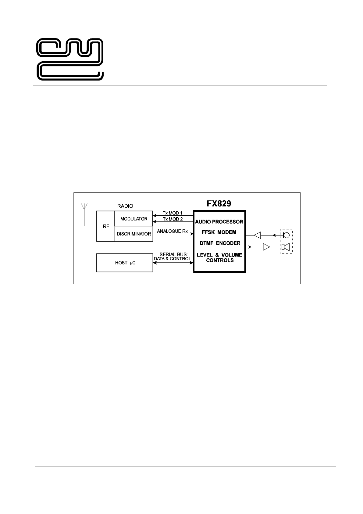
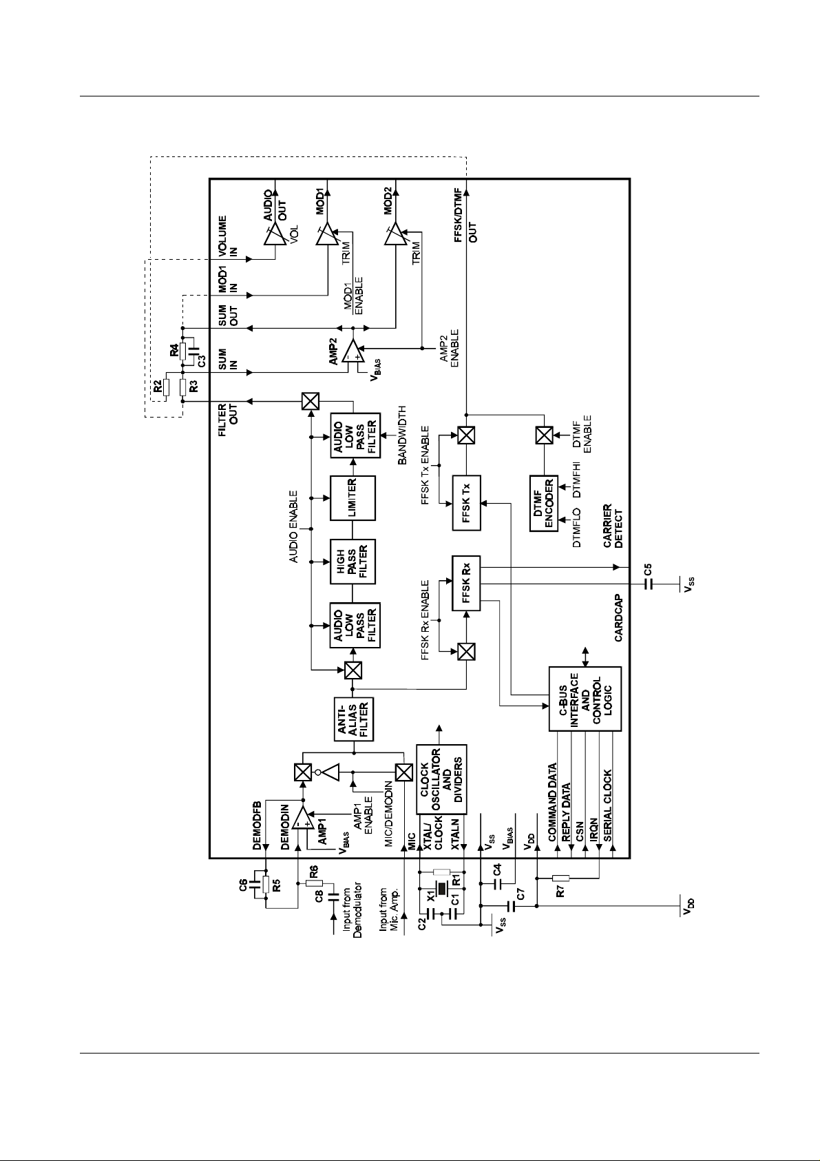
1.2 Block Diagram
Figure 1 Block Diagram
1997 Consumer Microcircuits Limited 3 D/829/4
Page 4

Baseband Signal Processor FX829
1.3 Signal List
Package
D2/D5
Signal Description
Pin No. Name Type
1 XTALN O/P The inverted output of the on-chip oscillator.
2 XTAL/CLOCK I/P The input to the on-chip oscillator, for external
Xtal circuit or clock.
3 SERIAL CLOCK I/P The "C-BUS" serial clock input. This clock,
produced by the µController, is used for transfer
timing of commands and data to and from the
device. See "C-BUS" Timing Diagram.
4 COMMAND DATA I/P The "C-BUS" serial data input from the
µController. Data is loaded into this device in
8-bit bytes, MSB (B7) first, and LSB (B0) last,
synchronised to the SERIAL CLOCK. See
"C-BUS" Timing Diagram.
5 REPLY DATA O/P The "C-BUS" serial data output to the
µController. The transmission of REPLY DATA
bytes is synchronised to the SERIAL CLOCK
under the control of the CSN input. This 3-state
output is held at high impedance when not
sending data to the µController. See "C-BUS"
Timing Diagram.
6 CSN I/P The "C-BUS" data loading control function: this
input is provided by the µController. Data
transfer sequences are initiated, completed or
aborted by the CSN signal. See "C-BUS"
Timing Diagram.
7 IRQN O/P This output indicates an interrupt condition to
the µController by going to a logic "0". This is a
"wire-ORable" output, enabling the connection of
up to 8 peripherals to 1 interrupt port on the
µController. This pin has a low impedance
pulldown to logic "0" when active and a highimpedance when inactive. An external pullup
resistor is required.
The conditions that cause interrupts are
indicated in the STATUS register and are
effective if not masked out by a corresponding
bit in the CONTROL register.
8 CARRIER DETECT O/P The carrier detect output for the FFSK Rx.
1997 Consumer Microcircuits Limited 4 D/829/4
Page 5

Baseband Signal Processor FX829
1.3 Signal List (continued)
Package
D2/D5
Signal Description
Pin No. Name Type
9 CARDCAP O/P The carrier detect integrating capacitor.
10 V
BIAS
O/P A bias line for the internal circuitry, held at
. This pin must be decoupled by a
½ V
DD
capacitor mounted close to the device pins.
11 MIC I/P The ac coupled Tx audio input (external
amplification is required for use as a microphone
input).
12 V
ss
Power The negative supply rail (ground).
13 DEMODIN I/P The ac coupled inverting input to the Rx input
amplifier (AMP1).
14 DEMODFB O/P The output of the Rx input amplifier (AMP1) and
the input to the audio filter/limiter section.
15 FILTER OUT O/P Output of the audio filter/limiter section. In
powersave mode this output is connected to
via a 500kΩ resistor.
V
BIAS
16 FFSK/DTMFOUT O/P The 1200 or 2400 baud FFSK Tx output and the
DTMF encoder output. When enabled but not
transmitting FFSK or DTMF signals, or when in
powersave mode, this output is connected to
via a 500kΩ resistor.
V
BIAS
On power-up, this output can be any level: a
General Reset command is required to ensure
that this output attains V
BIAS
initially.
17 SUM IN I/P Input to the audio summing amplifier (AMP2).
18 SUM OUT O/P Output of the audio summing amplifier (AMP2).
19 MOD1 IN I/P Input to MOD1 audio gain control.
20 VOL IN I/P Input to the audio volume control.
21 AUDIO OUT O/P Output of the audio volume control.
22 MOD1 O/P Output of MOD1 audio gain control.
1997 Consumer Microcircuits Limited 5 D/829/4
Page 6

Baseband Signal Processor FX829
1.3 Signal List (continued)
Package
D2/D5
Signal Description
Pin No. Name Type
23 MOD2 O/P Output of MOD2 audio gain control.
24 V
DD
Power The positive supply rail. Levels and voltages are
dependent upon this supply. This pin should be
decoupled to V
by a capacitor.
SS
Notes: I/P = Input
O/P = Output
1997 Consumer Microcircuits Limited 6 D/829/4
Page 7
Baseband Signal Processor FX829
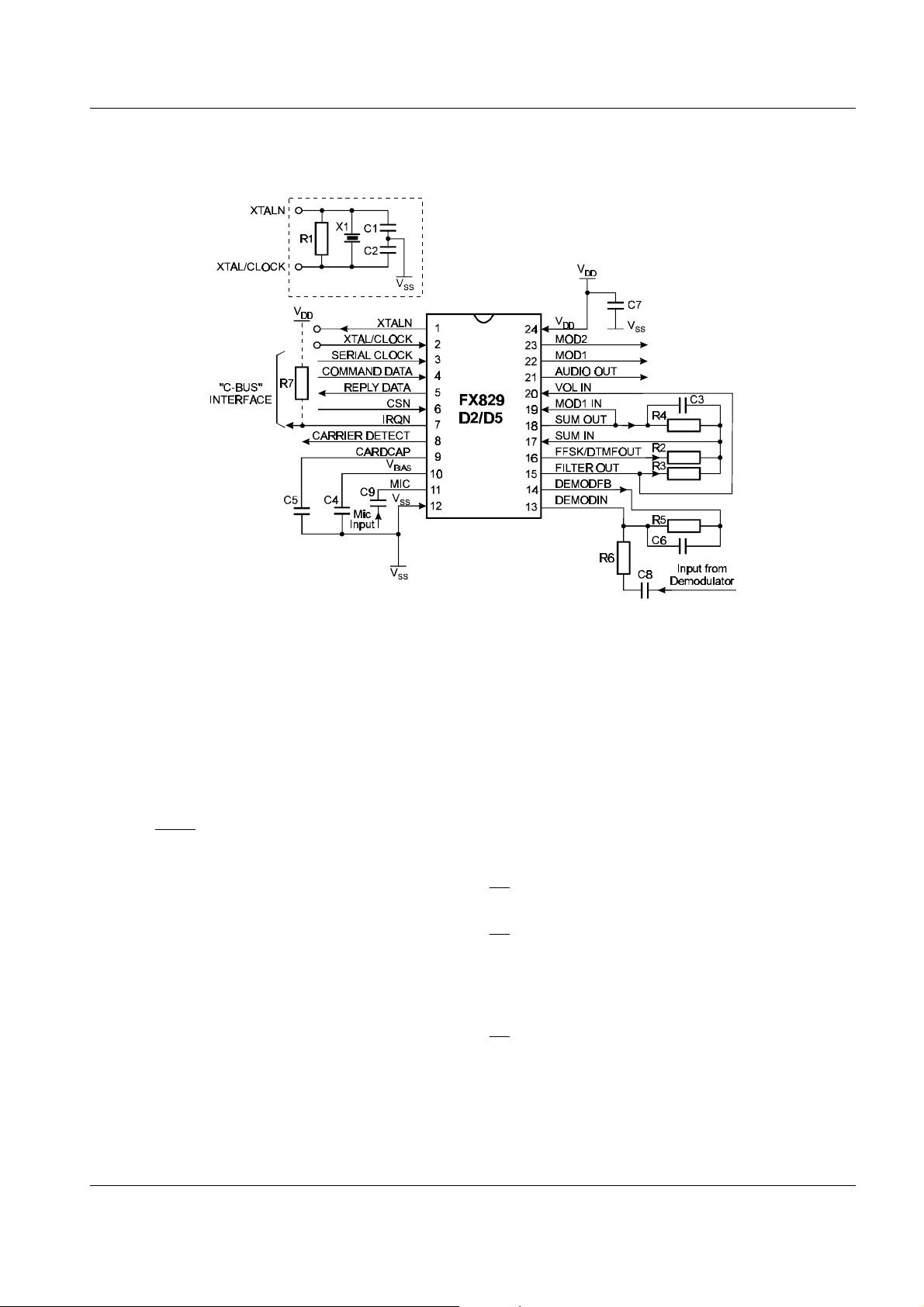
1.4 External Components
C1 22pF ±20% R1 1MW ±5% X1 4.032MHz ±100ppm
C2 22pF ±20% R2 Note 1 ±10%
C3 68pF ±20% R3 Note 1 ±10%
C4 0.1µF ±20% R4 100k
C5 0.1µF ±10% R5 100k
W ±10%
W ±10%
C6 100pF ±20% R6 Note 2 ±10%
C7 0.1µF ±20% R7 22k
W ±10%
C8 Note 2 ±20%
C9 5.6nF ±20%
Notes: 1. R2, R3, R4 and C3 form the gain components for the Summing Amplifier (AMP2).
R2 and R3 should be chosen as required from the system specification, using the
following formulae:
Audio Gain =
DTMF Gain=
R4
−
R3
R4
−
R2
2. R5, R6, C6 and C8 form the gain components for the Rx Input Amplifier (AMP1).
R6 should be chosen as required by the signal level, using the following formula:
Gain =
R5
−
R6
C8 x R6 should be chosen so as not to compromise the low frequency performance of
this product.
Figure 2 Recommended External Components
1997 Consumer Microcircuits Limited 7 D/829/4
Page 8

Baseband Signal Processor FX829
1.5 General Description
The FX829 consists of five main sections: the audio filter section, the programmable attenuators, the
DTMF encoder, the FFSK transmitter and the FFSK receiver. All these sections are controlled via a
serial ("C-BUS") interface. The four sections are described below.
Audio Filtering
This consists of an input amplifier and a common audio filter section, which may be switched between
Rx and Tx. The filter section comprises an anti-alias filter followed by low-pass and high-pass filtering
with an amplitude limiter to set the maximum deviation. Three variable attenuation blocks may be
used to set the volume (in Rx) or the modulation level (in Tx). Pre- and de-emphasis can be added
externally using resistors and capacitors around AMP1, AMP2 and the microphone amplifiers, see
Figure 7. The anti-alias filter is designed to reduce aliasing effects above 50kHz which is
approximately half the internal filter's sample rate.
The filtering is designed to meet the ETS 300 086 specification.
Various powersave modes are incorporated.
MOD1 and MOD2 Attenuators
The MOD1 input can be connected directly to SUM OUT, so that the MOD1 and MOD2 outputs can
then be used for two point modulation. Alternatively, the MOD1 attenuator can be used for auxiliary
gain adjustment, in which case the input signal must be ac coupled with a suitable capacitor.
DTMF Encoder
This generates the standard DTMF tones according to the CONTROL 2 Register settings. It also has
a powersave mode.
FFSK Tx
The Tx function of the FFSK modem operates continuously in a free format mode, which means that
the preamble and frame sync have to be programmed like normal data bytes. However, a 2-byte
checksum may be generated automatically by simply marking the beginning and end of the data to be
used. Any number of whole bytes may be used to generate the checksum.
After the last byte has been transmitted one additional "hang bit" is automatically added to the end. All
Tx operations are programmed from the "C-BUS" via an 8-bit buffer. The Tx part of the FFSK modem
has a powersave mode.
The modulation output is one cycle of 1200Hz for a "1" and one and a half cycles of 1800Hz for a "0"
at 1200 baud, or one half cycle of 1200Hz for a "1" and one cycle of 2400Hz for a "0" at 2400 baud.
FFSK Rx
In Rx, the modem automatically achieves bit sync and then recognises the previously selected SYNC
and/or SYNT word of the MPT1327, ETS 300 230 or PAA1382 specifications. At the same time as
the above, it can also recognise a user programmed 16-bit RX SYNC WORD.
On reception of the SYNC, SYNT or RX SYNC WORD, the device will automatically (or manually at
any time) start checking the data and checksum. It provides a 1-bit correct/incorrect result every byte,
so that any number of bytes can be checked.
The Rx part of the FFSK modem operates at 1200 or 2400 baud and has a powersave mode. Both
FFSK Rx and Tx work in half duplex mode.
1997 Consumer Microcircuits Limited 8 D/829/4
Page 9

Baseband Signal Processor FX829
1.5.1 Software Description
Address/Commands
Instructions and data are transferred, via "C-BUS", in accordance with the timing information given in
Figure 11.
Instruction and data transactions to and from the FX829 consist of an Address/Command (A/C) byte
followed by either:
(i) a further instruction or data (1 or 2 bytes) or
(ii) a status or Rx data reply (1 byte)
8-bit Write Only Registers
HEX
ADDRESS/
COMMAND
$01 RESET N/A N/A N/A N/A N/A N/A N/A N/A
$10 CONTROL 1 AMP1 AMP2 AUDIO FFSKRX FFSKTX UK/F MIC B/W
$11 CONTROL 2 CHKSUM DTMFEN DTMFHI DTMFLO DTMF3 DTMF2 DTMF1 DTMF0
REGISTER
NAME
BIT 7
(D7)
BIT 6
(D6)
BIT 5
(D5)
BIT 4
(D4)
BIT 3
(D3)
BIT 2
(D2)
BIT 1
(D1)
BIT 0
(D0)
$13 AUDIO
ATTENUATION 0 0 0 BIT 4 BIT 3 BIT 2 BIT 1 BIT 0
$40 CONTROL 3/
IRQ ENABLE
$43 TXDATA
0 1200/2400 TXIDLEM RXDATAM TXDATAM
<----------------------------------------------- TXDATA ----------------------------------------------->
BIT 7 BIT 6 BIT 5 BIT 4 BIT 3 BIT 2 BIT 1 BIT 0
<-------------------------- GAIN -------------------------->
RX SYNC
WORD
PRIME
SYNT
PRIME
16-bit Write Only Registers
HEX
ADDRESS/
COMMAND
$12 MOD LEVELS MOD 1 <-------------------------- MOD 1 -------------------------->
$44 RX SYNC <------------------------------------------- RX SYNC WORD ----------------------------------------->
REGISTER
NAME
(1) 0 0 ENABLE BIT 4 BIT 3 BIT 2 BIT 1 BIT 0
(2) 0 0 0 BIT 4 BIT 3 BIT 2 BIT 1 BIT 0
WORD (1) BIT 15 BIT 14 BIT 13 BIT 12 BIT 11 BIT 10 BIT 9 BIT 8
(2) BIT 7 BIT 6 BIT 5 BIT 4 BIT 3 BIT 2 BIT 1 BIT 0
BIT 7
(D7)
<------------------------------------------- RX SYNC WORD ----------------------------------------->
BIT 6
(D6)
BIT 5
(D5)
BIT 4
(D4)
<-------------------------- MOD 2 -------------------------->
BIT 3
(D3)
BIT 2
(D2)
BIT 1
(D1)
SYNC
PRIME
BIT 0
(D0)
Write Only Register Description
RESET Register (Hex address $01)
The reset command has no data attached to it. It sets the device registers into the specific states as listed
below:
1997 Consumer Microcircuits Limited 9 D/829/4
Page 10

Baseband Signal Processor FX829
REGISTER NAME BIT 7
(D7)
CONTROL 1 0 0 0 0 0 0 0 0
CONTROL 2 0 0 0 0 0 0 0 0
CONTROL 3/IRQ ENABLE 0 0 0 0 0 0 0 0
AUDIO ATTENUATION 0 0 0 0 0 0 0 0
TXDATA X X X X X X X X
MOD LEVELS (1) 0 0 0 0 0 0 0 0
MOD LEVELS (2) 0 0 0 0 0 0 0 0
RX SYNC WORD (1) X X X X X X X X
RX SYNC WORD (2) X X X X X X X X
STATUS 0 0 0 0 0 0 0 0
RXDATA X X X X X X X X
BIT 6
(D6)
BIT 5
(D5)
BIT 4
(D4)
BIT 3
(D3)
BIT 2
(D2)
BIT 1
(D1)
X = undefined
CONTROL1 Register (Hex address $10)
This register is used to control the functions of the device as described below:
AMP1
(Bit 7)
AMP2
(Bit 6)
When this bit is "1", AMP1 is enabled.
When this bit is "0", AMP1 is disabled (i.e. powersaved).
When this bit is "1", both AMP2 and MOD2 are enabled.
When this bit is "0", both AMP2 and MOD2 are disabled (i.e. powersaved) and the
MOD2 output is pulled to V
via a 1MW resistor.
BIAS
BIT 0
D0)
AUDIO
(Bit 5)
FFSKRX
(Bit 4)
FFSKTX
(Bit 3)
UK/F
(Bit 2)
When this bit is "1", the audio filter/limiter section is enabled.
When this bit is "0", the audio filter/limiter section is disabled (i.e. powersaved).
When this bit is "1", the FFSK Rx is enabled.
When this bit is "0", the FFSK Rx is disabled (i.e. powersaved).
Note:
1. The FFSK Rx and Tx cannot both be enabled at the same time. If both
FFSKRX and FFSKTX are "1", then they will both be disabled
(i.e. powersaved).
When this bit is "1", the FFSK Tx is enabled.
When this bit is "0", the FFSK Tx is disabled (i.e. powersaved).
Note:
1. The FFSK Tx and Rx cannot both be enabled at the same time. If both
FFSKTX and FFSKRX are "1", then they will both be disabled
(i.e. powersaved).
2. The DTMF Encoder and FFSK Tx cannot both be enabled at the same time.
If both DTMFEN and FFSKTX are "1", then they will both be disabled.
When this bit is "1", the SYNC/SYNT is set to the PAA standard of
"1011010000110011" (SYNC)
When this bit is "0", the SYNC/SYNT is set to the MPT standard of
"1100010011010111" (SYNC)
1997 Consumer Microcircuits Limited 10 D/829/4
Page 11

Baseband Signal Processor FX829
MIC
(Bit 1)
When this bit is "1", the MIC input is enabled and the AMP1 (DEMODIN) input is
disabled.
When this bit is "0", the AMP1 (DEMODIN) input is enabled and the MIC input is
disabled.
B/W
(Bit 0)
When this bit is "1", the bandwidth of the audio path is set wide for 20kHz/25kHz
RF channel spacing.
When this bit is "0", the bandwidth of the audio path is set narrow for 12.5kHz RF
channel spacing.
CONTROL 2 Register (Hex address $11)
This register is used to control the functions of the device as described below:
CHKSUM
(Bit 7)
In the Tx mode, when this bit is "1", the checksum generator is enabled. All
complete bytes that are transmitted after this time are used in the checksum
calculation.
When this bit goes from "1" to "0", the checksum generator will complete its
calculations on the current byte and the result will be sent as the next two bytes of
transmitted data.
In the Rx mode, the "0" to "1" transition of the CHKSUM bit is used at the start of
the next byte received at DEMODIN to manually reset the Rx checksum
calculation, see Figure 4. The calculation can also be reset automatically by a
SYNC, SYNT, or RX SYNC WORD detection - see CONTROL 3 / IRQ ENABLE
Register. In this case, the Rx checksum calculation starts with the first data byte
after the 2-byte sync word has been detected. The CHKSUM bit can be reset to
"0" at any time. The result of the checksum is made available in the STATUS
Register after the reception of every complete byte (See RXSUMF bit of the
STATUS Register).
Note that the device is designed to work with any message length, and as a
consequence it is not aware of the position of the checksum within the incoming
data message. It thus performs a checksum assessment after every received
byte. The controlling software should use its knowledge of the system message
length in order to determine which RXSUMF reading is valid, i.e. after the second
of the two checksum bytes has been received.
The timing of data bytes relative to the checksum bit is shown in Figures 3 and 4.
1997 Consumer Microcircuits Limited 11 D/829/4
Page 12

Baseband Signal Processor FX829
Figure 3 Checksum Generation in Tx Mode
Figure 4 Checksum Calculation in Rx Mode
1997 Consumer Microcircuits Limited 12 D/829/4
Page 13

Baseband Signal Processor FX829
DTMFEN
(Bit 6)
DTMFHI
(Bit 5)
DTMFLO
(Bit 4)
DTMF3, DTMF2,
DTMF1, DTMF0
(Bit 3, Bit 2,
Bit 1, Bit 0)
When this bit is "1", the DTMF output is enabled.
When this bit is "0", the DTMF output is disabled. As the powersave of the DTMF
is performed in the DTMFHI and DTMFLO registers, this bit allows a fast start up
time for the tones.
Note:
1. The DTMF Encoder and FFSK Tx cannot both be enabled at the same time.
If both DTMFEN and FFSKTX are "1", then they will both be disabled.
When this bit is "1", the DTMF high frequency tone generator is enabled. It will not
appear on the output pin unless or until the DTMFEN is "1".
When this bit is "0", the DTMF high frequency tone generator is disabled (i.e.
powersaved).
When this bit is "1", the DTMF low frequency tone generator is enabled. It will not
appear on the output pin unless or until the DTMFEN is "1".
When this bit is "0", the DTMF low frequency tone generator is disabled (i.e.
powersaved).
These four bits define the DTMF tones according to the table below:
Bit
3
Bit
2
Bit
1
Bit
0
DTMF
Tones
DTMF
0 0 0 0 1209Hz + 697Hz 1
0 0 0 1 1209Hz + 770Hz 4
0 0 1 0 1209Hz + 852Hz 7
0 0 1 1 1209Hz + 941Hz *
0 1 0 0 1337Hz + 697Hz 2
0 1 0 1 1337Hz + 770Hz 5
0 1 1 0 1337Hz + 852Hz 8
0 1 1 1 1337Hz + 941Hz 0
1 0 0 0 1478Hz + 697Hz 3
1 0 0 1 1478Hz + 770Hz 6
1 0 1 0 1478Hz + 852Hz 9
1 0 1 1 1478Hz + 941Hz #
1 1 0 0 1634Hz + 697Hz A
1 1 0 1 1634Hz + 770Hz B
'Digit'
1 1 1 0 1634Hz + 852Hz C
1 1 1 1 1634Hz + 941Hz D
1997 Consumer Microcircuits Limited 13 D/829/4
Page 14

Baseband Signal Processor FX829
AUDIO ATTENUATION Register (Hex Address $13)
The five least significant bits in this register are used to set the attenuation of the audio volume control
according to the table below:
4 3 2 1 0 Audio Attenuation
0 0 0 0 0 Off
0 0 0 0 1 48.0dB
0 0 0 1 0 46.4dB
0 0 0 1 1 44.8dB
0 0 1 0 0 43.2dB
0 0 1 0 1 41.6dB
0 0 1 1 0 40.0dB
0 0 1 1 1 38.4dB
0 1 0 0 0 36.8dB
0 1 0 0 1 35.2dB
0 1 0 1 0 33.6dB
0 1 0 1 1 32.0dB
0 1 1 0 0 30.4dB
0 1 1 0 1 28.8dB
0 1 1 1 0 27.2dB
0 1 1 1 1 25.6dB
1 0 0 0 0 24.0dB
1 0 0 0 1 22.4dB
1 0 0 1 0 20.8dB
1 0 0 1 1 19.2dB
1 0 1 0 0 17.6dB
1 0 1 0 1 16.0dB
1 0 1 1 0 14.4dB
1 0 1 1 1 12.8dB
1 1 0 0 0 11.2dB
1 1 0 0 1 9.6dB
1 1 0 1 0 8.0dB
1 1 0 1 1 6.4dB
1 1 1 0 0 4.8dB
1 1 1 0 1 3.2dB
1 1 1 1 0 1.6dB
1 1 1 1 1 0dB
Bits 5, 6 and 7 should always be set to "0".
CONTROL 3 / IRQ ENABLE Register (Hex address $40)
This register is a mixture of control bits and interrupt mask bits, as detailed below:
Bit 7
1200/2400
(Bit 6)
1997 Consumer Microcircuits Limited 14 D/829/4
Not used, set to zero.
When this bit is "1", the FFSK Rx and Tx are set to operate at 1200 baud.
When this bit it "0", the FFSK Rx and Tx are set to operate at 2400 baud.
Page 15

Baseband Signal Processor FX829
TXIDLEM
(Bit 5)
RXDATAM
(Bit 4)
TXDATAM
(Bit 3)
RX SYNC
WORD PRIME
(Bit 2)
SYNT PRIME
(Bit 1)
SYNC PRIME
(Bit 0)
When this bit is "1", the TXIDLE interrupt will be gated out to the IRQN pin.
When this bit is "0", the TXIDLE interrupt will be inhibited. This bit has no effect on
the contents of the STATUS register.
When this bit is "1", the RXDATA interrupt will be gated out to the IRQN pin.
When this bit is "0", the RXDATA interrupt will be inhibited. This bit has no effect
on the contents of the STATUS register.
When this bit is "1", the TXDATA interrupt will be gated out to the IRQN pin.
When this bit is "0", the TXDATA interrupt will be inhibited. This bit has no effect
on the contents of the STATUS register.
When this bit is set to "1", it enables the RX SYNC WORD detection.
It is cleared/disabled when a SYNC, SYNT, or RX SYNC WORD is detected.
It may also be cleared/disabled by writing "0" directly to this bit.
When this bit is set to "1", it enables the SYNT detection.
It is cleared/disabled when a SYNC, SYNT, or RX SYNC WORD is detected.
It may also be cleared/disabled by writing "0" directly to this bit.
When this bit is set to "1", it enables the SYNC detection.
It is cleared/disabled when a SYNC, SYNT, or RX SYNC WORD is detected.
It may also be cleared/disabled by writing "0" directly to this bit.
TXDATA Register (Hex Address $43)
This is the Tx data output register. It is double buffered, thus giving the user up to 8 bit periods to load in the
next 8 bits. FFSK data is transmitted immediately it is loaded if the transmitter is idle. Data is transmitted in 8bit bytes, bit 7 (MSB) will be transmitted first.
1997 Consumer Microcircuits Limited 15 D/829/4
Page 16

Baseband Signal Processor FX829
MOD LEVELS Register (Hex address $12)
The six least significant bits of the first byte in this register are used to set the attenuation of the Modulator 1
amplifier and the five least significant bits of the second byte in this register are used to set the attenuation of
the Modulator 2 amplifier, according to the tables below:
5 4 3 2 1 0 Mod. 1 Attenuation 4 3 2 1 0 Mod. 2 Attenuation
0 X X X X X Disabled (V
1 0 0 0 0 0 >40dB 0 0 0 0 0 >40dB
1 0 0 0 0 1 12.0dB 0 0 0 0 1 6.0dB
1 0 0 0 1 0 11.6dB 0 0 0 1 0 5.8dB
1 0 0 0 1 1 11.2dB 0 0 0 1 1 5.6dB
1 0 0 1 0 0 10.8dB 0 0 1 0 0 5.4dB
1 0 0 1 0 1 10.4dB 0 0 1 0 1 5.2dB
1 0 0 1 1 0 10.0dB 0 0 1 1 0 5.0dB
1 0 0 1 1 1 9.6dB 0 0 1 1 1 4.8dB
1 0 1 0 0 0 9.2dB 0 1 0 0 0 4.6dB
1 0 1 0 0 1 8.8dB 0 1 0 0 1 4.4dB
1 0 1 0 1 0 8.4dB 0 1 0 1 0 4.2dB
1 0 1 0 1 1 8.0dB 0 1 0 1 1 4.0dB
1 0 1 1 0 0 7.6dB 0 1 1 0 0 3.8dB
1 0 1 1 0 1 7.2dB 0 1 1 0 1 3.6dB
1 0 1 1 1 0 6.8dB 0 1 1 1 0 3.4dB
1 0 1 1 1 1 6.4dB 0 1 1 1 1 3.2dB
1 1 0 0 0 0 6.0dB 1 0 0 0 0 3.0dB
1 1 0 0 0 1 5.6dB 1 0 0 0 1 2.8dB
1 1 0 0 1 0 5.2dB 1 0 0 1 0 2.6dB
1 1 0 0 1 1 4.8dB 1 0 0 1 1 2.4dB
1 1 0 1 0 0 4.4dB 1 0 1 0 0 2.2dB
1 1 0 1 0 1 4.0dB 1 0 1 0 1 2.0dB
1 1 0 1 1 0 3.6dB 1 0 1 1 0 1.8dB
1 1 0 1 1 1 3.2dB 1 0 1 1 1 1.6dB
1 1 1 0 0 0 2.8dB 1 1 0 0 0 1.4dB
1 1 1 0 0 1 2.4dB 1 1 0 0 1 1.2dB
1 1 1 0 1 0 2.0dB 1 1 0 1 0 1.0dB
1 1 1 0 1 1 1.6dB 1 1 0 1 1 0.8dB
1 1 1 1 0 0 1.2dB 1 1 1 0 0 0.6dB
1 1 1 1 0 1 0.8dB 1 1 1 0 1 0.4dB
1 1 1 1 1 0 0.4dB 1 1 1 1 0 0.2dB
1 1 1 1 1 1 0dB 1 1 1 1 1 0dB
BIAS
)
X = don't care
MOD1 ENABLE
(Bit 5, first byte)
When this bit is "1" the MOD1 attenuator is enabled.
When this bit is "0" the MOD1 attenuator is disabled (i.e. powersaved).
Bits 6 and 7 in the first byte and bits 5, 6 and 7 in the second byte should always
be set to "0". MOD LEVELS (1) register is loaded first.
Note: The MOD2 attenuator is enabled by the AMP2 ENABLE signal (bit 6 of
CONTROL1 register).
RX SYNC WORD Register (Hex $44)
This is a two byte register that defines the 16-bit programmable synchronisation word. This word is compared
with the incoming Rx data and, if a match is found, it is indicated in the STATUS register and an interrupt is
generated. Bit 15, the MSB of the first byte, is loaded first.
1997 Consumer Microcircuits Limited 16 D/829/4
Page 17

Baseband Signal Processor FX829
8-bit Read Only Registers
HEX
ADDRESS/
COMMAND
$41 STATUS 0 RXSUMF TXIDLEF RXDATAF TXDATAF RX SYNC
$42 RXDATA <--------------------------------------------- RXDATA --------------------------------------------->
REGISTER
NAME
BIT 7
(D7)
BIT 7 BIT 6 BIT 5 BIT 4 BIT 3 BIT 2 BIT 1 BIT 0
BIT 6
(D6)
BIT 5
(D5)
BIT 4
(D4)
BIT 3
(D3)
BIT 2
(D2)
WORDF
BIT 1
(D1)
SYNTF SYNCF
BIT 0
(D0)
Read Only Register Description
STATUS Register (Hex address $41)
This register is used to indicate the status of the device as described below:
Bit 7
RXSUMF
(Bit 6)
TXIDLEF
(Bit 5)
RXDATAF
(Bit 4)
TXDATAF
(Bit 3)
RX SYNC
WORDF
(Bit 2)
Not used, always set to zero.
When this bit is "1", the Rx checksum is correct.
When this bit is "0", the Rx checksum is incorrect.
This bit is updated and latched in after reception of every eight bits (see CHKSUM
bit of the CONTROL2 register).
When all the Tx data and any checksum and one "hang-bit" have been transmitted,
this bit will be set to "1" to indicate that the transmitter is idle. This bit is reset to
"0" immediately after reading the STATUS register. When this bit is set to "1", an
interrupt may be generated depending on the state of the TXIDLEM bit in the
CONTROL 3 / IRQ ENABLE register.
When a full byte of data is received and is available in the RXDATA register, this
bit will be set to "1". This bit is reset to "0" immediately after reading the STATUS
register. When this bit is set to "1" an interrupt may be generated depending on
the state of the RXDATAM bit in the CONTROL 3 / IRQ ENABLE register.
When the Tx data buffer is empty this bit will be set to "1".
This bit is reset to "0" immediately after reading the STATUS register. When this
bit is set to "1", an interrupt may be generated depending on the state of the
TXDATAM bit in the CONTROL 3 / IRQ ENABLE register.
This bit is only defined when RX SYNC WORD PRIME is enabled.
When the data sequence specified in the RX SYNC WORD register has been
successfully matched to the Rx incoming data, this bit will be set to "1".
This bit is reset to "0" immediately after reading the STATUS register. When this
bit is set to "1", an interrupt will be generated, the checksum generator and byte
counter will be reset and SYNC PRIME, SYNT PRIME and RX SYNC WORD
PRIME will be reset.
SYNTF
(Bit 1)
This bit is only defined when SYNT PRIME is enabled.
When the data sequence specified by SYNT has been successfully matched to the
Rx incoming data, this bit will be set to "1".
This bit is reset to "0" immediately after reading the STATUS register. When this
bit is set to "1", an interrupt will be generated, the checksum generator and byte
counter will be reset and SYNC PRIME, SYNT PRIME and RX SYNC WORD
PRIME will be reset.
1997 Consumer Microcircuits Limited 17 D/829/4
Page 18

Baseband Signal Processor FX829
SYNCF
(Bit 0)
This bit is only defined when SYNC PRIME is enabled.
When the data sequence specified by SYNC has been successfully matched to the
Rx incoming data, this bit will be set to "1".
This bit is reset to "0" immediately after reading the STATUS register. When this
bit is set to "1", an interrupt will be generated, the checksum generator and byte
counter will be reset and SYNC PRIME, SYNT PRIME and RX SYNC WORD
PRIME will be reset.
RXDATA Register (Hex address $42)
This register contains the last byte of data received. It is updated every 8 bits at the same time as the
RXSUMF bit in the STATUS register is updated.
The RXDATA register is double buffered, thus giving the user up to 8 bit periods to read the data before it is
overwritten by the next byte.
1.5.2 FFSK Checksum Generation and Checking
Generation
The checksum generator takes the m x 8 bits from the m bytes of information, sequentially loaded into
the TXDATA register and divides them modulo-2, by the generating polynomial:
15
+ X14 + X13 + X11 + X4 + X2 + 1
X
It then takes the 15-bit remainder from the polynomial divider, inverts the last bit and appends an
EVEN parity bit generated from the initial m x 8 bits and the 15-bit remainder (with the last bit
inverted).
This 16-bit word is used as the "CHECKSUM". See Figure 5.
(m = the number of bytes in the information to be sent)
Figure 5 Checksum Generation
1997 Consumer Microcircuits Limited 18 D/829/4
Page 19

Baseband Signal Processor FX829
Checking
The checksum checker performs two tasks:
It takes the first n-1 bits of a received (n = 8m + 16 bits) message, inverts bit n-1, and divides them
modulo-2, by the generating polynomial:
15
+ X14 + X13 + X11 + X4 + X2 + 1
X
The 15 bits remaining in the polynomial divider are checked for all zero.
Secondly, it generates an EVEN parity bit from the first n-1 bits of a received message and compares
this bit with the received parity bit (bit n). See Figure 6.
If the 15 bits in the polynomial divider are all zero, and the two parity bits are equal, then the RXSUMF
bit (STATUS register bit 6) is set. This is updated and latched every 8 bits, starting at the bit
immediately after the initialisation of the bit counter. This initialisation takes place on detection of
frame synchronisation, i.e. the matching of received data to the SYNC, SYNT or RX SYNC WORD.
Note that the checksum is calculated on the received data before it is double buffered (see Figure 4).
n = the number of bits in the received message
m = the number of bytes of transmitted data, excluding checksum
Figure 6 Checksum Checking
1997 Consumer Microcircuits Limited 19 D/829/4
Page 20

Baseband Signal Processor FX829
1.6 Application Notes
The following block diagrams show the possible arrangements for the pre- and de-emphasis required
by PAA1382 and MPT1327 specifications.
Figure 7a Transmitter Pre-emphasis
(showing both pre-emphasis positions, as required by the PAA1382 specification.
Remove pre-emphasis 2 for the MPT1327 specification requirement)
Figure 7b PAA1382 Receiver De-emphasis
(showing position of de-emphasis in all paths, as required by the PAA1382 specification)
Figure 7c MPT1327 Receiver De-emphasis
(showing position of de-emphasis in audio path only, as required by the MPT1327 specification)
1997 Consumer Microcircuits Limited 20 D/829/4
Page 21

Baseband Signal Processor FX829
The FX829 should be programmed in the following manner:
1. Perform a General Reset when first applying power to the FX829.
2. Program the FX829 configuration whilst in powersave.
e.g. UK/F, MIC, B/W, 1200/2400, DTMF0-3,
DTMFHI, DTMFLO, TXIDLEM, RXDATAM, TXDATAM,
RX SYNC WORD PRIME, SYNT PRIME, SYNC PRIME,
MOD1, MOD2, RX SYNC WORD and AUDIO ATTENUATOR.
3. Take the appropriate parts of the FX829 out of powersave by enabling:
AMP1, AMP2, MOD1, MOD2, AUDIO and (DTMFEN or FFSKTX or FFSKRX).
4. In DTMF Tx mode, a DTMF tone will be generated for the duration that DTMFEN is set to “1”.
5. In FFSK Rx mode, wait for an interrupt (IRQN = “0”) or poll the STATUS register. Remember
that all status flags are reset after reading the STATUS register.
(a) If RXSYNCWORDF, SYNTF or SYNCF become set to “1”, the corresponding
synchronisation word has been detected. This indicates the start of valid Rx data. The
checksum calculation will be automatically reset. Note that the timing of RXDATAF will be
re-aligned by the generation of a SYNC, SYNT or RX SYNC WORD interrupt.
(b) When RXDATAF subsequently becomes set to “1”, read the Rx data from the RXDATA
register. (Note that RXDATAF will be set every 8 bits regardless of whether valid Rx data is
being received or not. Sync and checksum patterns should be considered for validating the
data).
(c) If RXSUMF becomes set to “1”, then all of the Rx data sent (starting after the
synchronisation word and terminating with a checksum) will have been correctly received.
Note that it is necessary to know in advance what message length is expected, in order to
determine at which point RXSUMF is valid (i.e. after the interrupt for the second checksum
data byte being received has occurred). The RXSUMF bit is invalid at all other times. When
RXSUMF becomes set to “1”, the last two bytes of Rx data received will represent the twobyte checksum transmitted. The first checksum byte will already have been read from the
RXDATA register, the last byte is available to be read, as the RXDATAF bit will also have
been set to “1”.
6. In FFSK Tx mode, wait for an interrupt (IRQN = “0”) or poll the STATUS register. Remember that
all status flags are reset after reading the STATUS register.
(a) Do not send Tx data until the TXDATAF bit has been set to “1”. When the TXDATAF bit is
next set to “1”, write the first byte of Tx data to the TXDATA register. If the transmit buffer is
empty, this data will be transmitted immediately, causing the TXDATAF bit to be set to “1”
approximately one FFSK bit-period after the TXDATA register has been loaded with data.
(Any TXIDLEF bit set upon entering FFSK Tx mode should be ignored).
(b) The next byte of Tx data should be written to the TXDATA register as soon as the TXDATAF
bit has been set to “1”. Once this has been done, the TXDATAF bit will again be set to “1”
eight FFSK bit-periods after the TXDATA register was loaded with the second byte of data.
1997 Consumer Microcircuits Limited 21 D/829/4
Page 22

Baseband Signal Processor FX829
(c) Subsequent bytes of Tx data should be written to the TXDATA register as soon as the
TXDATAF bit has been set to”1”. After the last byte of Tx data has been loaded, the
TXDATAF bit will be set after both 8 and 16 FFSK bit-periods followed by the TXIDLEF bit
which will be set approximately one FFSK bit-period later, to indicate that the final bit has
been transmitted.
(d) The TXDATAF bit will continue to be set every 8 FFSK bit-periods, regardless of whether Tx
data is written to the TXDATA register or not, providing the transmitter is enabled (FFSK Tx
mode = FFSKTX bit set to “1”). Note that whilst the 2-byte checksum is being generated and
transmitted, the TXDATAF bit will not be set for approximately 24 FFSK bit-periods.
1997 Consumer Microcircuits Limited 22 D/829/4
Page 23

Baseband Signal Processor FX829
Figure 8 Reception of 2 Bytes of Data
1997 Consumer Microcircuits Limited 23 D/829/4
Page 24

Baseband Signal Processor FX829
Figure 9 Transmission of 3 Bytes of Data
1997 Consumer Microcircuits Limited 24 D/829/4
Page 25

Baseband Signal Processor FX829
1.7 Performance Specification
1.7.1 Electrical Performance
Absolute Maximum Ratings
Exceeding these maximum ratings can result in damage to the device.
Min. Max. Units
Supply (VDD - VSS) -0.3 7.0 V
Voltage on any pin to V
Current into or out of V
SS
DD
and V
pins -30 +30 mA
SS
Current into or out of any other pin -20 +20 mA
D2 Package Min. Max. Units
Total Allowable Power Dissipation at Tamb = 25°C 800 mW
... Derating 13 mW/°C
Storage Temperature -40 +85 °C
Operating Temperature -40 +85 °C
-0.3 V
+ 0.3 V
DD
D5 Package Min. Max. Units
Total Allowable Power Dissipation at Tamb = 25°C 550 mW
... Derating 9 mW/°C
Storage Temperature -40 +85 °C
Operating Temperature -40 +85 °C
Operating Limits
Correct operation of the device outside these limits is not implied.
Notes Min. Max. Units
Supply (VDD - VSS) 3.0 5.5 V
Operating Temperature -40 +85 °C
Xtal Frequency 4.0315968 4.0324032 MHz
1997 Consumer Microcircuits Limited 25 D/829/4
Page 26

Baseband Signal Processor FX829
Operating Characteristics
For the following conditions unless otherwise specified:
Xtal Frequency = 4.032MHz, Bit Rate = 1.2k bits/sec, Noise Bandwidth = Bit Rate,
Audio Level 0dB ref = 308mVrms at 1kHz
= 3.3V to 5.0V, Tamb = -40°C to +85°C.
V
DD
Notes Min. Typ. Max. Units
DC Parameters
IDD (Powersaved) (VDD = 5.0V) 2 - 0.6 1.5 mA
(Tx or Rx Voice) (VDD = 5.0V) 2 - 5.0 8.0 mA
I
DD
(Powersaved) (VDD = 3.3V) 2 - 0.3 1.0 mA
I
DD
(Tx or Rx Voice) (VDD = 3.3V) 2 - 2.7 4.0 mA
I
DD
"C-BUS" Interface
Input Logic "1" 70% - - V
Input Logic "0" - - 30% V
DD
DD
Input Leakage Current (logic "1" or "0") -1.0 - 1.0 µA
Input Capacitance - - 7.5 pF
Output Logic "1" (I
Output Logic "0" (IOL = 360µA) 10% V
= 120µA) 90% V
OH
DD
DD
"Off" State Leakage Current (Vout = VDD) 9 - - 10 µA
AC Parameters
Input Sensitivity (for 0dB output)
Tx Audio Input (MIC) 8 - 308 - mVrms
Rx Audio Input (DEMODFB) 8 - 308 - mVrms
Output Drive Level
For 60% Deviation 1, 6, 8 291 308 326 mVrms
For 100% Deviation 1, 6, 7, 8 - 1440 - mVpk-pk
Audio Filters
Gain at 1kHz 5 - 0 - dB
Passband Ripple 5 -2.0 - 0.5 dB
SINAD 5, 14 - 59 - dBp
Signal Path Noise 5 - -55 - dB
Narrrow Audio Bandwidth Setting
Passband Frequencies 5 300 - 2550 Hz
Stopband Attenuation: (f = 100Hz) 5 - 3.0 - dB
(f = 3400Hz) 5 - 5.5 - dB
(f = 6000Hz) 5 10.5 24 - dB
(f = 12500Hz) 5 25 49 - dB
Wide Audio Bandwidth Setting
Passband Frequencies 5 300 - 3000 Hz
Stopband Attenuation: (f = 100Hz) 5 - 3.0 - dB
(f = 3400Hz) 5 - 3.0 - dB
(f = 6000Hz) 5 10.5 19 - dB
(f = 25000Hz) 5 39.5 68 - dB
1997 Consumer Microcircuits Limited 26 D/829/4
Page 27

Baseband Signal Processor FX829
Notes Min. Typ. Max. Units
Amp 1 and Amp 2
Open Loop Gain (I/P = 1mV at 100Hz) - 70 - dB
Unity Gain Bandwidth - 5.0 - MHz
Input Impedance (at 100Hz) 10 - Output Impedance (Open Loop) - 6.0 -
(Closed Loop) - 600 -
M
Ω
Ω
k
Ω
Distortion (DTMF) - 2 5 %
FFSK/DTMF TX OUT
Tx O/P impedance (not powersaved) 3 1.0 2.5
Tx O/P impedance (powersaved) 3 300 500 -
Ω
k
Ω
k
Signal Level (FFSK) 1 -1 0 +1 dB
Signal Level (DTMF High Tone) 1 - +2.0 - dB
Signal Level (DTMF Low Tone) 1 - 0 - dB
Distortion (DTMF) - 2 5 %
FFSK TX OUT
Isochronous Distortion:
(1200Hz - 1800Hz) 25 40 µs
(1800Hz - 1200Hz) 25 40 µs
(1200Hz - 2400Hz) 20 30 µs
(2400Hz - 1200Hz) 20 30 µs
Third Harmonic Distortion 2 3 %
Deviation Limiter
Threshold 1 - 1300 - mVpk-pk
Gain -0.5 - 0.5 dB
Transmitter Modulator Drives
Input Impedance
(MOD1 IN, VOLUME IN) (at 100Hz) - 15.0 -
Ω
k
Mod.1 Attenuator
Nominal Adjustment Range 0 12.0 dB
Attenuation Accuracy -1.0 - 1.0 dB
Step Size 0.2 0.4 0.6 dB
Output Impedance 3 - 600 -
Ω
Mod.2 Attenuator
Nominal Adjustment Range 0 6.0 dB
Attenuation Accuracy -0.6 - 0.6 dB
Step Size 0.1 0.2 0.3 dB
Output Impedance 3 - 600 -
Ω
Audio Output Attenuator
Nominal Adjustment Range 0 48.0 dB
Attenuation Accuracy -1.5 - 1.5 dB
Step Size - 1.6 - dB
Output Impedance 3 - 600 -
Ω
1997 Consumer Microcircuits Limited 27 D/829/4
Page 28

Baseband Signal Processor FX829
Notes Min. Typ. Max. Units
FFSK Receiver
Signal Input Dynamic Range (SNR = 50dB) 10, 11 100 230 1000 mVrms
Bit Error Rate
4
(SNR = 12dB at 1200 Baud) 11 - 2.5 - 10
(SNR = 12dB at 2400 Baud) 11 - 1.5 - 10
(SNR = 20dB at 1200/2400 Baud) 11 - 1.0 - 10
-
-
3
-
8
Receiver Synchronisation (SNR = 12dB) 12
Probability of Bit 16 being correct 0.995
Carrier Detect
Sensitivity 12, 13 - - 150 mVrms
Probability of Carrier Detection
- After Bit 16 (SNR = 12dB) 0.995
- With 230mVrms Noise (No Signal) 0.05
Miscellaneous Impedances
FILTER OUT - 600 Tx Audio Input (MIC) (at 100Hz) 10 - -
M
Ω
Ω
Xtal/Clock Input
'High' pulse width 4 40 ns
'Low' pulse width 4 40 ns
Input Impedance (at 100Hz) 10
Gain (I/P = 1mVrms at 100Hz) 20 dB
Notes: 1. At VDD = 5.0V only. Signal levels are proportional to VDD.
2. Not including any current drawn from the modem pins by external circuitry.
Powersaved = all functions disabled.
Tx or Rx = device configured into any half-duplex operating mode.
Currents measured at Tamb = 25°C only.
3. Small signal impedance, at V
= 5.0V and Tamb = 25°C. A minimum load resistance of 6kΩ
DD
is suggested.
4. Timing for an external input to the XTAL/CLOCK pin.
5. Between MIC or AMP1 inputs to Modulator and Audio outputs, see Figures 10a and 10b.
6. It is recommended that these output levels are used to produce 60% or 100% deviation in the
transmitter.
7. With the Tx Audio input level 20dB above the level required to produce 0dB at the
Output Drives.
8. With output gains set to 0dB.
9. IRQN pin.
10. See Figure 13 (variation of BER with Input Signal Level).
11. SNR = Signal to Noise Ratio in the Bit Rate Bandwidth.
12. For a "10101010101 ...01" pattern.
13. Measured with a 150mVrms input signal (no noise).
14. dBp represents a psophometrically weighted measurement.
M
Ω
1997 Consumer Microcircuits Limited 28 D/829/4
Page 29

Baseband Signal Processor FX829
10
Res pon s e must not exceed thi s li mit
0
0.5dB
-2dB
-10.5 dB
-10
-14 dB/oct ave
-20
Gain (dB)
-30
-40
-50
-60
10 100 1,000 10,000 100,000
2.55k
6k
20k300
Frequency (Hz)
Figure 10a Overall Audio Frequency Response for 12.5kHz Channel Separation
10
Res pon s e must not exceed thi s li mit
0
0.5dB
-2dB
-10.5 dB
-10
-14 dB/oct ave
-20
Gain (dB)
-30
-40
-50
-60
10 100 1,000 10,000 100,000
300
3k
6k
20k
Frequency (Hz)
Figure 10b Overall Audio Frequency Response for 20kHz/25kHz Channel Separation
1998 Consumer Microcircuits Limited 29 D/829/4
Page 30

Baseband Signal Processor FX829
1.7.1 Electrical Performance (continued)
Figure 11 "C-BUS" Timing
For the following conditions unless otherwise specified:
Xtal Frequency = 4.032MHz, V
= 3.3V to 5.0V, Tamb = -40°C to +85°C.
DD
Parameter Notes Min. Typ. Max. Units
t
CSE
t
CSH
t
HIZ
t
CSOFF
t
NXT
t
CK
"CS-Enable to Clock-High" 2.0 - µs
Last "Clock-High to CS-High" 4.0 - µs
"CS-High to Reply Output 3-state" - 2.0 µs
"CS-High" Time between transactions 2.0 - µs
"Inter-Byte" Time 4.0 - µs
"Clock-Cycle" time 2.0 - µs
Notes: 1. Depending on the command, 1 or 2 bytes of COMMAND DATA are transmitted to the peripheral
MSB (bit 7) first, LSB (bit 0) last. REPLY DATA is read from the peripheral MSB (bit 7) first,
LSB (bit 0) last.
2. Data is clocked into and out of the peripheral on the rising SERIAL CLOCK edge.
3. Loaded commands are acted upon at the end of each command.
4. To allow for differing µController serial interface formats "C-BUS" compatible ICs are able to
work with either polarity SERIAL CLOCK pulses.
1997 Consumer Microcircuits Limited 30 D/829/4
Page 31

Baseband Signal Processor FX829
Figure 12 Bit Error Rate Graph
Figure 13 Typical Variation of Bit Error Rate with Input Signal Level
1997 Consumer Microcircuits Limited 31 D/829/4
Page 32

Baseband Signal Processor FX829
1.7.2 Packaging
Figure 14 D2 Mechanical Outline: Order as part no. FX829D2
Figure 15 D5 Mechanical Outline: Order as part no. FX829D5
1997 Consumer Microcircuits Limited 32 D/829/4
Page 33

Baseband Signal Processor FX829
Figure 16 P4 Mechanical Outline: Order as part no. FX829P4
Handling precautions: This product includes input protection, however, precautions should be taken to prevent
device damage from electro-static discharge. CML does not assume any responsibility for the use of any circuitry
described. No IPR or circuit patent licences are implied. CML reserves the right at any time without notice to
change the said circuitry and this product specification. CML has a policy of testing every product shipped using
calibrated test equipment to ensure compliance with this product specification. Specific testing of all circuit
parameters is not necessarily performed.
CONSUMER MICROCIRCUITS LIMITED
1 WHEATON ROAD Telephone: +44 1376 513833
WITHAM - ESSEX Telefax: +44 1376 518247
CM8 3TD - ENGLAND e-mail: sales@cmlmicro.co.uk
http://www.cmlmicro.co.uk
 Loading...