

Page 1
FSTD32211
40/48-Bit Bus Switch with Level Shifting
FSTD32211 40/48-Bit Bus Switch with Level Shifting
September 2001
Revised July 2002
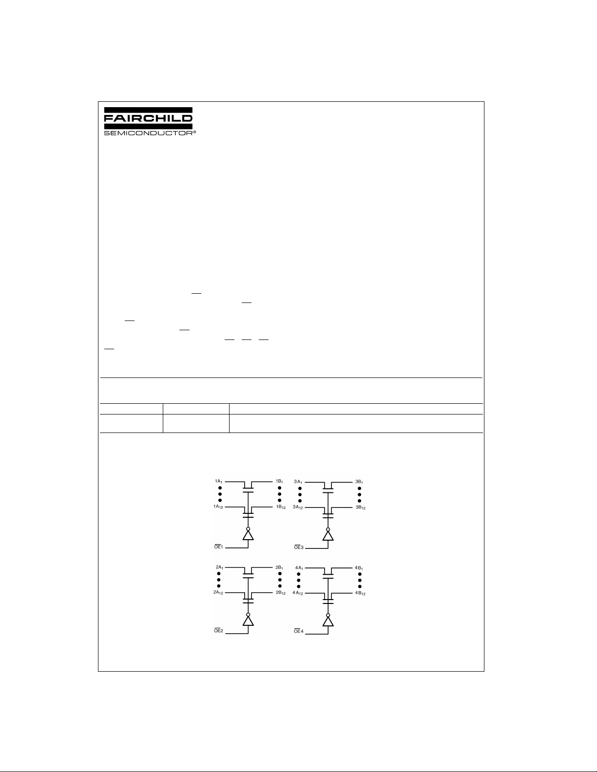
General Description
The Fairchild Switch FSTD32211 provides up to 48-bits of
high-speed CMOS TTL- compatible bu s switching. T he low
on resistance of the switch allows inputs to be connected to
outputs without adding propagation delay or generating
additional ground b ounce noise. A diode to V
integrated into the circuit to allow for leve l shifting b etween
5V inputs and 3.3V outputs.
The device can be organize d as four 12-bit, two 24-bit, or
one 48-bit bus swit ch. When routed as a 40-bi t bu s sw it ch,
the device can be orga nized as four 10-bit, two 20 -bit or
one 40-bit bus switch. When OE
and Port 1A is connected to Por t 1B. When OE
the switch is ON and Port 2A is connected to Port 2B.
When OE
nected to Port 3B. When OE
Port 4A is connected to Port 4B. When OE
OE
A and B Ports.
is LOW, the switch is ON and Port 3A is con-
3
are HIGH, a hig h im pe dan ce state exists betw ee n t he
4
is LOW, the switch is ON
1
is LOW, the switch is ON and
4
has been
CC
is LOW,
2
, OE2, OE3, or
1
Features
■ 4Ω switch connection between two ports
■ Voltage level shifting
■ Minimal propagation delay through the switch
■ Low l
CC
■ Zero bounce in flow-through mode
■ Control inputs compatible with TTL level
■ Packaged in plastic Fine-Pitch Ball Grid Array (FBGA)
Ordering Code:
Order Number Package Number Package Description
FSTD32211G
(Note 1)(Note 2)
Note 1: Ordering code “G” indicates Trays.
Note 2: Devices also available in Tape and Reel. Specify by appending th e s uffix let t er “X” to the ordering code.
BGA114A 114-Ball Fine-Pitch Ball Grid Array (FBGA), JEDEC MO-205, 5.5mm Wide
Logic Diagram
© 2002 Fairchild Semiconductor Corporation DS500378 www.fairchildsemi.com
Page 2
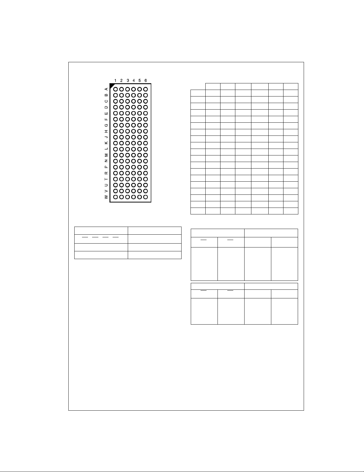
Connection Diagram
FSTD32211
(Top Thru View)
Pin Descriptions
Pin Name Description
OE
, OE2, OE3, OE
1
1A, 2A, 3A, 4A Bus A
1B, 2B, 3B, 4B Bus B
FBGA Pin Assignments
(40-Bit Routing)
123 4 56
A 1A
B 1A41A3GND OE11B31B
C 1A61A5GND GND 1B51B
D 1A81A7GND GND 1B71B
E 1A101A9V
F 2A22A1V
G 2A42A3V
H 2A62A5GND GND 2B52B
J 2A82A72A92B92B72B
K 2A103A10GND GND 3B102B
L 3A93A8GND GND 3B83B
M 3A73A6GND V
N 3A53A4V
P 3A33A2V
R 3A14A10GND GND 4B103B
T 4A94A8GND GND 4B84B
U 4A74A6GND 4B14B64B
V 4A54A44A1OE44B44B
W 4A34A2OE
1A1NC OE21B11B
2
CCVCC
CCVCC
GND 2B32B
CC
CC
CCVCC
CCVCC
NC 4B24B
3
1B91B
2B12B
3B63B
3B43B
3B23B
2
4
6
8
10
2
4
6
8
10
9
7
5
3
1
9
7
5
3
Truth Tables
Inputs Inputs/Outputs
Bus Switch Enables
4
OE
1
LL1A = 1B 2A = 2B
LH1A = 1B Z
HLZ2A
HHZZ
OE
3
LL3A
LH3A
HLZ4A
HHZZ
OE
2
1A, 1B 2A, 2B
Inputs Inputs/Outputs
OE
4
3A, 3B 4A, 4B
= 3B 4A = 4B
= 3B Z
= 2B
= 4B
www.fairchildsemi.com 2
Page 3
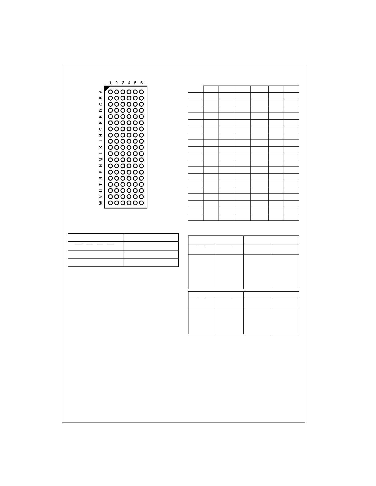
Connection Diagram
(Top Thru View)
Pin Descriptions
Pin Name Description
OE
, OE2, OE3, OE
1
1A, 2A, 3A, 4A Bus A
1B, 2B, 3B, 4B Bus B
4
Bus Switch Enables
FBGA Pin Assignments
(48-Bit Routing)
123 4 56
A 1A
1A1NC OE21B11B
2
B 1A41A31A7OE11B31B
C 1A61A5GND 1B71B51B
D 1A101A91A81B81B91B
E 1A121A112A12B11B111B
F 2A42A32A22B22B32B
G 2A62A5V
GND 2B52B
CC
H 2A82A7GND GND 2B72B
J 2A102A92A112B
11
2B92B
K 2A123A12GND GND 3B122B
L 3A113A10GND GND 3B103B
M 3A93A8GND V
CC
3B83B
N 3A73A63A23B23B63B
P 3A53A43A13B13B43B
R 3A34A124A84B84B123B
T 4A114A104A74B74B104B
U 4A94A6GND 4B14B64B
V 4A54A44A1OE44B44B
W 4A34A2OE3NC 4B24B
Truth Tables
Inputs Inputs/Outputs
OE
1
OE
2
LL1A
LH1A = 1B Z
HLZ2A
HHZZ
Inputs Inputs/Outputs
OE
3
OE
4
LL3A
LH3A
HLZ4A
HHZZ
1A, 1B 2A, 2B
= 1B 2A = 2B
3A, 3B 4A, 4B
= 3B 4A = 4B
= 3B Z
FSTD32211
2
4
6
10
12
4
6
8
10
12
11
9
7
5
3
11
9
5
3
= 2B
= 4B
3 www.fairchildsemi.com
Page 4

Absolute Maximum Ratings(Note 3) Recommended Operating
Supply Voltage (VCC) 0.5V to +7.0V
DC Switch Voltage (V
DC Input Control Pin Voltage (V
FSTD32211
DC Input Diode Current (l
DC Output (I
DC V
OUT
/GND Current (ICC/I
CC
Storage Temperature Range (T
) (Note 4) −0.5V to +7.0V
S
)(Note 5) −0.5V to +7.0V
IN
) V
< 0V −50 mA
IK
IN
) 128 mA
) +/− 100 mA
GND
) −65°C to +150 °C
STG
Conditions
Power Supply Operating (V
Input Voltage (V
Output Voltage (V
Input Rise and Fall Time (t
Switch Control Input 0 ns/V to 5 ns/V
Switch I/O 0 ns/V to DC
Free Air Operating Temperature (T
Note 3: The “Absolute Maximum Ratings” are those values bey ond which
the safety of the d evice cannot be guaranteed. The device sh ould not be
operated at these limit s. The parametric values defin ed in the Electrical
Characteristics tables are not guaranteed at the absolute maximum rating.
The “Recomme nded O peratin g Cond itions ” table will defin e the condition s
for actual device operation.
is the volt age observed / applied at either A or B Ports across t he
Note 4: V
S
switch.
Note 5: The input and output ne gative vo ltage ra tings may be excee ded if
the input and output diode current ratings are observed.
Note 6: Unused control inputs must be held HIGH or LOW. They may not
float.
(Note 6)
CC)
)0V to 5.5V
IN
)0V to 5.5V
OUT
, tf)
r
)-40 °C to +85 °C
A
DC Electrical Characteristics
V
Symbol Parameter
V
IK
V
IH
V
IL
V
OH
I
I
I
OZ
R
ON
I
CC
∆ I
CC
Note 7: Typi c al values are at VCC = 5.0V and TA= +25°C
Note 8: Measured by the volta ge drop between A an d B pins at the indicated c urrent through the switch. On Resistance is determined by the lower of the
voltages on the two (A or B) pins.
Clamp Diode Voltage 4.5 −1.2 V IIN = −18 mA
HIGH Level Input Voltage 4.5 - 5.5 2.0 V
LOW Level Input Voltage 4.5 - 5.5 0.8 V
HIGH Level 4.5 - 5.5 See Figure 3 V
Input Leakage Current 5.5 ±1.0 µA0 ≤ VIN ≤ 5.5V
OFF-STATE Leakage Current 5.5 ±1.0 µA0 ≤ A, B ≤ V
Switch On Resistance 4.5 4 7 Ω VIN = 0V, IIN = 64 mA
(Note 8) 4.5 4 7 Ω V
Quiescent Supply Current
Increase in I
per Input 5.5 2.5 mA One Input at 3.4V
CC
CC
(V)
010µAV
4.5 35 50 Ω VIN = 2.4V, IIN = 15 mA
5.5
TA = −40 °C to +85 °C
Min Typ
(Note 7)
Units Conditions
Max
1.5 mA
10 µA
= 5.5V
IN
CC
= 0V, IIN = 30 mA
IN
OE1 = OE2 = GND
= VCC or GND, I
V
IN
OE1 = OE2 = V
VIN = VCC or GND, I
Other Inputs at VCC or GND
4.5V to 5.5V
= 0
OUT
CC
= 0
OUT
www.fairchildsemi.com 4
Page 5

AC Electrical Characteristics
= −40 °C to +85 °C,
T
A
C
= 50pF, RU = RD = 500Ω
Symbol Parameter
L
= 4.5 – 5.5V
V
CC
Units Conditions
Figure
Number
Min Max
t
, t
PHL
t
PZH
t
PHZ
Note 9: This par ameter is guaranteed by design but is not test ed. The bus swit c h c ontributes no propagation delay other than t he RC delay of the typical On
Resistance of the sw it c h and the 50pF load capa citance, when drive n by an ideal voltage sourc e (zero output impe dance).
Propagation Delay Bus to Bus (Note 9) 0.25 ns VI = OPEN Figures
PLH
, t
Output Enable Time 1.5 10.0 ns VI = 7V for t
PZL
, t
Output Disable Time 1.5 9.0 ns VI = 7V for t
PLZ
V
VI = OPEN for t
PZL Figures
= OPEN for t
I
PZH
PLZ Figures
PHZ
Capacitance (Note 10)
Symbol Parameter Typ Max Units Conditions
C
IN
C
I/O
Note 10: TA = +25°C, f = 1 MHz, Capacitance is characterized but not tested.
Control Pin Input Capacitance 3 pF VCC = 5.0V
Input/Output Capacitance 6 pF VCC, OE = 5.0V
AC Loading and Waveforms
FSTD32211
1, 2
1, 2
1, 2
Note: Input driven by 50Ω source terminated in 50Ω
includes load and stray capacitance
Note: C
L
Note: Input PRR = 1.0 MHz, t
= 500 ns
W
FIGURE 1. AC Test Circuit
FIGURE 2. AC Waveforms
5 www.fairchildsemi.com
Page 6

Output Voltage HIGH vs. Supply Voltage
FSTD32211
FIGURE 3.
www.fairchildsemi.com 6
Page 7

Physical Dimensions inches (millimeters) unless otherwise noted
FSTD32211 40/48-Bit Bus Switch with Level Shifting
114-Ball Fine-Pitch Ball Grid Array (FBGA), JEDEC MO-205, 5.5mm Wide
Package Number BGA114A
Technology Description
The Fairchild Switch family derives from and embodies Fairchild’s proven switch t echnology used for several years in it s
74LVX3L384 (FST3384) bus switch product.
Fairchild does not assume any responsibility for use of any circuitry described , no circuit patent licenses are implied and
Fairchild reserves the right at any time without notice to change said circuitry and specifications.
LIFE SUPPORT POLICY
FAIRCHILD’S PRODUCTS ARE NOT AUTHORIZED FOR USE AS CRITICAL COMPONENTS IN LIFE SUPPORT
DEVICES OR SYSTEMS WITHOUT THE EXPRESS WRITTEN APPROVAL OF THE PRESIDENT OF FAIRCHILD
SEMICONDUCTOR CORPORATION. As used herein:
1. Life support devices or systems are dev ic es or syste ms
which, (a) are intended for surgical implant into the
body, or (b) support or sustain life, and (c) whose failure
to perform when properly used in accordance with
instructions for use provide d in the l abe ling, can be reasonably expected to result in a significant injury to the
user.
2. A critical compo nent in any com ponen t of a life s upp ort
device or system whose failure to perform can be reasonably expected to cause the failure of the life support
device or system, or to affect its safety or effectiveness.
www.fairchildsemi.com
7 www.fairchildsemi.com
 Loading...