

Page 1
FQA11N90C
www.DataSheet4U.com
900V N-Channel MOSFET
FQA11N90C 900V N-Channel MOSFET
September 2006
®
QFET
Features
• 11A, 900V, R
• Low gate charge ( typical 60 nC)
• Low Crss ( typical 23pF)
•Fast switching
• 100% avalanche tested
• Improved dv/dt capability
= 1.1Ω @VGS = 10 V
DS(on)
GSD
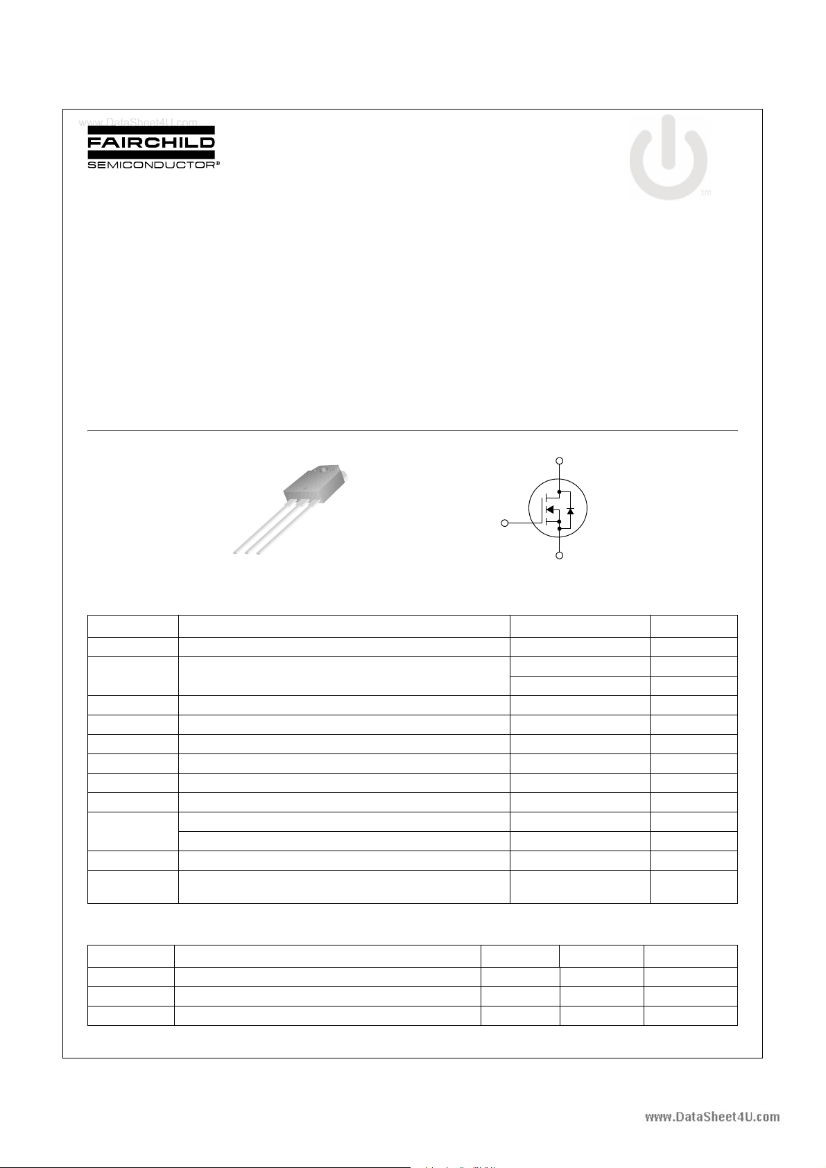
TO-3P
FQA Series
Description
These N-Channel enhancement mode power field effect
transistors are produced using Fairchild’s proprietary, planar
stripe, DMOS technology.
This advanced technology has been especially tailored to
minimize on-state resistance, provide superior switching
performance, and withstand high energy pulse in the avalanche
and commutation mode. These devices are well suited for high
efficient switched mode power supplies, active power factor
correction, electronic lamp ballast based on half bridge
topology.
D
G
S
Absolute Maximum Ratings
Symbol Parameter FQA11N90C Units
V
DSS
I
D
I
DM
V
GSS
E
AS
I
AR
E
AR
dv/dt Peak Diode Recovery dv/dt
P
D
, T
T
J
STG
T
L
Drain-Source Voltage 900 V
Drain Current - Continuous (TC = 25°C) 11.0 A
- Continuous (T
Drain Current - Pulsed
Gate-Source Voltage ± 30 V
Single Pulsed Avalanche Energy
Avalanche Current
Repetitive Avalanche Energy
Power Dissipation (TC = 25°C) 300 W
- Derate above 25°C 2.38 W/°C
Operating and Storage Temperature Range -55 to +150 °C
Maximum lead temperature for soldering purposes,
1/8" from case for 5 seconds
= 100°C) 6.9 A
C
(Note 1)
(Note 2)
(Note 1)
(Note 1)
(Note 3)
44.0 A
960 mJ
11. 0 A
30 mJ
4.0 V/ns
300 °C
Thermal Characteristics
Symbol Parameter Typ Max Units
R
θJC
R
θCS
R
θJA
©2006 Fairchild Semiconductor Corporation 1 www.fairchildsemi.com
FQA11N90C Rev. A1
Thermal Resistance, Junction-to-Case -- 0.42 °C/W
Thermal Resistance, Case-to-Sink 0.24 -- °C/W
Thermal Resistance, Junction-to-Ambient -- 40 °C/W
Page 2
Package Marking and Ordering Information
www.DataSheet4U.com
Device Marking Device Package Reel Size Tape Width Quantity
FQA11N90C FQA11N90C TO-3P -- -- 30
FQA11N90C FQA11N90C_F109 TO-3PN -- -- 30
FQA11N90C 900V N-Channel MOSFET
Electrical Characteristics T
= 25°C unless otherwise noted
C
Symbol Parameter Test Conditions Min Typ Max Units
Off Characteristics
BV
DSS
∆BV
DSS
∆T
J
I
DSS
I
GSSF
I
GSSR
On Characteristics
V
GS(th)
R
DS(on)
g
FS
Dynamic Characteristics
C
iss
C
oss
C
rss
Switching Characteristics
t
d(on)
t
r
t
d(off)
t
f
Q
g
Q
gs
Q
gd
Drain-Source Diode Characteristics and Maximum Ratings
I
S
I
SM
V
SD
t
rr
Q
rr
NOTES:
1. Repetitive Rating : Pulse width limited by maximum junction temperature
2. L = 15mH, IAS =11.0A, VDD = 50V, RG = 25 Ω, Starting TJ = 25°C
3. ISD ≤ 11.0A, di/dt ≤200A/µs, VDD ≤ BV
4. Pulse Test : Pulse width ≤ 300µs, Duty cycle ≤ 2%
5. Essentially independent of operating temperature
Drain-Source Breakdown Voltage VGS = 0 V, ID = 250 µA 900 -- -- V
/
Breakdown Voltage Temperature Coefficient ID = 250 µA, Referenced to 25°C -- 1.02 -- V/°C
Zero Gate Voltage Drain Current VDS = 900 V, VGS = 0 V -- -- 10 µA
= 720 V, TC = 125°C -- -- 100 µA
V
DS
Gate-Body Leakage Current, Forward VGS = 30 V, VDS = 0 V -- -- 100 nA
Gate-Body Leakage Current, Reverse VGS = -30 V, VDS = 0 V -- -- -100 nA
Gate Threshold Voltage VDS = VGS, ID = 250 µA3.0--5.0V
Static Drain-Source On-Resistance VGS = 10 V, ID = 5.5 A -- 1.12 1.4 Ω
Forward Transconductance VDS = 50 V, ID = 5.5 A (Note 4) -- 9.0 -- S
Input Capacitance VDS = 25 V, VGS = 0 V,
Output Capacitance -- 215 280 pF
Reverse Transfer Capacitance -- 23 30 pF
f = 1.0 MHz
Turn-O n Delay Time VDD = 450 V, ID = 11.0A,
R
= 25 Ω
Turn-O n Rise Time --
Turn-Off Delay Time --
G
(Note 4, 5)
Turn-Off Fall Time --
Total Gate Charge VDS = 720 V, ID = 11.0A,
V
= 10 V
Gate-Source Charge --
Gate-Drain Charge --
GS
(Note 4, 5)
-- 2530 3290 pF
--
--
60 130
130 270
130 270
85 180
60 80
13
25
-- nC
-- nC
ns
ns
ns
ns
nC
Maximum Continuous Drain-Source Diode Forward Current -- -- 11.0 A
Maximum Pulsed Drain-Source Diode Forward Current -- -- 44.0 A
Drain-Source Diode Forward Voltage VGS = 0 V, IS =11.0 A -- -- 1.4 V
Reverse Recovery Time VGS = 0 V, IS = 11.0 A,
dI
/ dt = 100 A/µs (Note 4)
Reverse Recovery Charge -- 17.0 --
Starting TJ = 25°C
DSS,
F
-- 1000 -- ns
µC
FQA11N90C Rev. A1
2 www.fairchildsemi.com
Page 3
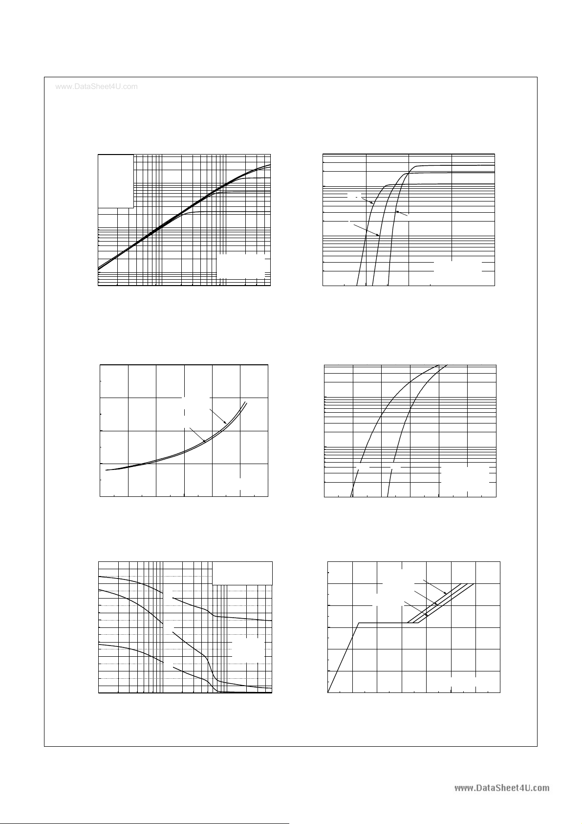
Typical Performance Characteristics
www.DataSheet4U.com
Figure 1. On-Region Characteristics Figure 2. Transfer Characteristics
V
GS
Top : 15.0 V
10.0 V
8.0 V
1
, Drain Current [A]
D
I
10
0
10
-1
10
10
7.0 V
6.5 V
6.0 V
Bottom : 5.5 V
-1
0
10
VDS, Drain-Source Voltage [ V]
Notes :※
1. 250µ s Pulse Test
= 25℃
2. T
C
1
10
1
10
150oC
25oC
0
10
, Drain Current [A]
D
I
-1
10
246810
VGS, Gate-Source Voltage [V]
Figure 3. On-Resistance Variation vs. Figure 4. Body Diode Forward Voltage
Drain Current and Gate Voltage Variation vs. Source Current
and Temperatue
-55oC
Notes :※
1. VDS = 50V
2. 250µ s Pulse Test
FQA11N90C 900V N-Channel MOSFET
2.5
2.0
[Ω ],
1.5
DS(ON)
R
1.0
VGS = 10V
VGS = 20V
Drain-Source On-Resistance
0.5
0 5 10 15 20 25 30
ID, Dr ain Cur rent [ A]
Note : T※J = 25℃
1
10
0
10
, Reverse Drain Current [A]
DR
I
-1
10
0.2 0.4 0.6 0.8 1.0 1.2 1.4
150℃
VSD, Source-Drain voltage [V]
25℃
Notes :※
1. VGS = 0V
2. 250µ s Pulse Test
Figure 5. Capacitance Characteristics Figure 6. Gate Charge Characteristics
4500
4000
3500
3000
2500
2000
1500
Capacitance [pF]
1000
500
0
-1
10
C
iss
C
oss
C
rss
0
10
C
= Cgs + Cgd (Cds = shorted)
iss
= Cds + C
C
oss
gd
C
= C
rss
gd
Notes :※
1. VGS = 0 V
2. f = 1 MHz
1
10
12
10
8
6
4
, Gate-Source Voltage [V]
2
GS
V
0
0 10203040506070
VDS, Drain-Source Vol tage [ V]
VDS = 180V
VDS = 450V
VDS = 720V
Note : I※D = 11A
QG, Total Gate Charge [nC]
FQA11N90C Rev. A1
3 www.fairchildsemi.com
Page 4

Typical Performance Characteristics (Continued)
www.DataSheet4U.com
Figure 7. Breakdown Voltage Variation Figure 8. On-Resistance Variation
vs. Temperature vs. Temperature
FQA11N90C 900V N-Channel MOSFET
1.2
3.0
2.5
1.1
2.0
1.0
, (Normalized)
DSS
BV
0.9
Note s :※
1. VGS = 0 V
2. I
Drain-Source Breakdown Voltage
0.8
-100 - 50 0 50 100 150 200
TJ, Juncti on Temperat ure [oC]
= 250 µ A
D
1.5
, (Normalized)
1.0
DS(ON)
R
Drain-Source On-Resistance
0.5
0.0
-100 -50 0 50 100 150 200
TJ, Junct ion Temperatur e [oC]
Figure 9. Maximum Safe Operating Area Figure 10. Maximum Drain Current
vs. Case Temperature
, Case Temperature [ ]℃
, Drain Current [A]
I
2
10
1
10
Operati on in This Are a
is Li mited by R
DS(on)
1 ms
100 µs
10 µs
12
10
8
10 ms
0
DC
10
D
-1
10
-2
10
0
10
Notes :※
1. TC = 25 oC
2. T
3. Single Pulse
1
10
= 150 oC
J
2
10
3
10
VDS, Drai n-Sour ce Volt age [ V]
6
4
, Drain Current [A]
D
I
2
0
25 50 75 100 125 150
T
C
Figure 11. Transient Thermal Response Curve
Notes :※
1. VGS = 10 V
= 5.5 A
2. I
D
FQA11N90C Rev. A1
D=0.5
-1
10
0.2
0.1
0.05
0.02
(t), Thermal Response
-2
0.01
10
θ JC
Z
-5
10
sin g le p u ls e
-4
10
-3
10
-2
10
Notes :※
1. Z
(t) = 0.4 2 /W M ax.℃
θ JC
2. D uty F a cto r, D =t1/t
3. TJM - TC = PDM * Z
P
DM
t
1
t
2
-1
10
10
2
(t)
θ JC
0
1
10
t1, Square W ave Pulse Duration [sec]
4 www.fairchildsemi.com
Page 5

Gate Charge Test Circuit & Waveform
www.DataSheet4U.com
Resistive Switching Test Circuit & Waveforms
FQA11N90C 900V N-Channel MOSFET
FQA11N90C Rev. A1
Unclamped Inductive Switching Test Circuit & Waveforms
5 www.fairchildsemi.com
Page 6

Peak Diode Recovery dv/dt Test Circuit & Waveforms
www.DataSheet4U.com
FQA11N90C 900V N-Channel MOSFET
FQA11N90C Rev. A1
6 www.fairchildsemi.com
Page 7

Mechanical Dimensions
www.DataSheet4U.com
ø3.20 ±0.10
15.60 ±0.20
13.60 ±0.20
9.60 ±0.20
TO-3P
3.80 ±0.20
4.80 ±0.20
+0.15
1.50
–0.05
FQA11N90C 900V N-Channel MOSFET
13.90 ±0.20
2.00 ±0.20
3.00 ±0.20
1.00 ±0.20
5.45TYP
±0.30]
[5.45
12.76 ±0.20
5.45TYP
±0.30]
[5.45
19.90 ±0.20
3.50 ±0.20
23.40 ±0.20
16.50 ±0.30
18.70 ±0.20
1.40 ±0.20
+0.15
0.60
–0.05
FQA11N90C Rev. A1
Dimensions in Millimeters
7 www.fairchildsemi.com
Page 8

Mechanical Dimensions (Continued)
www.DataSheet4U.com
FQA11N90C 900V N-Channel MOSFET
TO-3PN
FQA11N90C Rev. A1
Dimensions in Millimeters
8 www.fairchildsemi.com
Page 9

TRADEMARKS
www.DataSheet4U.com
The following are registered and unregistered trademarks Fairchild Semiconductor owns or is authorized to use and is not intended to be
an exhaustive list of all such trademarks.
ACEx™
ActiveArray™
Bottomless™
Build it Now™
CoolFET™
CROSSVOLT™
DOME™
EcoSPARK™
2
E
CMOS™
EnSigna™
FACT™
®
FAST
FASTr™
FPS™
FRFET™
FACT Quiet Series™
GlobalOptoisolator™
GTO™
HiSeC™
2
I
C™
i-Lo™
ImpliedDisconnect™
IntelliMAX™
ISOPLANAR™
LittleFET™
MICROCOUPLER™
MicroFET™
MicroPak™
MICROWIRE™
MSX™
MSXPro™
Across the board. Around the world.™
The Power Franchise
®
OCX™
OCXPro™
OPTOLOGIC
®
OPTOPLANAR™
PACMAN™
POP™
Power247™
PowerEdge™
PowerSaver™
PowerTrench
QFET
®
®
QS™
QT Optoelectronics™
Quiet Series™
RapidConfigure™
RapidConnect™
µSerDes™
ScalarPump™
SILENT SWITCHER
SMART START™
SPM™
Stealth™
SuperFET™
SuperSOT™-3
SuperSOT™-6
SuperSOT™-8
SyncFET™
TCM™
TinyBoost™
TinyBuck™
TinyPWM™
TinyPower™
TinyLogic
®
TINYOPTO™
TruTranslation™
UHC™
Programmable Active Droop™
DISCLAIMER
FAIRCHILD SEMICONDUCTOR RESERVES THE RIGHT TO MAKE CHANGES WITHOUT FURTHER NOTICE TO ANY PRODUCTS HEREIN TO
IMPROVE RELIABILITY, FUNCTION OR DESIGN. FAIRCHILD DOES NOT ASSUME ANY LIABILITY ARISING OUT OF THE APPLICATION OR USE OF
ANY PRODUCT OR CIRCUIT DESCRIBED HEREIN; NEITHER DOES IT CONVEY ANY LICENSE UNDER ITS PATENT RIGHTS, NOR THE RIGHTS OF
OTHERS. THESE SPECIFICATIONS DO NOT EXPAND THE TERMS OF FAIRCHILD’S WORLDWIDE TERMS AND CONDITIONS, SPECIFICALLY THE
WARRANTY THEREIN, WHICH COVERS THESE PRODUCTS.
®
UniFET™
UltraFET
VCX™
Wire™
®
FQA11N90C 900V N-Channel MOSFET
LIFE SUPPORT POLICY
FAIRCHILD’S PRODUCTS ARE NOT AUTHORIZED FOR USE AS CRITICAL COMPONENTS IN LIFE SUPPORT DEVICES OR SYSTEMS WITHOUT
THE EXPRESS WRITTEN APPROVAL OF FAIRCHILD SEMICONDUCTOR CORPORATION.
As used herein:
1. Life support devices or systems are devices or systems which,
(a) are intended for surgical implant into the body, or (b) support
or sustain life, or (c) whose failure to perform when properly used
in accordance with instructions for use provided in the labeling,
2. A critical component is any component of a life support device
or system whose failure to perform can be reasonably expected to
cause the failure of the life support device or system, or to affect
its safety or effectiveness.
can be reasonably expected to result in significant injury to the
user.
PRODUCT STATUS DEFINITIONS
Definition of Terms
Datasheet Identification Product Status Definition
Advance Information Formative or In
Design
This datasheet contains the design specifications for
product development. Specifications may change in
any manner without notice.
Preliminary First Production This datasheet contains preliminary data, and
supplementary data will be published at a later date.
Fairchild Semiconductor reserves the right to make
changes at any time without notice in order to improve
design.
No Identification Needed Full Production This datasheet contains final specifications. Fairchild
Semiconductor reserves the right to make changes at
any time without notice in order to improve design.
Obsolete Not In Production This datasheet contains specifications on a product
FQA11N90C Rev. A1
that has been discontinued by Fairchild semiconductor.
The datasheet is printed for reference information only.
Rev. I20
9 www.fairchildsemi.com
 Loading...