

Page 1
FPNH10
g
FPNH10
C
B
E
TO-92
NPN RF Transistor
This device is designed for use in low noise UHF/VHF amplifiers,
with collector currents in the 100 µA to 20 mA range in common
emitter or common base mode of operations, and in low frequency
drift, high output UHF oscillators. Sourced from Process 42.
Absolute Maximum Ratings* TA = 25°C unless otherwise noted
Symbol Parameter Value Units
V
CEO
V
CBO
V
EBO
I
C
TJ, T
st
*These ratings are limiting values above which the serviceability of any semiconductor device may be impaired.
NOTES:
1) These ratings are based on a maximum junction temperature of 150 degrees C.
2) These are steady state limits. The factory should be consulted on applications involving pulsed or low duty cycle operations.
Collector-Emitt er Vol t age 25 V
Collector-Base Voltage 30 V
Emitter-Base Voltage 3.0 V
Collector Current - Continuous 50 mA
Operating and Stora ge Junction Temperature Range -55 to +150
°
C
Thermal Characteristics TA = 25°C unless otherwise noted
Symbol Characteristic Max Units
FPNH10
P
D
R
θ
JC
R
θ
JA
*Device mounted on FR-4 PCB 1.6" X 1.6" X 0.06."
2000 Fairchild Semiconductor Corporation FPNH10 Rev. A
Total Device Dissipation
Derate above 25°C
350
2.8
Thermal Resistance, Junction to Case 125
Thermal Resistance, Junc tion to Ambient 357
mW
mW/°C
°
C/W
°
C/W
Page 2
(BR)
(BR)
(BR)
NPN RF Transistor
(continued)
Electrical Characteristics TA = 25°C unless otherwise noted
Symbol Parameter Test Conditions Min Max Units
OFF CHARACTERISTICS
V
CEO
V
CBO
V
EBO
I
CBO
I
EBO
ON CHARACTERISTICS
h
FE
V
sat
CE(
V
BE(on)
SMALL SIGNAL CHARACTERISTICS
f
T
C
cb
C
rb
rb’C
c
*Pulse Test: Pulse Width ≤ 300 µs, Duty Cycle ≤ 2.0%
Collector-Emitter Sustaining Voltage* IC = 1.0 mA, IB = 0 25 V
Collector-Base Breakdown Voltage
Emitter-Base Breakdown Voltage
I
= 100 µA, IE = 0
C
I
= 10 µA, IC = 0
E
30 V
3.0 V
Collector Cutoff Current VCB = 25 V, IE = 0 100 nA
Emitter Cutoff Current VEB = 2.0 V, I
= 0 100 nA
C
DC Current Gain IC = 4.0 mA, VCE = 10 V 60
Collector-Emitter Saturation Voltage IC = 4.0 mA, IB = 0.4 mA 0.5 V
)
Base-Emitter On Voltage IC = 4.0 mA, VCE = 10 V 0.95 V
Current Gain - Bandwidth Product IC = 4.0 mA , VCE = 10 V,
Collector-Base Capacitance VCB = 10 V, IE = 0, f = 1.0 MH z 0.720 pF
Common-Base Feedback
Capacitance
Collector Base Time Constant IC = 4.0 mA , VCB = 10 V,
f = 100 MHz
VCB = 10 V, IE = 0, f = 1.0 MH z 0.34 0.65 pF
f = 31.8 MHz
650 MHz
9.0 ps
FPNH10
Spice Model
NPN (Is=69.28E-18 Xti=3 Eg=1.11 Vaf=100 Bf=308.6 Ne=1.197 Ise=69.28E-18 Ikf=22.83m Xtb=1.5 Br=1.11
Nc=2 Isc=0 Ikr=0 Rc=4 Cjc=1.042p Mjc=.2468 Vjc=.75 Fc=.5 Cje=1.52p Mje=.3223 Vje=.75 Tr=1.558n
Tf=135.8p Itf=.27 Vtf=10 Xtf=30 Rb=10)
Page 3
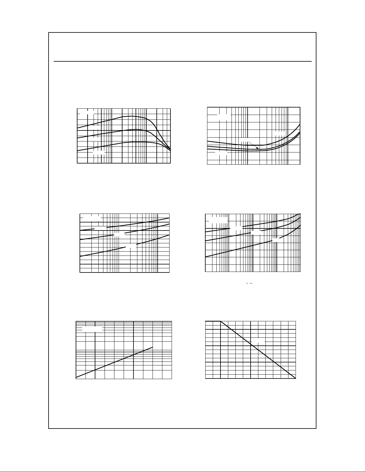
Typical Characteristics
C
FPNH10
NPN RF Transistor
(continued)
Typical Pulsed Current Gain
vs Collector Current
100
Vce = 5V
80
60
40
20
FE
h - TYPICAL PULSED CURRENT GAIN
125 °C
25 °C
- 40 °C
0
0.1 0.2 0.5 1 2 5 10 20 50
I - COLLECTOR CURRENT (mA)
C
Base-Emitter Saturation
Voltage vs Collector Current
1
β
= 10
0.9
0.8
0.7
0.6
0.5
0.4
0.3
BESAT
V - BASE-EMITTER VOLTAGE (V)
0.1 1 10 20
- 40 °C
25 °C
125 °C
I - COLLECTOR CURRENT (mA)
C
Collector-Emitter Saturation
Voltage vs Collector Current
0.2
β
= 10
125 °C
25 °C
- 40 °C
0.1 1 10 20
I - COLLECTOR CURRENT (mA)
- COLLECTOR-EMITTER VOLTAGE (V)
0.15
0.1
0.05
CESAT
Base-Emitter ON Voltage vs
Collector Current
1
V = 5V
CE
0.8
0.6
0.4
0.2
0.01 0.1 1 10 100
BE(ON)
V - BASE-EMITTER ON VOLTAGE (V)
- 40 °C
I - COLLECTOR CURRE N T (mA)
C
25 °C
125 °C
Collector-Cutoff Current
vs Ambient Temperature
10
V = 30V
CB
1
CBO
0.1
I - COLLECTOR CURRENT (nA)
25 50 75 100 125 150
T - AMBIENT TEMPERATURE ( C)
A
°
350
300
250
200
150
100
50
D
P - PO W E R DI SS IPATI O N (W )
0
0 25 50 75 100 125 150
Pow e r Dissipation
vs. Ambi ent Tem pe rature
TO-92
T - TE MP E RATUR E ( C)
A
o
Page 4

Common Base Y Parameters vs. Frequency
FPNH10
NPN RF Transistor
(continued)
Input Admittance
120
80
40
V = 10V
CE
I = 5 mA
C
0
-40
b
-80
ib
Y - INPUT ADMITTANCE (mmhos)
-120
100 200 500 1000
ib
f - FREQUENCY (MHz)
g
ib
Forward Transfer Admittance
120
b
80
40
0
-40
-80
fb
-120
Y - FORWARD ADMITTANCE (mmhos)
100 200 500 1000
fb
g
fb
f - FREQUENCY (MH z)
V = 10V
CE
I = 5 mA
C
Output Admittance
12
V = 10V
CE
10
I = 5 mA
C
8
6
4
2
ob
0
Y - OUTPUT ADMITTANCE (mmhos)
100 200 500 1000
f - FREQUENCY (MHz)
b
ob
g
ob
Reverse Transfer Admittance
8
V = 10V
CE
I = 5 mA
C
6
4
-b
rb
2
-g
rb
0
Y - REVERSE ADMITTANCE (mmhos)
100 200 500 1000
f - FREQUENCY (MHz)
rb
Page 5

Common Emitter Y Parameters vs. Frequency
FPNH10
NPN RF Transistor
(continued)
Input Admittance
24
V = 10V
CE
20
I = 2 mA
C
16
12
8
4
ie
Y - INPUT A DMITT ANCE (mmhos)
0
100 200 500 1000
f - FREQUENCY (MHz)
g
ie
b
ie
Forward Transfer Admittance
60
40
20
-20
g
fe
0
V = 10V
CE
I = 2 mA
C
Output Admittance
6
V = 10V
CE
5
I = 2 mA
C
4
b
3
2
1
oe
0
Y - OUTPUT ADMITTANCE (mmhos)
100 200 500 1000
f - FREQUENCY (MHz)
oe
g
oe
Reverse Transfer Admittance
1.2
V = 10V
CE
1
I = 2 mA
C
0.8
0.6
0.4
-b
re
-40
fe
-60
Y - FORWARD ADMITTANCE (mmhos)
100 200 500 1000
b
fe
f - FREQUENCY (MHz)
0.2
0
re
Y - REVERSE ADMITTA NCE (mmhos)
100 200 500 1000
-g
re
f - FREQUENCY (MHz)
Page 6

Test Circuits
FPNH10
NPN RF Transistor
(continued)
Input
50
ΩΩ
2.0 K
Ω 10 K
ΩΩ
1000 pF
T1
1000 pF
ΩΩ
Ω
ΩΩ
V
L1
1000 pF
BB
5.0-18 pF
0.8-10 pF
2.0 pF
ΩΩ
Ω
ΩΩ
L2
TUM
1000 pF
680
ΩΩ
Ω
ΩΩ
V
1000 pF
100 pF
0.8-10 pF
CC
FIGURE 1: Neutralized 200 MHz pF and NF Circuit
= 12 V
L1 - L3 turns No. 16 wire, 1/2 inch L x 1/4 inch ID
tapped 1 1/2 turns from cold side
L2 - L6 turns No. 14 wire, 1 inch L x 1/4 inch ID
tapped 1 1/2 turns from cold side
T1 - Pri. 1 turn No. 16 wire
Sec. 1 turn No. 18 wire
50 pF
(NOTE 2)
RFC
1000 pF
ΩΩ
2.2 K
Ω
ΩΩ
- V
ee
(NOTE 1)
RFC
V
CC
175 pF
1000 pF
500 mHz Output
ΩΩ
into 50
Ω
ΩΩ
NOTE 1: 2 turns No. 16 AWG wire, 3/8 inch OD, 1 1/4 inch long
NOTE 2: 9 turns No. 22 AWG wire, 3/16 inch OD, 1/2 inch long
FIGURE 2: 500 MHz Oscillator Circuit
Page 7

TRADEMARKS
The following are registered and unregistered trademarks Fairchild Semiconductor owns or is authorized to use and is
not intended to be an exhaustive list of all such trademarks.
ACEx™
Bottomless™
CoolFET™
CROSSVOLT™
DOME™
E2CMOS
EnSigna
TM
TM
FACT™
FACT Quiet Series™
FAST
FASTr™
GlobalOptoisolator™
GTO™
HiSeC™
ISOPLANAR™
MICROWIRE™
OPTOLOGIC™
OPTOPLANAR™
P ACMAN™
POP™
PowerTrench
QFET™
QS™
QT Optoelectronics™
Quiet Series™
SILENT SWITCHER
SMART ST ART™
SuperSOT™-3
SuperSOT™-6
SuperSOT™-8
SyncFET™
TinyLogic™
UHC™
VCX™
DISCLAIMER
FAIRCHILD SEMICONDUCTOR RESERVES THE RIGHT TO MAKE CHANGES WITHOUT FURTHER
NOTICE TO ANY PRODUCTS HEREIN T O IMPROVE RELIABILITY , FUNCTION OR DESIGN. FAIRCHILD
DOES NOT ASSUME ANY LIABILITY ARISING OUT OF THE APPLICA TION OR USE OF ANY PRODUCT
OR CIRCUIT DESCRIBED HEREIN; NEITHER DOES IT CONVEY ANY LICENSE UNDER ITS PA TENT
RIGHTS, NOR THE RIGHTS OF OTHERS.
LIFE SUPPORT POLICY
FAIRCHILD’S PRODUCTS ARE NOT AUTHORIZED FOR USE AS CRITICAL COMPONENTS IN LIFE SUPPORT
DEVICES OR SYSTEMS WITHOUT THE EXPRESS WRITTEN APPROVAL OF FAIRCHILD SEMICONDUCTOR CORPORA TION.
As used herein:
1. Life support devices or systems are devices or
systems which, (a) are intended for surgical implant into
the body, or (b) support or sustain life, or (c) whose
failure to perform when properly used in accordance
with instructions for use provided in the labeling, can be
reasonably expected to result in significant injury to the
user.
2. A critical component is any component of a life
support device or system whose failure to perform can
be reasonably expected to cause the failure of the life
support device or system, or to affect its safety or
effectiveness.
PRODUCT STA TUS DEFINITIONS
Definition of Terms
Datasheet Identification Product Status Definition
Advance Information
Preliminary
No Identification Needed
Obsolete
Formative or
In Design
First Production
Full Production
Not In Production
This datasheet contains the design specifications for
product development. Specifications may change in
any manner without notice.
This datasheet contains preliminary data, and
supplementary data will be published at a later date.
Fairchild Semiconductor reserves the right to make
changes at any time without notice in order to improve
design.
This datasheet contains final specifications. Fairchild
Semiconductor reserves the right to make changes at
any time without notice in order to improve design.
This datasheet contains specifications on a product
that has been discontinued by Fairchild semiconductor.
The datasheet is printed for reference information only.
Rev. G
 Loading...