

Page 1
February 2006
FPF2500-FPF2506
IntelliMAX™ Advanced Load Management Products
FPF2500-FPF2506 IntelliMAX™ Advanced Load Management Products
Features
4.5 to 20V Input Voltage Range
Controlled Turn-On
0.4A, 0.8A and Adjustable Current Limit Option
Undervoltage Lockout
Thermal Shutdown
<10uA Shutdown Current
Auto Restart
Fault Blanking
Applications
PDAs
Motor Drivers
Cell Phones
Digital Cameras
General Description
The FPF2500 through FPF2506 is a family of load switches
which provide full protection to systems and loads which may
encounter large current conditions. These devices contain a
0.23Ω current-limited N-channel MOSFET which can operate
over an input voltage range of 4.5-20V. Switch control is by a
logic input (ON) capable of interfacing directly with low voltage
control signals. Each part contains thermal shutdown protection
which shuts off the switch to prevent damage to the part when a
continuous over-current condition causes excessive heating.
When the switch current reaches the current limit, the part
operates in a constant-current mode to prohibit excessive
currents from causing damage. For the FPF2500, FPF2501,
FPF2503 and FPF2505, if the constant current condition still
persists after 5ms, these parts will shut off the switch and, for
the FPF2503 and FPF2505, the fault signal pin (FLAGB) will be
pulled low. The FPF2500, FPF2503, and FPF2505, have an
auto-restart feature which will turn the switch on again after
640ms if the ON pin is still active. The FPF2501 does not have
this auto-restart feature so the switch will remain off until the ON
pin is cycled. For the FPF2502, FPF2504 and FPF2506, a
current limit condition will immediately pull the fault signal pin
low and the part will remain in the constant-current mode until
the switch current falls below the current limit. For the FPF2500
through FPF2502, the minimum current limit is adjustable from
500mA to 2A. For the FPF2503 and FPF2504 the minimum
current is internally fixed at 400mA while that for the FPF2505
and FPF2506 is internally fixed at 800mA.
These parts are available in a space-saving 5 pin SOT23
package.
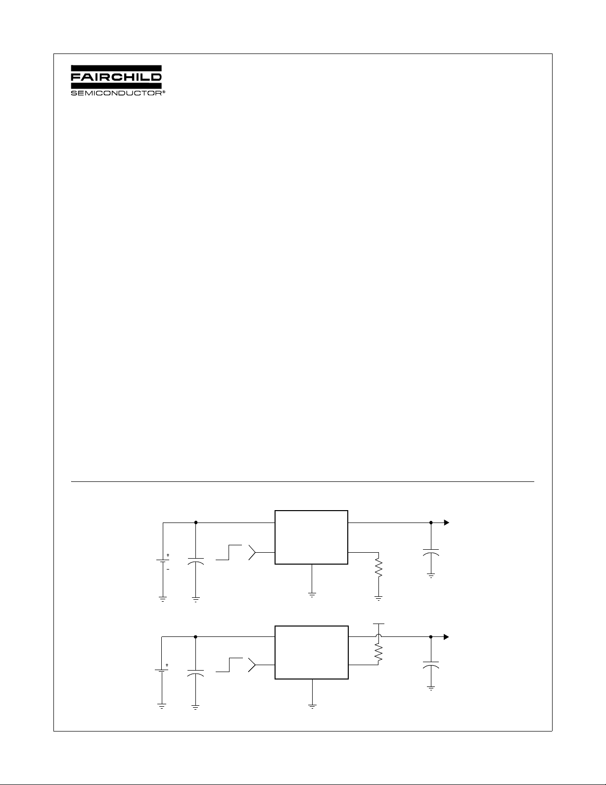
Typical Application Circuit
TO LOAD
TO LOAD
GND
GND
V
OUT
ISET
V
OUT
FLAGB
5.5V max
V
IN
FPF2500-FPF2502
OFF ON ON
5.5V max
V
IN
FPF2503- FPF2506
-
©2006 Fairchild Semiconductor Corporation 1 www.fairchildsemi.com
FPF2500-FPF2506 Rev. C4
OFF ON
5.5V max
ON
Page 2
Functional Block Diagram
V
IN
UVLO
FPF2500-FPF2506 IntelliMAX™ Advanced Load Management Products
ON
V
ON
IN
THERMAL
SHUTDOWN
UVLO
THERMAL
SHUTDOWN
CONTROL
LOGIC
CURRENT
LIMIT
FPF2500, FPF2501, FPF2502
CONTROL
LOGIC
CURRENT
LIMIT
V
OUT
I
SET
GND
V
OUT
FLAGB
Pin Configuration
FPF2500-FPF2506 Rev. C4
FPF2503, FPF2504
FPF2505, FPF2506
V
1
OUT
2
GND
FLAGB/ISET
34
SOT23-5
GND
V
5
IN
ON
2 www.fairchildsemi.com
Page 3
Pin Description
Pin Name Function
1 V
IN
2 GND Ground
3 ON ON Control Input:
4 FLAGB Fault Output (FPF2503-FPF2506): Active LO, open drain output which indicates on over
ISET Adjustable Current Limit Setting Resistor (FPF2500-FPF2502): An external resistor
5 V
OUT
Supply Input: Input to the power switch and the supply voltage for the IC
current supply under voltage or over temperature state.
connected between this pin and ground sets the current limit value.
Switch Output: Output of the power switch
Absolute Maximum Ratings
Parameter Min. Max. Unit
VIN, V
ON, FLAGB, ISET to GND -0.3 5.5 V
Power Dissipation @ T
Operating Temperature Range -40 125 °C
Storage Temperature -65 150 °C
Thermal Resistance, Junction to Ambient 150 °C/W
Electrostatic Discharge Protection HBM 2000 V
, to GND -0.3 20 V
OUT
=25°C (Note 1) 667 mW
A
MM 200 V
FPF2500-FPF2506 IntelliMAX™ Advanced Load Management Products
Recommended Operating Range
Parameter Min. Max. Unit
V
IN
Ambient Operating Temperature, T
A
4.5 20 V
-40 85 °C
Electrical Characteristics
VIN = 4.5 to 20V, TA = -40 to +85°C unless otherwise noted. Typical values are at VIN = 12V and TA = 25°C.
Parameter Symbol Conditions Min. Typ. Max Units
Basic Operation
Operating Voltage V
Quiescent Current I
Shutdown Current I
Latch-Off Current (Note 2) I
On-Resistance R
ON Input Logic High Voltage V
ON Input Logic Low Voltage V
IN
Q
SHDN
LATCHOFF
ON
IH
IL
ON Input Leakage V
Off Switch Leakage I
SWOFF
FLAGB Output Logic Low Voltage V
FLAGB Output High Leakage Current V
I
= 0mA, VIN = 12V, Von=5V 60 100 µA
OUT
FPF2501 45 µA
TA = 25°C, I
= -40 to +85°C, I
T
A
= 50mA 230 320 mΩ
OUT
= 50mA 300
OUT
VIN = 4.5V to 20V 0.9 V
VIN = 4.5V to 20V 0.4 V
= 5V or GND -1 1 µA
ON
VON = 0V, V
= 5V, I
IN
= 5V, Switch on 1 µA
IN
= 0V 0.01 µA
OUT
= 10mA 0.1 0.2 V
SINK
4.5 20 V
1 µA
FPF2500-FPF2506 Rev. C4
3 www.fairchildsemi.com
Page 4
Electrical Characteristics Cont.
VIN = 4.5 to 20V, TA = -40 to +85°C unless otherwise noted. Typical values are at VIN = 12V and TA = 25°C.
Parameter Symbol Conditions Min. Typ. Max Units
Protections
Current Limit I
LIM
TA=25 °C
Thermal Shutdown TJ Increasing 140 °C
Decreasing 130 °C
T
J
Under Voltage Shutdown UVLO V
Increasing 3.75 3.85 4.00 V
IN
Under Voltage Shutdown Hysteresis 100 mV
Dynamic
Turn on time t
Turn off time t
Rise Time t
V
OUT
Fall Time t
V
OUT
Over Current Blanking Time t
Auto-Restart Time t
ON
OFF
R
F
BLANK
RESTART
Short Circuit Response Time V
RL=500Ω, CL=1uF 1 ms
RL=500Ω, CL=1uF 0.1 ms
RL=500Ω, CL=1uF 3 ms
RL=500Ω, CL=1uF 1.5 ms
FPF2500, FPF2501, FPF2503, FPF2505
FPF2500, FPF2503, FPF2505 320 640 1280 ms
= 12V , VON = 5V
IN
Moderate Overcurrent Condition
FPF2503
FPF2504
FPF2505
FPF2506
FPF2500
FPF2501
FPF2502
400 600 800 mA
800 1200 1600
0.7xI
NOM
1.0xI
NOM
1.3xI
NOM
2.5 5 10 ms
3 µs
FPF2500-FPF2506 IntelliMAX™ Advanced Load Management Products
Note 1: Package power dissipation on 1square inch pad, 2 oz copper board.
Note 2: Applicable only to FPF2501. Latchoff current does not include current flowing into FLAGB.
FPF2500-FPF2506 Rev. C4
4 www.fairchildsemi.com
Page 5

Typical Characteristics
0
5
5
FPF2500-FPF2506 IntelliMAX™ Advanced Load Management Products
80
VON = V
75
70
65
60
SUPPLY CURRENT (uA)
55
50
4 6 8 10121416182
IN
SUPPLY VOLTAGE ( V)
80
75
70
65
60
55
50
SUPPLY CURRENT (uA)
45
40
-40 - 15 10 35 60 85
T
, JUNCTI ON TEMPERATURE (oC)
J
V
= 20V
V
= 12V
V
= 4.5V
Figure 1. Quiescent Current vs. Input Voltage Figure 2. Quiescent Current vs. Temperature
8.0
I_SHDN
7.5
7.0
6.5
6.0
5.5
5.0
SUPPLY CURRENT (uA)
4.5
4.0
-40 -15 10 35 60 8
Figure 3. I
VIN = 20V
VIN = 12V
TJ, JUNCTI ON TEMPERATURE (oC)
SHUTDOWN
Current vs. Temperature Figure 4. I
0.036
I_SWOFF
0.032
0.028
0.024
SUPPLY CURRENT (uA)
0.02
0.016
-40 -15 10 35 60 85
, JUNCTION TEMPERATURE (oC)
T
J
SWITCH-OFF
VIN = 20V
VIN = 12V
Current vs. Temperature
0.80
0.75
0.70
0.65
0.60
ON THRESHOL D (V)
0.55
0.50
4 6 8 101214161820
Figure 5. V
FPF2500-FPF2506 Rev. C4
, Input Voltage (V)
V
IN
IH
320
VIN = 12V
300
280
260
240
(mOhms)
ON
220
R
200
180
160
-40 -15 10 35 60 8
TJ, JUNCTI ON TEMPERATURE (oC)
vs. VIN Figure 6. R
5 www.fairchildsemi.com
vs. Temperature
(ON)
Page 6

Typical Characteristics
6
4
4
5
FPF2500-FPF2506 IntelliMAX™ Advanced Load Management Products
1400
R
= 20kΩ
1200
SET
1000
800
FPF2500, 2501, 2502
600
400
OUTPUT CURRENT (mA)
200
0
0123456789101112
V
- V
(V)
IN
OUT
1400
1200
FPF2505, 250
1000
800
600
FPF2503, 250
400
OUTPUT CURRENT ( mA)
200
0
0123456789101112
V
- V
(V)
IN
OUT
Figure 7. Current Limit vs. Output Voltage Figure 8. Current Limit vs. Output Voltage
1400
FPF2500, 2501, 2502
1300
1200
1100
1000
900
800
OUTPUT CURRENT (mA)
700
600
-40 - 15 10 35 60 85
, JUNCTION TEMPERATURE (oC)
T
J
1600
1400
1200
FPF2505, 2506
1000
800
600
400
OUTPUT CURRENT (mA)
FPF2503, 250
200
0
-40 -15 10 35 60 85
T
, JUNCT ION TEMPERATURE (oC)
J
Figure 9. Current Limit vs. Temperature Figure 10. Current Limit vs. Temperature
10
1
0.1
DELAY TIMES ( mS)
0.01
-40 - 15 10 35 60 8
FPF2500-FPF2506 Rev. C4
I
= 10mA
LOAD
V
= 12V
CC
TJ, JUNCT ION TEMPERATURE (oC)
Figure 11. T
10
I
LOAD
V
CC
TD
(ON)
TD
(OFF)
TURN-ON/OFF TIMES ( mS)
1
-40 -15 10 35 60 85
vs. Temperature Figure 12. T
ON/TOff
6 www.fairchildsemi.com
= 10mA
= 12V
T
(RISE)
T
(FALL)
, JUNCT ION TEMPERATURE (oC)
T
J
RISE/TFALL
vs. Temperature
Page 7

Typical Characteristics
5
FPF2500-FPF2506 IntelliMAX™ Advanced Load Management Products
7
6
5
4
FLAG-BLANKING TIME (mS)
3
-40 -15 10 35 60 8
TJ, JUNCT ION TEMPERATURE (oC)
Figure 13. T
vs. Temperature Figure 14. T
BLANK
VIN = 12V
V
DRV3
5V/DIV
V
OUT
10V/DIV
I
OUT
1A/DIV
FLAGB
5V/DIV
800
700
600
RESTART TIME (mS)
500
-40 -15 10 35 60 85
, JUNCTION TEMPERATURE (oC)
T
J
vs. Temperature
RESTART
V
= 12V
V
DRV3
5V/DIV
V
OUT
10V/DIV
IN
I
OUT
1A/DIV
FLAGB
5V/DIV
T
RESTART
5ms/DIV
Figure 15. T
(Switch is turned on to an overcurrent condition)
V
ON
5V/DIV
I
OUT
Response Figure 16. T
BLANK
10mA/DIV
VIN=12V, CIN=10uF
R
=500Ω, CL=1uF
L
2ms/DIV 2us/DIV
Figure 17. T
FPF2500-FPF2506 Rev. C4
Response Figure 18. T
ON
100ms/DIV
Response (FPF2505)
RESTART
V
ON
5V/DIV
I
OUT
10mAV/DIV
=12V, CIN=10uF
V
IN
=500Ω, CL=1uF
R
L
Response
OFF
7 www.fairchildsemi.com
Page 8

Typical Characteristics
FPF2500-FPF2506 IntelliMAX™ Advanced Load Management Products
V
10V/DIV
IN
I
OUT
10A/DIV
V
OUT
10V/DIV
C
=1uF, CIN=10uF
OUT
=500Ω, VON=5V
R
L
20us/DIV
V
10V/DIV
V
IN
ON
5V/DIV
I
OUT
1A/DIV
1ms/DIV
Figure 19. Short Circuit Response Figure 20. Current Limit Response
(Output is shorted to GND) (Output has a 4.7Ω, load)
Note 3: VDRV signal forces the device to go into overcurrent condition.
FPF2500-FPF2506 Rev. C4
8 www.fairchildsemi.com
Page 9

FPF2500-FPF2506 IntelliMAX™ Advanced Load Management Products
Description of Operation
The FPF2500 - FPF2506 are current limited switches that
protect systems and loads which can be damaged or disrupted
by the application of high currents. The core of each device is
a 0.23Ω P - channel MOSFET and a controller capable
of functioning over a wide input operating range of 4.5 V -20 V.
The controller protects against system malfunctions through
current limiting under-voltage lockout and thermal shutdown.
The current limit for FPF2500, FPF2501 and FPF2502 is
adjustable from 500 mA to 2 A through the selection of an
external resistor . The FPF2503 and FPF2504 the minimum
current is internally fixed at 400 mA while that for the
FPF2505 and FPF2506 is internally fixed at 800mA.
On/Off Control
The ON pin controls the state of the switch. When ON is high,
the switch is in the on state. Activating ON continuously holds
the switch in the on state so long as there is no fault. For all
versions, an under-voltage on V
excess of 140°C overrides the ON control to turn off the switch.
In addition, excessive currents will cause the switch to turn off in
the FPF2500, FPF2501, FPF2503 and FPF2505. The
FPF2500, FPF2503 and FPF2505 have an Auto-Restart feature
which will automatically turn the switch on again after 640ms.
For the FPF2501, the ON pin must be toggled to turn-on the
switch again. The FPF2502, FPF2504 and FPF2506 does not
turn off in response to an over current condition but instead
remains operating in a constant current mode so long as ON is
active and the thermal shutdown or under-voltage lockout have
not activated.
or a junction temperature in
IN
Current Limiting
The current limit ensures that the current through the switch
doesn't exceed a maximum value while not limiting at less than
a minimum value. For the FPF2500, FPF2501 and FPF2502,
the current at which the parts will limit is adjustable through the
selection of an external resistor connected to I
for selecting the resistor is found in the Application Info section.
For the FPF2503 and FPF2504 the minimum current is 400mA
and the maximum current is 800mA and for the FPF2505FPF2506 the minimum current is 800mA and the maximum
current is 1600mA. The FPF2500, FPF2501, FPF2503 and
FPF2505 have a blanking time of 5ms, nominally, during which
the switch will act as a constant current source. At the end of
the blanking time, the switch will be turned-off. For FPF2503
and FPF2505, at the end of the blanking time, the switch will be
turned-off and the FLAGB pin will activate to indicate that
current limiting has occurred. The FPF2502, FPF2504 and
FPF2506 have no current limit blanking period so they will
remain in a constant current state. For FPF2504 and FPF2506,
immediately upon a current limit condition FLAGB is activated.
The FPF2502, FPF2504 and FPF2506 devices will remain in
constant current state until the ON pin is cycled or the thermal
shutdown turns-off the switch.
. Information
SET
Under-Voltage Lockout
The under-voltage lockout turns-off the switch if the input
voltage drops below the under-voltage lockout threshold. With
the ON pin active, the input voltage rising above the undervoltage lockout threshold will cause a controlled turn-on of the
switch which limits current over-shoots.
Thermal Shutdown
The thermal shutdown protects the die from internally or
externally generated excessive temperatures. During an
over-temperature condition the switch is turned-off. The switch
automatically turns-on again if the temperature of the die drops
below the threshold temperature.
Ordering Information
Part Current Limit [A]
FPF2500 Adjustable (0.5-2.0 +/-30%) 2.5/5/10 320/640/1280 No
FPF2501 Adjustable (0.5-2.0 +/-30%) 2.5/5/10 NA No
FPF2502 Adjustable (0.5-2.0 +/-30%) 0 NA No
FPF2503 0.4/0.6/0.8 2.5/5/10 320/640/1280 Yes
FPF2504 0.4/0.6/0.8 0 NA Yes
FPF2505 0.8/1.2/1.6 2.5/5/10 320/640/1280 Yes
FPF2506 0.8/1.2/1.6 0 NA Yes
FPF2500-FPF2506 Rev. C4
Current Limit
Blanking Time
[ms]
9 www.fairchildsemi.com
Auto-Restart
Tim e
[ms] Fault Pin
Page 10

Application Information
Typical Application
FPF2500-FPF2506 IntelliMAX™ Advanced Load Management Products
V
IN
FPF2500-FPF2502
Battery
12V
OFF ON ON
C1=10uF
5.5V max
V
IN
FPF2503-FPF2506
Battery
12V
-
OFF ON ON
5.5V max
C1=10uF
Setting Current Limit
The FPF2500, FPF2501, and FPF2502 have a current limit
which is set with an external resistor connected between I
and GND. This resistor is selected by using the following
SET
equation,
R
R
12500 I
SET
is in Ohms and I
SET
× e
×=
SET
is in Amps
SET
The following table can also be used to select R
SET
SET
(1)
. A typical
0.485 I
×()
application would be the 0.500A current that is required by a
single USB port. Using the table below an appropriate selection
for the R
resistor would be 12.4KΩ. This will ensure that the
SET
port load could draw 0.525A, but not more than 0.875A.
Likewise for a dual port system, an R
always deliver at least 1.050A and never more than 1.750A.
of 34.8KΩ would
SET
Input Capacitor
To limit the voltage drop on the input supply caused by transient
in-rush currents when the switch turns-on into a discharged load
capacitor or a short-circuit, a capacitor needs to be placed
between V
close to the pins is usually sufficient. Higher values of C
be used to further reduce the voltage drop.
and GND. A 0.1uF ceramic capacitor, CIN, placed
IN
IN
can
V
OUT
ISET
GND
C2=1uF
RSET
5.5V max
V
OUT
R1=100K
Ω
FLAGB
GND
Current Limit Various R
R
SET
[KΩ]
Min. Current
Limit
[A]
C2=1uF
Values
SET
Typ. Current
Limit
[A]
7.87 0.375 0.500 0.625
10.0 0.450 0.600 0.750
12.4 0.525 0.700 0.875
14.7 0.600 0.800 1.000
17.4 0.675 0.900 1.125
20.5 0.750 1.000 1.250
23.2 0.825 1.100 1.375
26.7 0.900 1.200 1.500
30.9 0.975 1.300 1.625
34.8 1.050 1.400 1.750
39.0 1.125 1.500 1.875
43.2 1.200 1.600 2.000
48.7 1.275 1.700 2.125
53.6 1.350 1.800 2.250
29.0 1.425 1.900 2.375
64.9 1.500 2.000 2.500
R2=240Ω
R2=240
Max. Current
Limit
[A]
Ω
FPF2500-FPF2506 Rev. C4
10 www.fairchildsemi.com
Page 11

FPF2500-FPF2506 IntelliMAX™ Advanced Load Management Products
Output Capacitor
A 0.1uF capacitor C
GND. This capacitor will prevent parasitic board inductances
from forcing V
the FPF2501, FPF2503 and FPF2505, the total output
capacitance needs to be kept below a maximum value,
C
OUT(max)
condition and turning off the switch. The maximum output
capacitance can be determined from the following formula,
OUT
, to prevent the part from registering an over-current
max()
C
OUT
should be placed between V
OUT,
below GND when the switch turns-off. For
I
------------------------------------------------------------------=
LIM
min()t
V
IN
BLANK
min()×
OUT
and
(2)
Power Dissipation
Due to the wide input voltage range that the parts can accept
and the high currents at which the current limit can be set, care
must be taken to prevent excessive power dissipation in the part
from interrupting the switching of power to a load. During
normal operation as a switch, the power dissipated in the part
will depend upon the level at which the current limit is set. For a
0.5A typical load, the power dissipated will typically be,
PI
()2RDS× 0.5()20.23× 58m W===
LIM
This is well within the thermal capability of the package. The
maximum allowed setting for the current limit is 2A and this will
result in a power dissipation of typically,
PI
()2RDS× 2()20.23× 920m W===
LIM
(3)
(4)
Board Layout
For best performance, all traces should be as short as possible.
To be most effective, the input and output capacitors should be
placed close to the device to minimize the effects that parasitic
trace inductances may have on normal and short-circuit
operation. Using wide traces for V
minimize parasitic electrical effects along with minimizing the
case to ambient thermal impedance.
, V
IN
and GND will help
OUT
This is beyond the normal thermal capability of the package, but
the thermal shutdown within the part will prevent damage by
turning off the switch once the maximum junction temperature
has been reached . If the part goes into current limit the
maximum power dissipation will occur when the output is
shorted to ground. For the FPF2500, FPF2503 and FPF2505
the power dissipation will scale by the Auto-Restart Time,
t
the maximum power dissipated is,
This is more power than the package can dissipate , but
the thermal shutdown of the part will activate to protect the part
from damage due to excessive heating . When using the
FPF2502, FPF2504 and FPF2506, attention must be given to
the manual resetting of the part. Continuously resetting the part
when a short on the output is present will cause the temperature
of the part to increase. The junction temperature will only be
able to increase to the thermal shutdown threshold. Once this
temperature has been reached, toggling ON will not turn-on the
switch until the junction temperature drops. For the FPF2502,
FPF2504 and FPF2506, a short on the output will cause the
part to operate in a constant current state dissipating a worst
case power of,
Pmax()V
, and the Over Current Blanking Time, t
RESTART
t
BLANK
Pmax()
--------------------------------------------------
t
RESTARTtBLANK
-------------------
5640+
IN
5
max()I
+
20× 2.5× 388mW==
LIM
, so that
BLANK
V
max()× I
IN
max()× 20 2.5× 50W===
LIM
max()×=
(5)
(6)
This large amount of power will activate the thermal shutdown
and the part will cycle in and out of thermal shutdown so long as
the ON pin is active and the short is present.
FPF2500-FPF2506 Rev. C4
11 www.fairchildsemi.com
Page 12

Dimensional Outline and Pad Layout
FPF2500-FPF2506 IntelliMAX™ Advanced Load Management Products
FPF2500-FPF2506 Rev. C4
12 www.fairchildsemi.com
Page 13

TRADEMARKS
The following are registered and unregistered trademarks Fairchild Semiconductor owns or is authorized to use and is not intended to
be an exhaustive list of all such trademarks.
ACEx™
ActiveArray™
Bottomless™
Build it Now™
CoolFET™
CROSSVOLT™
DOME™
EcoSPARK™
2
CMOS™
E
EnSigna™
FACT™
FACT Quiet Series™
Across the board. Around the world.™
The Power Franchise
®
Programmable Active Droop™
®
FAST
FASTr™
FPS™
FRFET™
GlobalOptoisolator™
GTO™
HiSeC™
2
C™
I
i-Lo™
ImpliedDisconnect™
IntelliMAX™
ISOPLANAR™
LittleFET™
MICROCOUPLER™
MicroFET™
MicroPak™
MICROWIRE™
MSX™
MSXPro™
OCX™
OCXPro™
OPTOLOGIC
®
OPTOPLANAR™
PACMAN™
POP™
Power247™
PowerEdge™
PowerSaver™
PowerTrench
QFET
®
®
QS™
QT Optoelectronics™
Quiet Series™
RapidConfigure™
RapidConnect™
µSerDes™
ScalarPump™
SILENT SWITCHER
SMART START™
SPM™
Stealth™
SuperFET™
SuperSOT™-3
SuperSOT™-6
SuperSOT™-8
SyncFET™
TCM™
TinyLogic
TINYOPTO™
TruTranslation™
UHC™
UltraFET
UniFET™
®
VCX™
Wire™
®
®
DISCLAIMER
FAIRCHILD SEMICONDUCTOR RESERVES THE RIGHT TO MAKE CHANGES WITHOUT FURTHER NOTICE TO ANY PRODUCTS
HEREIN TO IMPROVE RELIABILITY, FUNCTION OR DESIGN. FAIRCHILD DOES NOT ASSUME ANY LIABILITY ARISING OUT OF
THE APPLICATION OR USE OF ANY PRODUCT OR CIRCUIT DESCRIBED HEREIN; NEITHER DOES IT CONVEY ANY LICENSE
UNDER ITS PATENT RIGHTS, NOR THE RIGHTS OF OTHERS.
FPF2500-FPF2506 IntelliMAX™ Advanced Load Management Products
LIFE SUPPORT POLICY
FAIRCHILD’S PRODUCTS ARE NOT AUTHORIZED FOR USE AS CRITICAL COMPONENTS IN LIFE SUPPORT DEVICES OR
SYSTEMS WITHOUT THE EXPRESS WRITTEN APPROVAL OF FAIRCHILD SEMICONDUCTOR CORPORATION.
As used herein:
1. Life support devices or systems are devices or systems which,
(a) are intended for surgical implant into the body, or (b) support
or sustain life, or (c) whose failure to perform when properly used
in accordance with instructions for use provided in the labeling,
can be reasonably expected to result in significant injury to the
user.
2. A critical component is any component of a life support device
or system whose failure to perform can be reasonably expected
to cause the failure of the life support device or system, or to affect
its safety or effectiveness.
PRODUCT STATUS DEFINITIONS
Definition of Terms
Datasheet Identification Product Status Definition
Advance Information Formative or In
Design
Preliminary First Production This datasheet contains preliminary data, and
No Identification Needed Full Production This datasheet contains final specifications. Fairchild
This datasheet contains the design specifications for
product development. Specifications may change in
any manner without notice.
supplementary data will be published at a later date.
Fairchild Semiconductor reserves the right to make
changes at any time without notice in order to improve
design.
Semiconductor reserves the right to make changes at
any time without notice in order to improve design.
Obsolete Not In Production This datasheet contains specifications on a product
that has been discontinued by Fairchild semiconductor.
The datasheet is printed for reference information only.
13 www.fairchildsemi.com
FPF2500-FPF2506 Rev. C4
Rev. I18
 Loading...