

Page 1
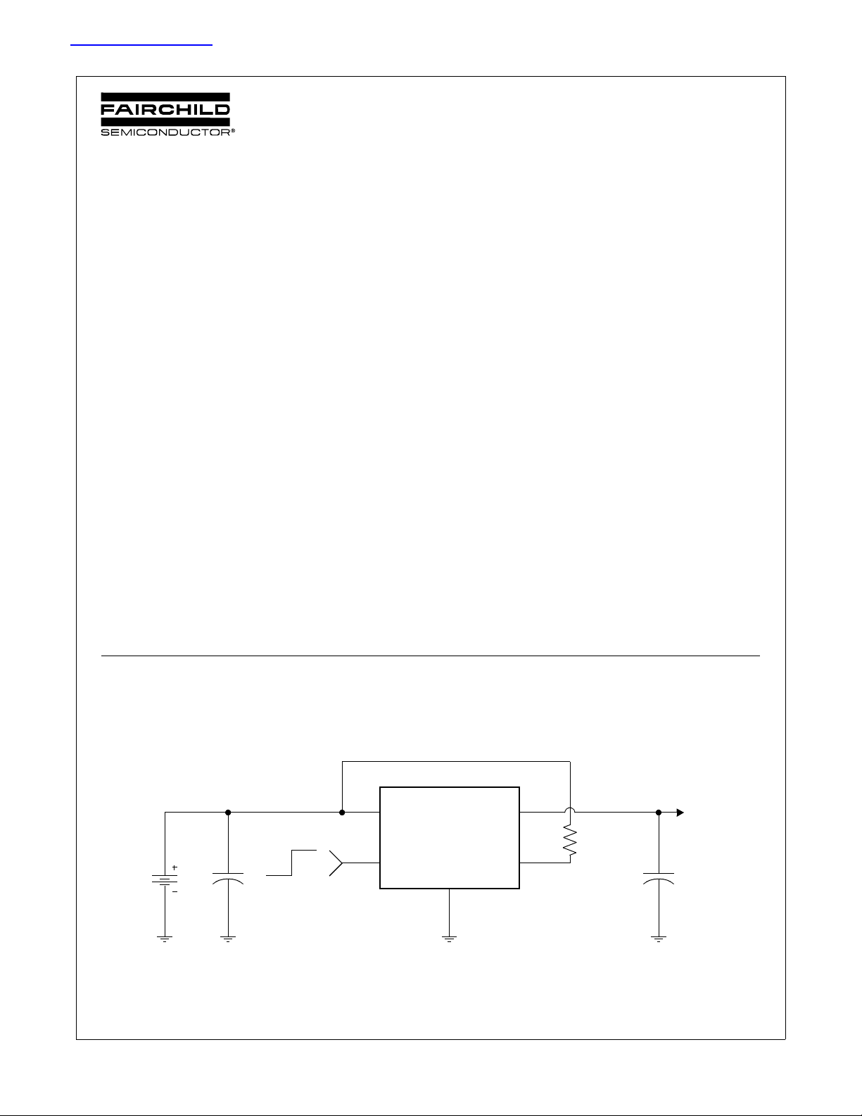
OFF ON ON
V
IN
GND
FPF2100 - FPF2107
FLAGB
V
OUT
TO LOAD
查询FPF2100供应商查询FPF2100供应商
FPF2100-FPF2107
IntelliMAX™ Advanced Load Management Products
FPF2100-FPF2107 IntelliMAX™ Advanced Load Management Products
May 2005
Features
1.8 to 5.5V Input Voltage Range
Controlled Turn-On
200mA and 400mA Current Limit Options
Undervoltage Lockout
Thermal Shutdown
<1uA Shutdown Current
Auto restart
Fast Current limit Response Time
3us to Moderate Over Currents
20ns to Hard Shorts
Fault Blanking
Applications
PDAs
Cell Phones
GPS Devices
MP3 Players
Digital Cameras
Peripheral Ports
Hot Swap Supplies
General Description
The FPF2100 through FPF2107 is a family of load switches
which provide full protection to systems and loads which may
encounter large current conditions. These devices contain a
0.125Ω current-limited P-channel MOSFET which can operate
over an input voltage range of 1.8-5.5V. Switch control is by a
logic input (ON) capable of interfacing directly with low voltage
control signals. Each part contains thermal shutdown protection
which shuts off the switch to prevent damage to the part when a
continuous over-current condition causes excessive heating.
When the switch current reaches the current limit, the part
operates in a constant-current mode to prohibit excessive
currents from causing damage. For the FPF2100-FPF2102 and
FPF2104-FPF2106, if the constant current condition still
persists after 10ms, these parts will shut off the switch and pull
the fault signal pin (FLAGB) low. The FPF2100, FPF2101,
FPF2104 and FPF2105, have an auto-restart feature which will
turn the switch on again after 160ms if the ON pin is still active.
The FPF2102 and FPF2106 do not have this auto-restart
feature so the switch will remain off until the ON pin is cycled.
For the FPF2103 and FPF2107, a current limit condition will
immediately pull the fault signal pin low and the part will remain
in the constant-current mode until the switch current falls below
the current limit. For the FPF2100 through FPF2103, the
minimum current limit is 200mA while that for the FPF2104
through FPF2107 is 400mA.
These parts are available in a space-saving 5 pin SOT23
package.
Typical Application Circuit
©2005 Fairchild Semiconductor Corporation 1 www.fairchildsemi.com
FPF2100-FPF2107 Rev. D2
Page 2
Functional Block Diagram
UVLO
THERMAL
SHUTDOWN
CURRENT
LIMIT
CONTROL
LOGIC
V
IN
ON
V
OUT
FLAGB
GND
V
IN
GND
ON
FLAGB
V
OUT
SOT23-5
1
2
3 4
5
FPF2100-FPF2107 IntelliMAX™ Advanced Load Management Products
Pin Configuration
Pin Description
Pin Name Function
1 V
2 GND Ground
3 ON ON Control Input
4 FLAGB Fault Output: Active LO, open drain output which indicates an over current supply,
5 V
IN Supply Input: Input to the power switch and the supply voltage for the IC
OUT
under voltage or over temperature state.
Switch Output: Output of the power switch
FPF2100-FPF2107 Rev. D2
2 www.fairchildsemi.com
Page 3
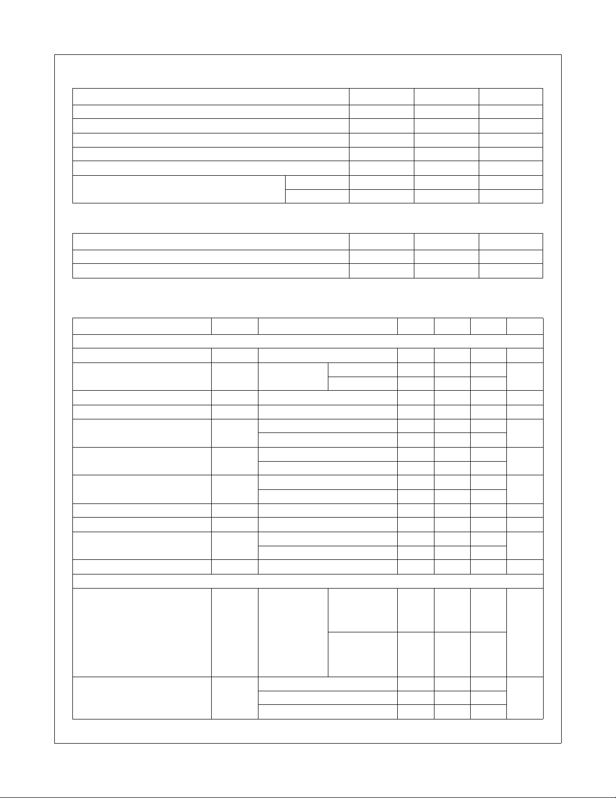
Absolute Maximum Ratings
Parameter Min. Max. Unit
VIN, V
Power Dissipation @ TA = 25°C (note 1) 667 mW
Operating Junction Temperature -40 125 °C
Storage Temperature -65 150 °C
Thermal Resistance, Junction to Ambient 150 °C/W
Electrostatic Discharge Protection HBM 4000 V
, ON, FLAGB to GND -0.3 6 V
OUT
MM 400 V
Recommended Operating Range
Parameter Min. Max. Unit
V
IN
Ambient Operating Temperature, T
A
1.8 5.5 V
-40 85 °C
Electrical Characteristics
VIN = 1.8 to 5.5V, TA = -40 to +85°C unless otherwise noted. Typical values are at VIN = 3.3V and TA = 25°C.
Parameter Symbol Conditions Min. Typ. Max Units
Basic Operation
Operating Voltage V
Quiescent Current I
IN
I
Q
= 0mA VIN = 1.8 to 3.3V 95 A
OUT
Von active VIN = 3.3 to 5.5V 110 200
Shutdown Current I
Latch-Off Current (note 2) I
On-Resistance R
ON Input Logic High Voltage V
SHDN
LATCHOFFVON
ON
TA = 25°C, I
TA = -40 to +85°C, I
IH
VIN = 1.8V 0.75 V
= VIN, after an overcurrent fault 50 A
= 50mA 125 160 m
OUT
= 50mA 150
OUT
VIN = 5.5V 1.30
ON Input Logic Low Voltage V
IL
VIN = 1.8V 0.5 V
VIN = 5.5V 1.0
ON Input Leakage VON = VIN or GND 1 A
Off Switch Leakage I
SWOFF
FLAGB Output Logic Low Voltage VIN = 5V, I
VON = 0V, V
VIN = 1.8V, I
= 0V 1 A
OUT
= 10mA 0.1 0.2 V
SINK
= 10mA 0.15 0.3
SINK
FLAGB Output High Leakage Current VIN = 5V, Switch on 1 A
Protections
Current Limit I
LIM
VIN = 3.3V,
V
= 3.0V
OUT
FPF2100,
FPF2101,
FPF2102,
FPF2103
FPF2104,
FPF2105,
FPF2106,
FPF2107
Thermal Shutdown Shutdown Threshold 140 °C
Return from Shutdown 130
Hysteresis 10
1.8 5.5 V
1 A
200 300 400 mA
400 600 800
FPF2100-FPF2107 IntelliMAX™ Advanced Load Management Products
FPF2100-FPF2107 Rev. D2
3 www.fairchildsemi.com
Page 4
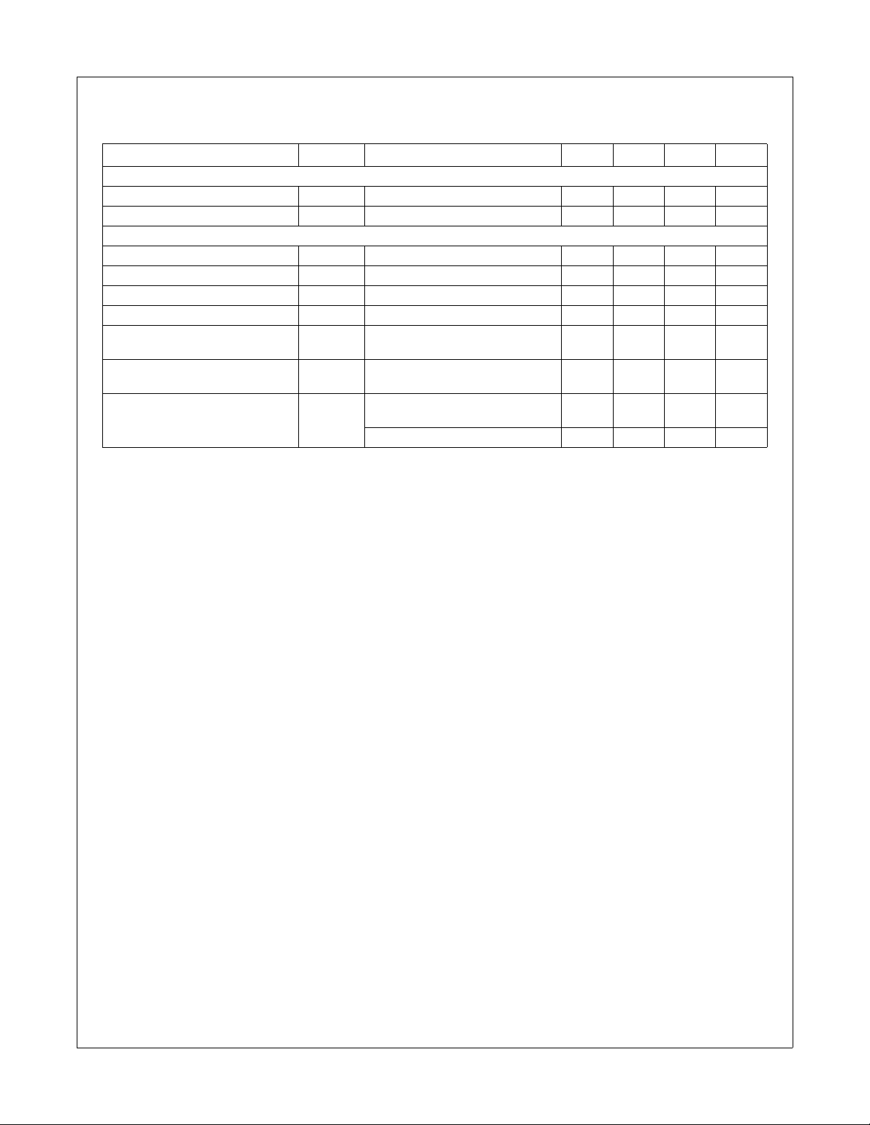
Electrical Characteristics Cont.
VIN = 1.8 to 5.5V, TA = -40 to +85°C unless otherwise noted. Typical values are at VIN = 3.3V and TA = 25°C.
Parameter Symbol Conditions Min. Typ. Max Units
Protections
Under Voltage Shutdown UVLO VIN Increasing 1.5 1.6 1.7 V
Under Voltage Shutdown Hysteresis 47 mV
Dynamic
Turn on time t
Turn off time t
V
Rise Time t
OUT
V
Fall Time t
OUT
Over Current Blanking Time t
Auto-Restart Time t
ON
OFF
R
F
BLANK
RSTRT
Short Circuit Response Time VIN = VON = 3.3V. Moderate
Note 1: Package power dissipation on 1square inch pad, 2 oz copper board.
Note 2: Applicable only to FPF2102 and FPF2106. Latchoff current does not include current flowing into FLAGB.
RL=500, CL=0.1uF 25 s
RL=500, CL=0.1uF 50 s
RL=500, CL=0.1uF 12 s
RL=500, CL=0.1uF 136 s
FPF2100, FPF2101, FPF2102,
5 10 20 ms
FPF2104, FPF2105, FPF2106
FPF2100, FPF2101, FPF2104,
80 160 320 ms
FPF2105
3 s
Over-Current Condition.
VIN = VON = 3.3V. Hard Short. 20 ns
FPF2100-FPF2107 IntelliMAX™ Advanced Load Management Products
FPF2100-FPF2107 Rev. D2
4 www.fairchildsemi.com
Page 5

Typical Characteristics
60
70
80
90
100
110
120
1.5 2 2.5 3 3.5 4 4.5 5 5.5 6
SUPPLY VOLTAGE (V)
SUPPLY CURRENT (uA)
VON = V
IN
50
70
90
110
130
150
-40 -15 10 35 60 85
TJ, JUNCTION TEMPERATURE (oC)
SUPPLY CURRENT (uA)
VIN = 1.8V
VIN = 3.3VVIN = 5.5V
0
100
200
300
400
500
600
700
-40 -15 10 35 60 85
TJ, JUNCTION TEMPERATURE (oC)
SUPPLY CURRENT (nA)
I_SHDN
VIN = 3.3V
VIN = 5.5V
0
100
200
300
400
500
-40 -15 10 35 60 85
TJ, JUNCTION TEMPERATURE (oC)
SUPPLY CURRENT (nA)
VIN = 3.3V
VIN = 5.5V
I_SWOFF
35
39
43
47
51
55
59
63
-40 -15 10 35 60 85
TJ, JUNCTION TEMPERATURE (oC)
SUPPLY CURRENT (uA)
VIN = 5.5V
VIN = 3.3V
0
0.2
0.4
0.6
0.8
1
1.2
1.4
1.5 2 2.5 3 3.5 4 4.5 5 5.5
VIN, INPUT VOLTAGE (V)
ON THRESHOLD (V)
FPF2100, 2102, 2103, 2104, 2106, 2107
FPF2101, 2105
Figure 1. Quiescent Current vs. Input Voltage Figure 2. Quiescent Current vs. Temperature
FPF2100-FPF2107 IntelliMAX™ Advanced Load Management Products
Figure 3. I
Figure 5. I
FPF2100-FPF2107 Rev. D2
SHUTDOWN
Current vs. Temperature Figure 4. I
LATCHOFF
SWITCH-OFF
Current vs. Temperature
vs. Temperature Figure 6. VIH vs. V
5 www.fairchildsemi.com
IN
Page 6

Typical Characteristics
0
100
200
300
400
500
600
700
0.3 0.6 0.9 1.2 1.5 1.8 2.1 2.4 2.7 3
VIN-V
OUT
(V)
OUTPUT CURRENT (mA)
FPF2104 - FPF2107
FPF2100 - FPF2103
100
200
300
400
500
600
700
-40 -15 10 35 60 85
TJ, JUNCTION TEMPERATURE (oC)
OUTPUT CURRENT (mA)
FPF2104 - FPF2107
FPF2100 - FPF2103
60
80
100
120
140
160
180
200
-40 -15 10 35 60 85
TJ, JUNCTION TEMPERATURE (oC)
R
ON
(mOhms)
VIN = 1.8V
VIN = 3.3V
VIN = 5.5V
90
100
110
120
130
140
150
160
1 2 3 4 5 6
VIN, INPUT VOLTAGE (V)
R
(ON)
(mOhms)
10
100
-40 -15 10 35 60 85
TJ, JUNCTION TEMPERATURE (oC)
TURN-ON/OFF TIMES (uS)
I
LOAD
= 10mA
VCC = 3.3V
TD
(ON)
TD
(OFF)
1
10
100
1000
-40 -15 10 35 60 85
TJ, JUNCTION TEMPERATURE (oC)
TURN-ON/OFF TIMES (uS)
I
LOAD
= 10mA
VCC = 3.3V
T
(FALL)
T
(RISE)
Figure 7. Current Limit vs. Output Voltage Figure 8. Current Limit vs. Temperature
FPF2100-FPF2107 IntelliMAX™ Advanced Load Management Products
Figure 9. R
Figure 11. TON/T
FPF2100-FPF2107 Rev. D2
vs. VIN Figure 10. R
(ON)
vs. Temperature Figure 12. T
Off
6 www.fairchildsemi.com
vs. Temperature
(ON)
RISE/TFALL
vs. Temperature
Page 7

Typical Characteristics
4
5
6
7
8
9
10
11
12
-40 -15 10 35 60 85
TJ, JUNCTION TEMPERATURE (oC)
FLAG-BLANKING TIME (mS)
0
20
40
60
80
100
120
140
160
180
-40 -15 10 35 60 85
TJ, JUNCTION TEMPERATURE (oC)
RESTART TIME (mS)
V
DRV
3
2V/DIV
V
OUT
2V/DIV
I
OUT
200mA/DIV
V
FLAGB
2V/DIV
V
DRV
3
2V/DIV
V
OUT
2V/DIV
I
OUT
200mA/DIV
V
FLAGB
2V/DIV
5mS/DIV
20mS/DIV
V
ON
2V/DIV
I
OUT
10mA/DIV
V
ON
2V/DIV
I
OUT
10mA/DIV
100uS/DIV 200nS/DIV
RL = 500Ω, CL = 0.1uF RL = 500Ω, CL = 0.1uF
FPF2100-FPF2107 IntelliMAX™ Advanced Load Management Products
Figure 13. T
BLANK
Figure 15. T
vs Temperature Figure 14. T
Response Figure 16. T
BLANK
RESTART
RESTART
vs Temperature
Response
Figure 17. T
FPF2100-FPF2107 Rev. D2
Response Figure 18. T
ON
7 www.fairchildsemi.com
Response
OFF
Page 8

Typical Characteristics
V
IN
2V / DIV
I
OUT
5A/DIV
V
OUT
2V/DIV
20uS/DIV 50uS/DIV
VIN/V
ON
2V/DIV
I
OUT
200mA/DIV
VIN = V
ON
CIN = 10uF
C
OUT
= 0.1uF
V
IN
2V/DIV
V
ON
2V/DIV
I
OUT
200mA/DIV
50uS/DIV
Figure 19. Short Circuit Response Time Figure 20. Current Limit Response
(Output Shorted to GND) (Switch power up to hard short)
FPF2100-FPF2107 IntelliMAX™ Advanced Load Management Products
Figure 21. Current Limit Response Time
(Output Shorted to GND by 10Ω, moderate short)
Note 3: V
FPF2100-FPF2107 Rev. D2
signal forces the device to go into overcurrent condition.
DRV
8 www.fairchildsemi.com
Page 9

FPF2100-FPF2107 IntelliMAX™ Advanced Load Management Products
Description of Operation
The FPF2100-FPF2107 are current limited switches that protect
systems and loads which can be damaged or disrupted by the
application of high currents. The core of each device is a
0.125Ω P-channel MOSFET and a controller capable of
functioning over a wide input operating range of 1.8-5.5V. The
controller protects against system malfunctions through current
limiting, under-voltage lockout and thermal shutdown. The
current limit is preset for either 200mA or 400mA.
On/OffControl
The ON pin controls the state of the switch. Active HI and LO
versions are available. Refer to the Ordering Information for
details. Activating ON continuously holds the switch in the on
state so long as there is no fault. For all versions, an
under-voltage on VIN or a junction temperature in excess of
150°C overrides the ON control to turn off the switch. In
addition, excessive currents will cause the switch to turn off in
FPF2100-FPF2102 and FPF2104-FPF2107. The FPF2100,
FPF2101, FPF2104 and FPF2105 have an Auto-Restart feature
which will automatically turn the switch on again after 160ms.
For the FPF2102 and FPF2106, the ON pin must be toggled to
turn-on the switch again. The FPF2103 and FPF2107 do not
turn off in response to a over current condition but instead
remain operating in a constant current mode so long as ON is
active and the thermal shutdown or under-voltage lockout have
not activated.
Current Limiting
The current limit ensures that the current through the switch
doesn't exceed a maximum value while not limiting at less than
a minimum value. For the FPF2100-FPF2103 the minimum
current is 200mA and the maximum current is 400mA and for
the FPF2104-FPF2107 the minimum current is 400mA and the
maximum current is 800mA. The FPF2100-FPF2103 have a
blanking time of 10ms, nominally, during which the switch will
act as a constant current source. At the end of the blanking
time, the switch will be turned-off and the FLAGB pin will
activate to indicate that current limiting has occurred. The
FPF2103 and FPF2107 have no current limit blanking period so
immediately upon a current limit condition FLAGB is activated.
These parts will remain in a constant current state until the ON
pin is deactivated or the thermal shutdown turns-off the switch.
Reverse Voltage
If the voltage at the V
curents may flow and can cause permanent damage to the
device. FPF2100-FPF2107 is designed to control current flow
from VIN to V
OUT
.
pin is larger than the VIN pin, large
OUT
Under-Voltage Lockout
The under-voltage lockout turns-off the switch if the input
voltage drops below the under-voltage lockout threshold. With
the ON pin active the input voltage rising above the
under-voltage lockout threshold will cause a controlled turn on
of the switch which limits current over-shoots.
Fault Reporting
Upon the detection of an over-current, an input under-voltage,
or an over-temperature condition, the FLAGB signals the fault
mode by activating LO. For the FPF2100-FPF2102 and
FPF2104-FPF2106, the FLAGB goes LO at the end of the
blanking time while FLAGB goes LO immediately for the
FPF2103 and FPF2107. FLAGB remains LO through the
Auto-Restart Time for the FPF2100, FPF2101 FPF2104 and
FPF2105. For the FPF2102 and FPF2106, FLAGB is latched
LO and ON must be toggled to release it.With the FPF2103 and
FPF2107, FLAGB is LO during the faults and immediately
returns HI at the end of the fault condition. FLAGB is an
open-drain MOSFET which requires a pull-up resistor between
VIN and FLAGB. During shutdown, the pull-down on FLAGB is
disabled to reduce current draw from the supply.
Thermal Shutdown
The thermal shutdown protects the part from internally or
externally generated excessive temperatures. During an
over-temperature condition the FLAGB is activated and the
switch is turned-off. The switch automatically turns-on again if
the temperature of the die drops below the threshold
temperature.
Ordering Information
Current Limit
Current Limit
Part
FPF2100 200 10 160 Active HI 2100
FPF2101 200 10 160 Active LO 2101
FPF2102 200 10 NA Active HI 2102
FPF2103 200 0 NA Active HI 2103
FPF2104 400 10 160 Active HI 2104
FPF2105 400 10 160 Active LO 2105
FPF2106 400 10 NA Active HI 2106
FPF2107 400 0 NA Active HI 2107
[mA]
Blanking Time
[ms]
Auto-Restart
Time
[ms]
ON Pin
Activity Top Mark
FPF2100-FPF2107 Rev. D2
9 www.fairchildsemi.com
Page 10

Application Information
OFF ON ON
V
IN
GND
FPF2100 - FPF2107
FLAGB
V
OUT
LOAD
Battery
1.8V-5.5V
C1 = 10µF
R1 = 100KΩ
C2 = 0.1µF
R2 = 499Ω
Input Capacitor
To limit the voltage drop on the input supply caused by transient
in-rush currents when the switch turns-on into a discharged load
capacitor or a short-circuit, a capacitor needs to be placed
between VIN and GND. A 0.1uF ceramic capacitor, CIN, placed
close to the pins is usually sufficient. Higher values of CIN can
be used to further reduce the voltage drop.
Output Capacitor
A 0.1uF capacitor C
OUT
, should be placed between V
OUT
and
GND. This capacitor will prevent parasitic board inductances
from forcing V
OUT
below GND when the switch turns-off. For
the FPF2100-FPF2102 and the FPF2104-FPF2106, the total
output capacitance needs to be kept below a maximum value,
C
OUT
(max), to prevent the part from registering an over-current
condition and turning off the switch. The maximum output
capacitance can be determined from the following formula,
Due to the integral body diode in the PMOS switch, a C
IN
greater than C
OUT
is highly recommended. A C
OUT
greater
than CIN can cause V
OUT
to exceed VIN when the system
supply is removed. This could result in current flow through the
body diode from V
OUT
to VIN.
Power Dissipation
During normal operation as a switch, the power dissipation is
small and has little effect on the operating temperature of the
part. The parts with the higher current limits will dissipate the
most power and that will only typically be,
If the part goes into current limit the maximum power dissipation
will occur when the output is shorted to ground. For the
FPF2100, FPF2101, FPF2104 and FPF2105, the power
dissipation will scale by the Auto-Restart Time, t
RSTRT
, and the
Over Current Blanking Time, t
BLANK
, so that the maximum
power dissipated is typically,
When using the FPF2102 and FPF2106 attention must be given
to the manual resetting of the part. Continuously resetting the
part at a high duty cycle when a short on the output is present
can cause the temperature of the part to increase. The junction
temperature will only be allowed to increase to the thermal
shutdown threshold. Once this temperature has been reached,
toggling ON will not turn on the switch until the junction
temperature drops. For the FPF2103 and FPF2107, a short on
the output will cause the part to operate in a constant current
state dissipating a worst case power as calculated in (3) until
the thermal shutdown activates. It will then cycle in and out of
thermal shutdown so long as the ON pin is active and the short
is present.
Board Layout
For best performance, all traces should be as short as possible.
To be most effective, the input and output capacitors should be
placed close to the device to minimize the effects that parasitic
trace inductances may have on normal and short-circuit
operation. Using wide traces for VIN, V
OUT
and GND will help
minimize parasitic electrical effects along with minimizing the
case to ambient thermal impedance.
IN
BLANKLIM
OUT
V
(min)t(max)I
(max)C
∗
=
80mW0.125(0.8)R)(I P
22
DSLIM =∗=∗=
(max)I(max)V
tt
t
P(max) LIMIN
BLANKRETRY
BLANK
∗∗
+
=
260mW0.85.5
16010
10
=∗∗
+
=
(1)
(2)
(3)
Typical Application
FPF2100-FPF2107 IntelliMAX™ Advanced Load Management Products
FPF2100-FPF2107 Rev. D2
10 www.fairchildsemi.com
Page 11

Dimensional Outline and Pad Layout
FPF2100-FPF2107 IntelliMAX™ Advanced Load Management Products
FPF2100-FPF2107 Rev. D2
11 www.fairchildsemi.com
Page 12

FPF2100-FPF2107 IntelliMAX™ Advanced Load Management Products
FPF2100-FPF2107 Rev. D2
12 www.fairchildsemi.com
 Loading...