

Page 1
■
■
■
■
■
■
■
■
■
■
■
■
■
■
■
■
查询FPF2000供应商查询FPF2000供应商
FPF2000-FPF2007 IntelliMAX™ Advanced Load Management Products
December 2004
FPF2000-FPF2007
IntelliMAX™ Advanced Load Management Products
Features
1.8 to 5.5V Input Voltage Range
Controlled Turn-On
50mA and 100mA Current Limit Options
Under voltage Lockout
Thermal Shutdown
<1uA Shutdown Current
Auto Restart
Fast Current limit Response Time
• 3us to Moderate Over Currents
• 20ns to Hard Shorts
Fault Blanking
Applications
PDAs
Cell Phones
GPS Devices
MP3 Players
Digital Cameras
Peripheral Ports
Hot Swap Supplies
General Description
The FPF2000 through FPF2007 is a family of load switches which
provide full protection to systems and loads which may encounter
large current conditions. These devices contain a 0.7 Ω current-limited P-channel MOSFET which can operate over an input voltage
range of 1.8-5.5V. Switch control is by a logic input (ON) capable of
interfacing directly with low voltage control signals. Each part contains thermal shutdown protection which shuts off the switch to prevent damage to the part when a continuous over-current condition
causes excessive heating.
When the switch current reaches the current limit, the part operates in a constant-current mode to prohibit excessive currents from
causing damage. For the FPF2000-FPF2002 and FPF2004FPF2006, if the constant current condition still persists after 10ms,
these parts will shut off the switch and pull the fault signal pin
(FLAGB) low. The FPF2000, FPF2001, FPF2004 and FPF2005,
have an auto-restart feature which will turn the switch on again
after 80ms if the ON pin is still active. The FPF2002 and FPF2006
do not have this auto-restart feature so the switch will remain off
until the ON pin is cycled. For the FPF2003 and FPF2007, a current limit condition will immediately pull the fault signal pin low and
the part will remain in the constant-current mode until the switch
current falls below the current limit. For the FPF2000 through
FPF2003, the minimum current limit is 50mA while that for the
FPF2004 through FPF2007 is 100mA.
These parts are available in a space-saving 5 pin SC-70 package.
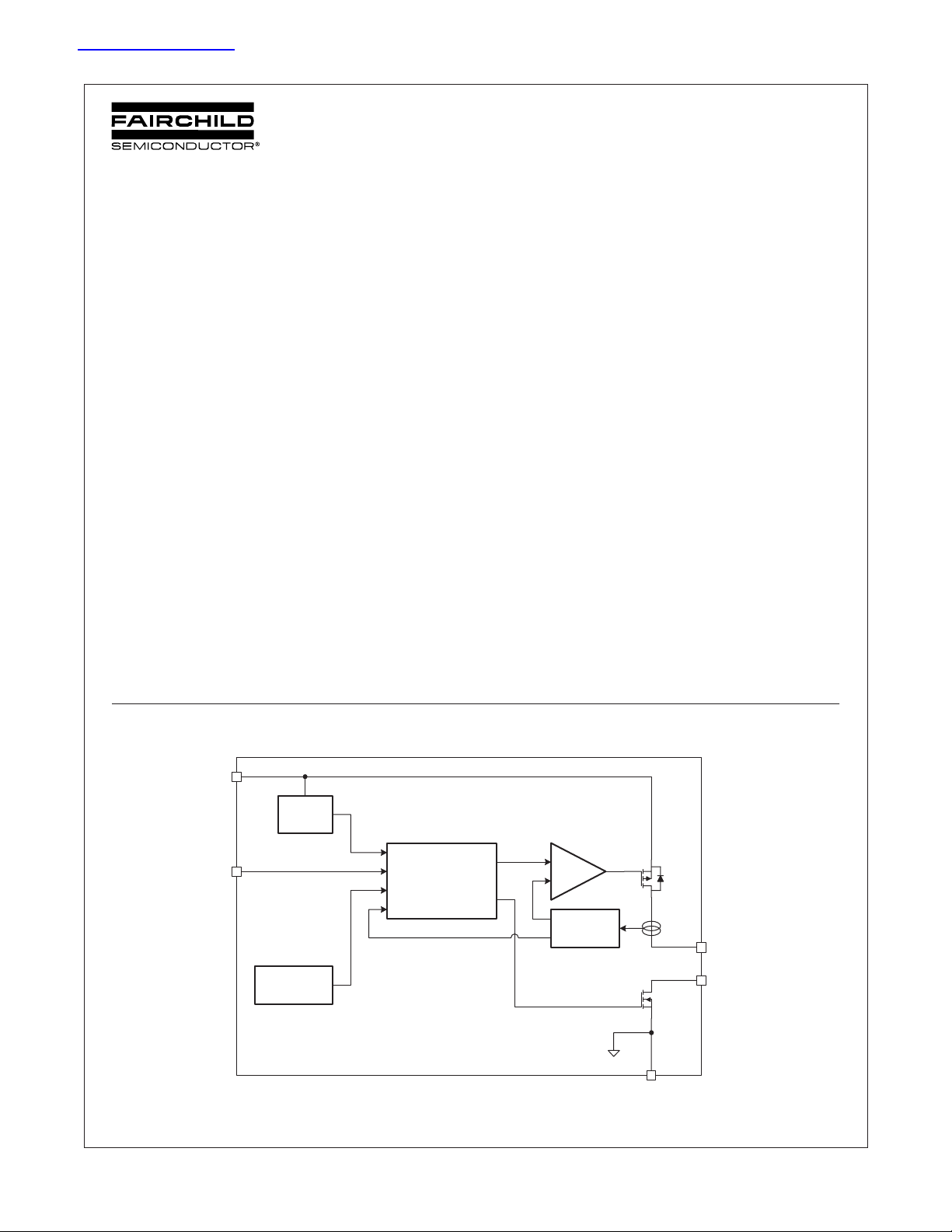
Functional Block Diagram
V
IN
ON
THERMAL
SHUTDOWN
©2004 Fairchild Semiconductor Corporation
FPF2000-FPF2007 Rev. C1
UVLO
CONTROL
LOGIC
CURRENT
LIMIT
GND
1
V
OUT
FLAGB
www.fairchildsemi.com
Page 2
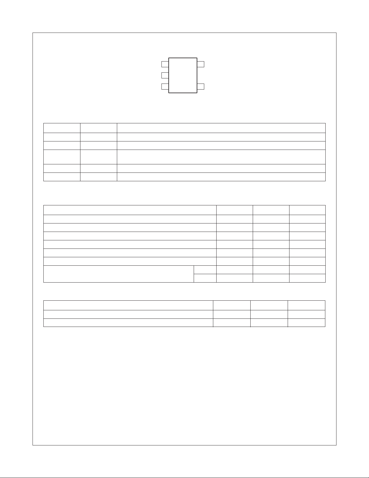
Pin Configuration
FPF2000-FPF2007 IntelliMAX™ Advanced Load Management Products
V
OUT 1
GND
FLAGB
2
34
SC70-5
5
V
IN
ON
Pin Description
Pin Name Function
1V
2 GND Ground
3 FLAGB Fault Output: Active LO, open drain output which indicates an over current, supply under voltage
4ONOn Control Input
5V
OUT
IN
Switch Output: Output of the power switch
or over temperature state.
Supply Input: Input to the power switch and the supply voltage for the IC
Absolute Maximum Ratings
Parameter Min. Max. Units
V
IN
DC Input Voltage -0.7 6 V
Power Dissipation for Single Operation @ 85°C 250 mW
Operating Junction Temperature -40 85 °C
Storage Temperature -65 150 °C
Thermal Resistance, Junction to Ambient 400 °C/W
Electrostatic Discharge Protection HBM 4000 V
MM 400 V
-0.3 6 V
Recommended Operating Range
Parameter
V
IN
Ambient Operating Temperature, T
FPF2000-FPF2007 Rev. C1
A
Min. Max. Units
1.8 5.5 V
-40 85 °C
2
www.fairchildsemi.com
Page 3
Ω
Ω
Ω
Ω
Ω
Electrical Characteristics
V
= 1.8 to 5.5V, T
IN
Parameter Symbol Conditions Min. Typ. Max. Units
Basic Operation
Operating Voltage V
Quiescent Current I
Latch-Off Current I
Shutdown Current I
On-Resistance R
ON Input Logic High Voltage V
ON Input Logic Low Voltage V
ON Input Leakage V
Off Switch Leakage I
FLAGB Output Logic Low Voltage V
FLAGB Output High Leakage Current V
Protections
Current Limit I
Thermal Shutdown T
Under Voltage Shutdown UVLO V
Under Voltage Shutdown Hysteresis 50 mV
Dynamic
Tu rn on time t
Tu rn off time t
Rise Time t
Fall Time t
OVER Current Blanking Time t
Auto-Restart Time t
Short Circuit Response Time Vin = Von = 3.3V. Moderate
= -40 to +85°C unless otherwise noted. Typical values are at V
A
IN
I
Q
LATCH
SHDN
ON
IH
IL
SWOFF
LIM
ON
OFF
RISE
FALL
BLANK
= 0mA V
OUT
FPF2002, FPF2006 40 µA
T
= 25°C, I
A
T
= -40 to +85°C, I
A
V
= 1.8V 0.5 0.66 V
IN
V
= 5.5V 0.9 1.22
IN
V
= 1.8V 0.64 0.8 V
IN
V
= 5.5V 1.17 1.5
IN
= V
or GND 1 µA
IN
= 0V, V
= 5V, I
SINK
= 1.8V, I
= 5V, Switch on 1 µA
= 3.3V,
= 0V
= 3.3V,
= 0V
Increasing 140 °C
Decreasing 130 °C
Increasing 1.5 1.6 1.7 V
V
V
V
V
V
V
T
ON
ON
IN
IN
IN
IN
OUT
IN
OUT
J
J
IN
, CL=0.1µF 50 µs
, CL=0.1µF 0.5 µs
, CL=0.1µF 10 µs
, CL=0.1µF 0.1 µs
FPF2000, FPF2001, FPF2002,
= 1.8 to 3.3V 60 µA
IN
V
= 3.3 to 5.5V 100
IN
= 20mA 0.7 1
OUT
= 20mA 0.85
OUT
= 0V 1 µA
OUT
= 10mA 0.1 0.2 V
= 10mA 0.1 0.3
SINK
FPF2000, FPF2001,
FPF2002, FPF2003
FPF2004, FPF2005,
FPF2006, FPF2007
FPF2004, FPF2005, FPF2006
RESTART
FPF2000, FPF2001, FPF2004,
FPF2005
Over-current condition.
Vin = Von = 3.3V. Hard Shorts. 20 nS
= 3.3V and T
IN
= 25°C.
A
1.8 5.5 V
1µA
50 75 100 mA
100 150 200
51020ms
40 80 160 ms
3µs
FPF2000-FPF2007 IntelliMAX™ Advanced Load Management Products
FPF2000-FPF2007 Rev. C1
3
www.fairchildsemi.com
Page 4

Typical Characteristics
FPF2000-FPF2007 IntelliMAX™ Advanced Load Management Products
75
VON =V
IN
70
A)
µ
65
60
55
QUIESCENT CURRENT (
50
11.522.533.544.555.56
SUPPLY VOLTAGE (V)
Figure 1. Quiescent Current vs. Input Voltage
160
140
120
100
80
60
40
OUTPUT CURRENT (mA)
20
0
00.30.60.91.21.51.82.12.4 2.7 33.3
FPF2004, 2005, 2006, 2007
FPF2000,2001 2002, 2003
V
- V
(V)
IN
OUT
Figure 3. Current Limit vs. Output Voltage
90
VON = V
85
80
A)
µ
75
70
65
60
55
50
QUIESCENT CURRENT (
45
40
IN
VIN = 5.5V
VIN = 3.3V
VIN = 1.8V
-40 -15 10 3 5 60 85
, JUNCTIO N TEMPERATURE ( )
T
J
°C
Figure 2. Quiescent Current vs. Temperature
35
I
SHDN
30
25
20
15
10
SHUTDOWN CURRENT (nA)
5
0
-40 -15 10 35 60 85
T
VIN = 5V
VIN = 3.3V
, JUNCTION TEMPERATURE ( )
J
°C
Figure 4. Shutdown Supply Current vs. Temperature
180
I
LIMIT
160
140
120
VIN = 3.3V
100
80
60
CURRENT LIMIT (mA)
40
20
0
-40 -15 10 35 60 85
Figure 5. Current Limit vs. Temperature
FPF2000-FPF2007 Rev. C1
1.1
1
)
0.9
Ω
FPF2004, 2005, 2006, 2007
FPF2000, 2001, 2002, 2003
, JUNCTION TEMPERATURE (°C °C
T
J
)
0.8
0.7
0.6
0.5
0.4
0.3
SWITCH RESISTANCE (
0.2
0.1
0
-40 -15 10 35 60 85
VIN = 1.8V
VIN = 3.6V
VIN = 5V
T
, JUNCTION TEMPERATURE ( )
J
Figure 6. Switch Resistance vs. Temperature
4
www.fairchildsemi.com
Page 5

Typical Characteristics
FPF2000-FPF2007 IntelliMAX™ Advanced Load Management Products
52
VIN = 3.3V
48
A)
µ
44
40
36
LATCH-O FF CURRENT (
32
28
-40 -15 10 3 5 60 85
T
, JUNCTION TEMPERATURE (°C)
J
Figure 7. Latch-Off Current vs. Temperature
1.5
1.25
FPF2000, 2002, 2003, 2004, 2006, 2007
1
0.75
0.5
ON THRESHOLD (V)
0.25
0
11.522.533.544.555.56
VIN VOLTAGE (V)
FPF2001, 2005
Figure 9. ON Threshold vs. VIN
35
30
25
20
15
10
SWITCH-OFF CURRENT (nA)
5
0
-40 -15 10 35 6 0 85
TJ, JUNCTION TEMPERATURE (°C)
VIN = 5V
VIN = 3.3V
Figure 8. Switch-Off Current vs. Temperature
CIN = 10uF
V
IN
2V/Div
I
OUT
2A/Div
V
OUT
2V/Div
= 1uF
C
OUT
20uS/Div
Figure 10. Short Circuit Response Time
(Output to GND)
100
80
60
RESTART TIME (mS)
40
-40 -15 10 35 60 85
Figure 11. Auto-Restart Time vs. Temperature
FPF2000-FPF2007 Rev. C1
JUNCTION TEMPERATURE ( )°C
T
J
V
DRV
2V/Div
V
OUT
2V/Div
I
OUT
50mA/
Div
V
FLAG
2V/Div
Figure 12. Auto-Restart Time Response
5
10mS/Div
www.fairchildsemi.com
Page 6

Typical Characteristics
FPF2000-FPF2007 IntelliMAX™ Advanced Load Management Products
100
S)
µ
10
TURN-ON/OFF TIMES (
0.1
VON
2V / DIV
I
OUT
10mA / DIV
100
I
= 10mA
LOAD
= 3.3V
V
T
I
= 10mA
LOAD
= 3.3V
V
CC
1
-40 -15 10 35 60 85
, JUNCTION TEMPERATURE (°C)
T
J
ON
T
OFF
CC
S)
µ
10
1
0.1
TURN-RISE/FALL TIMES (
0.01
-40 -15 10 35 60 85
, JUNCTION TEMPERATURE (°C)
T
J
T
Rise
T
Fall
Figure 13. Ton/Toff vs. Temperature Figure 14. Trise/Tfall vs. Temperature
V
ON
2V / DIV
I
OUT
10mA / DIV
50uS/DIV
Figure 15. Turn-On Response Figure 16. Turn-Off Response
12
V
DRV
11
10
2V / DIV
V
OUT
2V / DIV
I
9
FLAG-BLANKING TIME (mS)
8
-40 -15 10 35 60 85
T
, JUNCTION TEMPERATURE (°C)
J
OUT
2V / DIV
V
FLAG
2V / DIV
Figure 17. Blank Time vs. Temperature Figure 18. Fault Blanking Response
100nS/DIV
5mS/DIV
FPF2000-FPF2007 Rev. C1
6
www.fairchildsemi.com
Page 7

Typical Characteristics
FPF2000-FPF2007 IntelliMAX™ Advanced Load Management Products
CIN = 10uF
= 1uF
C
OUT
20uS/DIV
Figure 19. Current-Limit Response Time
(Output to GND)
V
IN
2V / DIV
V
ON
2V / DIV
I
OUT
100mA / DIV
V
OUT
(Shorted to
GND)
Description of Operation
The FPF2000-FPF2007 are current limited switches that protect
systems and loads which can be damaged or disrupted by the
application of high currents. The core of each device is a 0.7 Ω
P-channel MOSFET and a controller capable of functioning over
a wide input operating range of 1.8-5.5V. The controller protects
against system malfunctions through current limiting, undervoltage lockout and thermal shutdown. The current limit is preset for either 50mA or 100mA.
On/Off Control
The ON pin controls the state of the switch. Active HI and LO
versions are available. Refer to the Ordering Information for
details. Activating ON continuously holds the switch in the on
state so long as there is no fault. For all versions, an under-voltage on VIN or a junction temperature in excess of 150°C overrides the ON control to turn off the switch. In addition, excessive
currents will cause the switch to turn off in FPF2000-FPF2002
and FPF2004-FPF2007. The FPF2000, FPF2001, FPF2004
and FPF2005 have an Auto-Restart feature which will automatically turn the switch on again after 80ms. For the FPF2002 and
FPF2006, the ON pin must be toggled to turn-on the switch
again. The FPF2003 and FPF2007 do not turn off in response
to a over current condition but instead remain operating in a
constant current mode so long as ON is active and the thermal
shutdown or under-voltage lockout have not activated.
Fault Reporting
Upon the detection of an over-current, an input under-voltage,
or an over-temperature condition, the FLAGB signals the fault
mode by activating LO. For the FPF2000-FPF2002 and
FPF2004-FPF2006, the FLAGB goes LO at the end of the
blanking time while FLAGB goes LO immediately for the
FPF2003 and FPF2007. FLAGB remains LO through the AutoRestart Time for the FPF2000, FPF2001 FPF2004 and
FPF2005. For the FPF2002 and FPF2006, FLAGB is latched
LO and ON must be toggled to release it. With the FPF2003 and
FPF2007, FLAGB is LO during the faults and immediately
= 1uF
C
IN
= 1uF
C
OUT
V
=V
IN
ON
2V / DIV
I
OUT
100mA / DIV
20uS/DIV
Figure 20. Current-Limit Response
returns HI at the end of the fault condition. FLAGB is an opendrain MOSFET which requires a pull-up resistor between V
and FLAGB. During shutdown, the pull-down on FLAGB is disabled to reduce current draw from the supply.
Current Limiting
The current limit ensures that the current through the switch
doesn’t exceed a maximum value while not limiting at less than
a minimum value. For the FPF2000-FPF2003 the minimum current is 50mA and the maximum current is 100mA and for the
FPF2004-FPF2007 the minimum current is 100mA and the
maximum current is 200mA. The FPF2000-FPF2002 and the
FPF2004-FPF2006, have a blanking time of 10ms, nominally,
during which the switch will act as a constant current source. At
the end of the blanking time, the switch will be turned-off and
the FLAGB pin will activate to indicate that current limiting has
occurred. The FPF2003 and FPF2007 have no current limit
blanking period so immediately upon a current limit condition
FLAGB is activated. These parts will remain in a constant current state until the ON pin is deactivated or the thermal shutdown turns-off the switch.
Under-Voltage Lockout
The under-voltage lockout turns-off the switch if the input voltage drops below the under-voltage lockout threshold. With the
ON pin active the input voltage rising above the under-voltage
lockout threshold will cause a controlled turn-on of the switch
which limits current over-shoots.
Thermal Shutdown
The thermal shutdown protects the die from internally or externally generated excessive temperatures. During an over-temperature condition the FLAGB is activated and the switch is
turned-off. The switch automatically turns-on again if temperature of the die drops below the threshold temperature.
IN
FPF2000-FPF2007 Rev. C1
7
www.fairchildsemi.com
Page 8

Application Information
Typical Application
FPF2000-FPF2007 IntelliMAX™ Advanced Load Management Products
OFF ON
ON
Input Capacitor
To limit the voltage drop on the input supply caused by transient
in-rush currents when the switch turns-on into a discharged load
capacitor or a short-circuit, a capacitor needs to be placed
between V
close to the pins is usually sufficient. Higher values of C
be used to further reduce the voltage drop.
and GND. A 0.1µF ceramic capacitor, C
IN
, placed
IN
IN
can
Output Capacitor
A 0.1µF capacitor COUT, should be placed between V
GND. This capacitor will prevent parasitic board inductances
from forcing V
FPF2000-FPF2002 and the FPF2004-FPF2006, the total output
below GND when the switch turns-off. For the
OUT
capacitance needs to be kept below a maximum value,
COUT(max), to prevent the part from registering an over-current
condition and turning-off the switch. The maximum output
capacitance can be determined from the following formula,
C
OUT
max()t
LIM
=
-------------------------------------------------------------------V
IN
BLANK
min()×
I
Due to the integral body diode in the PMOS switch, a C
greater than C
C
can cause V
IN
removed. This could result in current flow through the body
diode from V
is highly recommended. A C
OUT
to exceed V
OUT
to V
OUT
.
IN
when the system supply is
IN
OUT
and
OUT
(1)
greater than
Power Dissipation
During normal operation as a switch, the power dissipation is
small and has little effect on the operating temperature of the
part. The parts with the higher current limits will dissipate the
most power and that will only be,
V
OUT
To Load
FPF2000-FPF2007
10
------------------80 10+
FLAGB
t
BLANK
-------------------------------------------------t
RESTARTtBLANK
+
5.5× 0.2× 1.22 mW=
, so that the maximum
BLANK
V
× I
IN max()
GND
Over Current Blanking Time, t
power dissipated is,
P max()
=
When using the FPF2002 and FPF2006 attention must be given
to the manual resetting of the part. Continuously resetting the
part at a high duty cycle when a short on the output is present
can cause the temperature of the part to increase. The junction
temperature will only be allowed to increase to the thermal shutdown threshold. Once this temperature has been reached, toggling ON will not turn-on the switch until the junction
temperature drops. For the FPF2003 and FPF2007, a short on
the output will cause the part to operate in a constant current
state dissipating a worst case power as calculated in (3) until
the thermal shutdown activates. It will then cycle in and out of
thermal shutdown so long as the ON pin is active and the short
is present.
Board Layout
IN
For best performance, all traces should be as short as possible.
To be most effective, the input and output capacitors should be
placed close to the device to minimize the effects that parasitic
trace inductances may have on normal and short-circuit operation. Using wide traces for V
mize parasitic electrical effects along with minimizing the case
, V
IN
and GND will help mini-
OUT
to ambient thermal impedance.
×==
LIM max()
(3)
PI
()2RDS× 0.2()20.7× 28mW===
LIM
If the part goes into current limit the maximum power dissipation
will occur when the output is shorted to ground. For the
FPF2000, FPF2001, FPF2004 and FPF2005, the power dissipation will scale by the Auto-Restart Time, t
RESTART
FPF2000-FPF2007 Rev. C1
(2)
, and the
8
www.fairchildsemi.com
Page 9

Dimensional Outline and Pad Layout
SC70-5
0.65
SYMM
C
L
FPF2000-FPF2007 IntelliMAX™ Advanced Load Management Products
(0.25)
0.65
1.00
0.80
C
GAGE PLANE
0.20
5
1
2.00±0.20
1.30
Seating Plane
0.10
0.00
A
0.30
0.15
1.25±0.10
0.10 A B
R0.10
B
M
1.10
0.80
0.10 C
0.25
0.10
1.9
1.30
LAND PATTERN RECOMMENDATION
SEE DETAIL A
(0.43)
2.10±0.10
4
3
.5 min
0.4 min
0.45
0.30
DETAIL A
NOTES:
A. THIS PACKAGE CONFORMS TO EIAJ SC-88A, 1996.
B. DIMENSIONS ARE IN MILLIMETERS.
C. DIMENSIONS DO NOT INCLUDE BURRS OR MOLD FLASH.
0°-30°
Ordering Information
Minimum
Current Limit
Part Number
FPF2000 50 10 80 Active HI 200
FPF2001 50 10 80 Active LO 201
FPF2002 50 10 NA Active HI 202
FPF2003 50 0 NA Active HI 203
FPF2004 100 10 80 Active HI 204
FPF2005 100 10 80 Active LO 205
FPF2006 100 10 NA Active HI 206
FPF2007 100 0 NA Active HI 207
[mA]
Current Limit
Blanking Time
[ms]
Auto-Restart
Time [ms] ON Pin Activity Top Mark
FPF2000-FPF2007 Rev. C1
9 www.fairchildsemi.com
Page 10

TRADEMARKS
The following are registered and unregistered trademarks Fairchild Semiconductor owns or is authorized to use and is
not intended to be an exhaustive list of all such trademarks.
ACEx™
ActiveArray™
Bottomless™
FPS™
CoolFET™
CROSSVOLT
™
DOME™
EcoSPARK™
2
CMOS™
E
EnSigna™
FACT™
FACT Quiet Series™
Across the board. Around the world.™
The Power Franchise
Programmable Active Droop™
DISCLAIMER
FAIRCHILD SEMICONDUCTOR RESERVES THE RIGHT TO MAKE CHANGES WITHOUT FURTHER NOTICE TO ANY
PRODUCTS HEREIN TO IMPROVE RELIABILITY, FUNCTION OR DESIGN. FAIRCHILD DOES NOT ASSUME ANY LIABILITY
ARISING OUT OF THE APPLICATION OR USE OF ANY PRODUCT OR CIRCUIT DESCRIBED HEREIN; NEITHER DOES IT
CONVEY ANY LICENSE UNDER ITS PATENT RIGHTS, NOR THE RIGHTS OF OTHERS.
LIFE SUPPORT POLICY
FAST
FASTr™
LittleFET™
FRFET™
GlobalOptoisolator™
GTO™
HiSeC™
2
C™
I
i-Lo
™
ImpliedDisconnect™
IntelliMAX™
ISOPLANAR™
MICROCOUPLER™
MicroFET™
MicroPak™
MICROWIRE™
MSX™
MSXPro™
OCX™
OCXPro™
OPTOLOGIC
OPTOPLANAR™
PACMAN™
POP™
Power247™
PowerEdge™
PowerSaver™
PowerTrench
QFET
QS™
QT Optoelectronics™
Quiet Series™
RapidConfigure™
RapidConnect™
µSerDes™
SILENT SWITCHER
SMART START™
SPM™
Stealth™
SuperFET™
SuperSOT™-3
SuperSOT™-6
SuperSOT™-8
SyncFET™
TinyLogic
TINYOPTO™
TruTranslation™
UHC™
UltraFET
UniFET™
VCX™
FPF2000-FPF2007 IntelliMAX™ Advanced Load Management Products
FAIRCHILD’S PRODUCTS ARE NOT AUTHORIZED FOR USE AS CRITICAL COMPONENTS IN LIFE SUPPORT
DEVICES OR SYSTEMS WITHOUT THE EXPRESS WRITTEN APPROVAL OF FAIRCHILD SEMICONDUCTOR CORPORATION.
As used herein:
1. Life support devices or systems are devices or
systems which, (a) are intended for surgical implant into
the body, or (b) support or sustain life, or (c) whose
failure to perform when properly used in accordance
with instructions for use provided in the labeling, can be
reasonably expected to result in significant injury to the
user.
PRODUCT STATUS DEFINITIONS
Definition of Terms
Datasheet Identification Product Status Definition
Advance Information
Preliminary
No Identification Needed
Formative or
In Design
First Production
Full Production
2. A critical component is any component of a life
support device or system whose failure to perform can
be reasonably expected to cause the failure of the life
support device or system, or to affect its safety or
effectiveness.
This datasheet contains the design specifications for
product development. Specifications may change in
any manner without notice.
This datasheet contains preliminary data, and
supplementary data will be published at a later date.
Fairchild Semiconductor reserves the right to make
changes at any time without notice in order to improve
design.
This datasheet contains final specifications. Fairchild
Semiconductor reserves the right to make changes at
any time without notice in order to improve design.
Obsolete
FPF2000-FPF2007 Rev. C1
Not In Production
This datasheet contains specifications on a product
that has been discontinued by Fairchild semiconductor.
The datasheet is printed for reference information only.
Rev. I15
10 www.fairchildsemi.com
 Loading...