

Page 1
FPF1107 / FPF1108
Advance Load Management Switch
FPF1107 / FPF1108 — Advance Load Management Switch
November 2009
Features
1.2V to 4V Input Voltage Operating Range
Typical R
- 35mΩ at V
- 55mΩ at V
- 85mΩ at V
Slew Rate Control with t
DS(ON)
:
=3.3V
IN
=1.8V
IN
=1.2V
IN
: 130µs
R
Output Discharge Function on FPF1108
Low <1µA Quiescent Current at V
ON=VIN
ESD Protected: Above 4000V HBM, 2000V CDM
GPIO/CMOS-Compatible Enable Circuitry
Applications
Mobile Devices and Smart Phones
Portable Media Devices
Digital Cameras
Advanced Notebook, UMPC, MID
Portable Medical Devices
GPS and Navigation Equipment
Description
The FPF1107/08 are low RDS P-channel MOSFET load
switches of the IntelliMAX™ family. Integrated slew-rate
control prevents inrush current from glitch supply rails
with capacitive loads common in power applications.
The input voltage range operates from 1.2V to 4V to
fulfill today's lowest ultra-portable device supply
requirements. Switch control is by a logic input (ON-pin)
capable of interfacing directly with low-voltage CMOS
control signals and GPIOs in embedded processors.
Ordering Information
Part
Number
FPF1107 QC 55mΩ CMOS NA
FPF1108 QD 55mΩ CMOS 65Ω
For Fairchild’s definition of Eco Status, please visit: http://www.fairchildsemi.com/company/green/rohs_green.html.
© 2009 Fairchild Semiconductor Corporation www.fairchildsemi.com
FPF1107 / FPF1108 • Rev. 1.0.1
Part
Marking
Switch
(Typical)
At 1.8V
IN
Input
Buffer
Output
Discharge
ON Pin
Activity
Active
HIGH
Active
HIGH
Eco
t
R
Status
130µs Green
130µs Green
Package
4-Ball, Wafer-Level
Chip-Scale Package
(WLCSP), 1.0 x 1.0mm,
0.5mm Pitch
Page 2
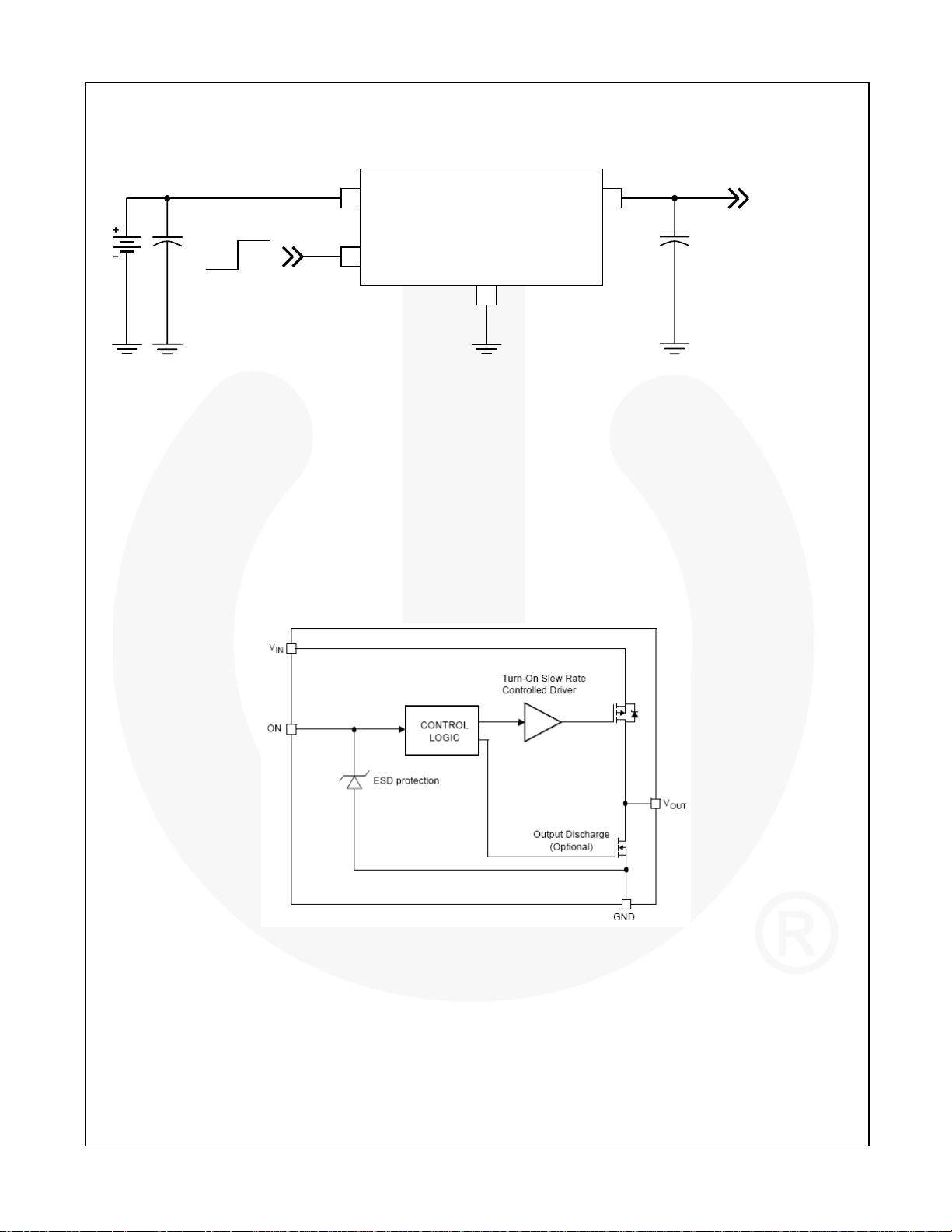
Application Diagram
FPF1107 / FPF1108 — Advance Load Management Switch
C
IN
Notes:
1. C
2. C
=1μF, X5R, 0603, for example Murata GRM185R60J105KE26
IN
=1μF, X5R, 0805, for example Murata GRM216R61A105KA01
OUT
Block Diagram
V
IN
FPF1107/FPF1108
ONOFF ON
GND
Figure 1. Typical Application
V
OUT
C
OUT
To Load
FPF1107/8
Figure 2. Block Diagram (Output Discharge for FPF1108 Only)
© 2009 Fairchild Semiconductor Corporation www.fairchildsemi.com
FPF1107 / FPF1108 • Rev. 1.0.1 2
Page 3
A2A
A
Pin Configurations
Figure 3. 1 x 1mm WLCSP Bumps Facing Down Figure 4. 1 x 1mm WLCSP Bumps Facing Up
1
V
V
OUT
A1 A2
V
IN
IN
V
OUT
FPF1107 / FPF1108 — Advance Load Management Switch
GND
Figure 5. Pin Assignments (Top View) Figure 6. Pin
B1 B2
ON
Pin Definitions
Pin # Name Description
A1 V
A2 VIN Supply Input: Input to the Power Switch.
B1 GND Ground
B2 ON ON/OFF Control, Active HIGH
Switch Output
OUT
ON
B2 B1
ssignments (Bottom View)
GND
© 2009 Fairchild Semiconductor Corporation www.fairchildsemi.com
FPF1107 / FPF1108 • Rev. 1.0.1 3
Page 4
FPF1107 / FPF1108 — Advance Load Management Switch
Absolute Maximum Ratings
Stresses exceeding the absolute maximum ratings may damage the device. The device may not function or be
operable above the recommended operating conditions and stressing the parts to these levels is not recommended.
In addition, extended exposure to stresses above the recommended operating conditions may affect device reliability.
The absolute maximum ratings are stress ratings only.
Symbol Parameter Min. Max. Unit
VIN VIN, V
ISW Maximum Continuous Switch Current 1.2 A
PD Power Dissipation at TA=25°C 1.0 W
T
Storage Junction Temperature -65 +150 °C
STG
TA Operating Temperature Range -40 +85 °C
ΘJA
ESD Electrostatic Discharge Capability
Thermal Resistance, Junction-to-Ambient
, VON to GND -0.3 4.2 V
OUT
1S2P with 1 Thermal Via 95
1S2P without Thermal Via 187
Human Body Model,
JESD22-A114
Charged Device Model,
JESD22-C101
4
2
°C/W
kV
Recommended Operating Conditions
The Recommended Operating Conditions table defines the conditions for actual device operation. Recommended
operating conditions are specified to ensure optimal performance to the datasheet specifications. Fairchild does not
recommend exceeding them or designing to Absolute Maximum Ratings.
Symbol Parameter Min. Max. Unit
VIN Supply Voltage 1.2 4.0 V
TA Ambient Operating Temperature -40 +85 °C
© 2009 Fairchild Semiconductor Corporation www.fairchildsemi.com
FPF1107 / FPF1108 • Rev. 1.0.1 4
Page 5
FPF1107 / FPF1108 — Advance Load Management Switch
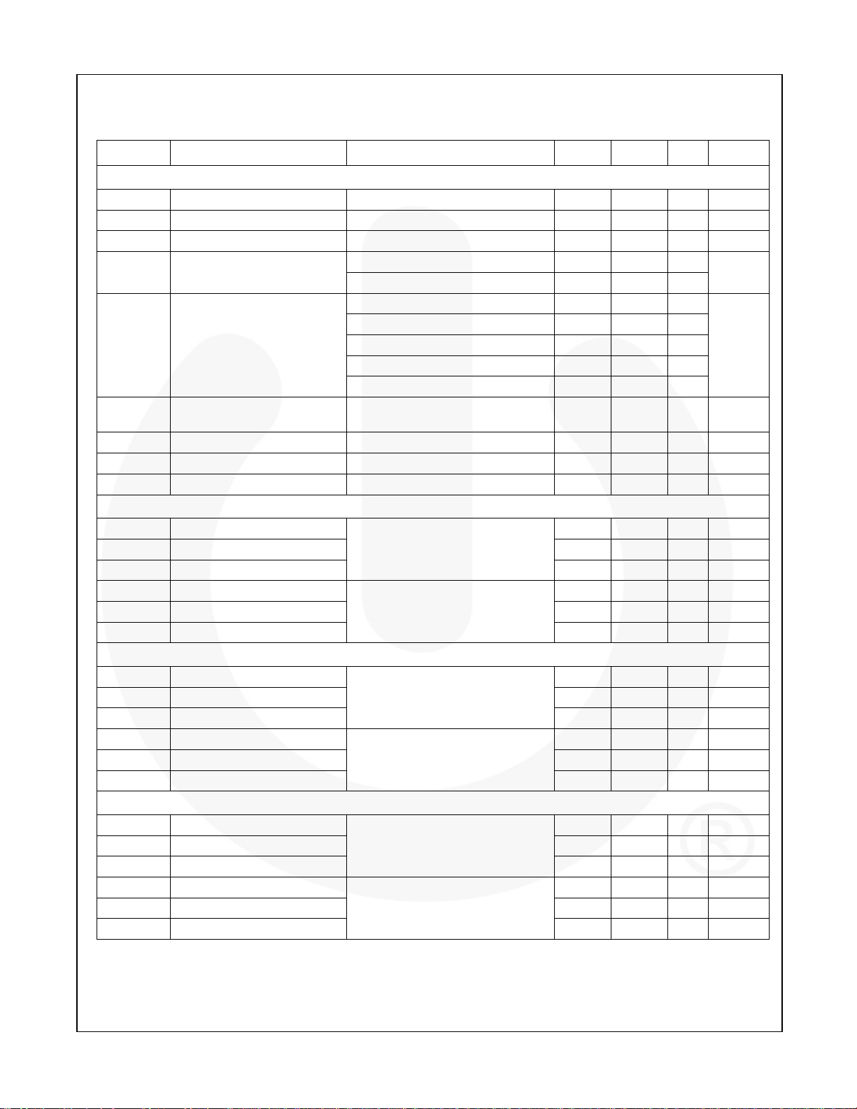
Electrical Characteristics
Unless otherwise noted, VIN=1.2 to 4.0V, TA=-40 to +85°C, typical values are at VIN=3.3V and TA=25°C.
Symbol Parameter Conditions Min. Typ. Max. Units
Basic Operation
VIN Supply Voltage 1.2 4.0 V
I
Off Supply Current VON=GND V
Q(OFF)
I
Off Switch Current VON=GND V
SD(OFF)
I
=0mA, VON=VIN 1
IQ Quiescent Current
OUT
I
=0mA, VON < VIN 3
OUT
=3.3V, I
V
IN
VIN=1.8V, I
RON On Resistance
VIN=1.5V, I
VIN=1.2V, I
VIN=1.8V, I
=3.3V, VON=0V, I
V
RPD Output Discharge R
PULL DOWN
IN
T
=25°C, FPF1108
A
VIH On Input Logic High Voltage VIN=1.2V to 4.0V 1.1 V
VIL On Input Logic Low Voltage VIN=1.2V to 4.0V 0.35 V
ION On Input Leakage VON=VIN or GND -1 1 μA
Dynamic Characteristics
t
Turn-On Delay
DON
tR V
t
ON
t
Turn-On Delay
DON
tR V
t
ON
Rise Time
OUT
Turn-On Time
Rise Time
OUT
Turn-On Time
(4)
(4,6)
(4)
(4,6)
(4)
VIN=3.3V, RL=10Ω, CL=0.1µF,
=25°C, FPF1107/8
T
A
(4)
VIN=3.3V, RL=500Ω, CL=0.1µF,
=25°C, FPF1107/8
T
A
FPF1107
t
Turn-Off Delay
DOFF
tF V
t
Turn-Off
OFF
t
Turn-Off Delay
DOFF
tF V
t
Turn-Off
OFF
FPF1108
t
Turn-Off Delay
DOFF
tF V
t
Turn-Off
OFF
t
Turn-Off Delay
DOFF
tF V
t
Turn-Off
OFF
Fall Time
OUT
Fall Time
OUT
(5)
Fall Time
OUT
Fall Time
OUT
(4)
(4)
2.2 μs
(4,7)
4.2 μs
(4)
(4)
110 μs
(4,7)
117 μs
(4)
(4)
1.9 μs
(4,7)
3.9 μs
(4)
(4)
10.6 μs
(4,7)
13.1 μs
=3.3V, RL=10Ω, CL=0.1µF,
V
IN
=25°C
T
A
=3.3V, RL=500Ω, CL=0.1µF,
V
IN
=25°C
T
A
=3.3V, RL=10Ω, CL=0.1µF,
V
IN
R
=65Ω, TA=25°C
PD
VIN=3.3V, RL=500Ω, CL=0.1µF,
=65Ω, TA=25°C
R
PD
Notes:
3. This parameter is guaranteed by design and characterization; not production tested.
4. t
DON/tDOFF/tR/tF
are defined in Figure 7.
5. Output discharge path is enabled during off.
=Open, VIN=4V 1 μA
OUT
=GND 1 μA
OUT
=200mA, TA=25°C 35 50
OUT
=200mA, TA=25°C 55 70
OUT
=200mA, TA=25°C 70
OUT
=200mA, TA=25°C 85 150
OUT
=200mA, TA=85°C
OUT
FORCE
=20mA,
(3)
65 100
65 110 Ω
80 μs
130 μs
210 μs
70 95 μs
95 120 μs
165 215 μs
2.0 2.5 μs
7.0 μs
2.0 2.5 μs
2.5 μs
μA
mΩ
© 2009 Fairchild Semiconductor Corporation www.fairchildsemi.com
FPF1107 / FPF1108 • Rev. 1.0.1 5
Page 6

V
Timing Diagram
FPF1107 / FPF1108 — Advance Load Management Switch
Notes:
6. t
ON=tR
7. t
OFF=tF
+ t
+ t
DON
DOFF
OUT
10%
90%
t
R
90%
10%
t
F
3.3V
50%
V
ON
50%
90%
t
DON
10%
t
DOFF
V
OUT
.
.
Figure 7. Timing Diagram
© 2009 Fairchild Semiconductor Corporation www.fairchildsemi.com
FPF1107 / FPF1108 • Rev. 1.0.1 6
Page 7

μ
μ
μ
μ
Typical Performance Characteristics
FPF1107 / FPF1108 — Advance Load Management Switch
0.30
A)
0.25
μ
0.20
0.15
0.10
SHUTDOWN CURRENT (
0.05
IN
V
0.00
-40 -15 10 35 60 85
, JUNCTION TEMPERATURE (°C)
T
J
VON = V
VIN= 4.0V
VIN = 3.3V
VIN = 1.2V
OUT
= 0V
0.25
A)
μ
0.20
0.15
0.10
85°C
SHUTDOWN C U R RENT (
0.05
IN
V
0.00
1.0 1.5 2.0 2.5 3.0 3.5 4.0
SUPPLY VOLTAGE (V)
VON=V
25°C
OUT
-40°C
Figure 8. Shutdown Current vs. Temperature Figure 9. Shutdown Current vs. Supply Voltage
0.10
0.09
A)
0.08
0.07
0.06
0.05
OFF SUPPLY CURRENT (
0.04
0.03
0.02
0.01
VIN = 3.3V
VIN = 1.2V
0.00
-40 -15 10 35 60 85
, JUNCTION TEMPERATURE (°C)
T
J
VON= 0V
VIN= 4.0V
0.07
VON = 0V
0.06
A)
0.05
0.04
0.03
85°C
0.02
OFF SUPPLY CURRENT (
0.01
-40°C
25°C
0.00
1.01.52.02.53.03.54.0
SUPPLY VOLTAGE (V)
=0V
Figure 10. Off Supply Current vs. Temperature
(FPF1107, VOUT is Floating)
0.050
0.045
0.040
A)
0.035
0.030
0.025
0.020
0.015
SUPPLY CURRENT (
0.010
VIN = 3.3V
0.005
0.000
-40 -15 10 35 60 85
, JUNCTION TEMPERATURE (°C)
T
J
VON = V
VIN = 4.0V
VIN= 1.2V
Figure 12. Quiescent Current vs. Temperature
(VON=VIN)
IN
Figure 11. Off Supply Current vs. Supply Voltage
(FPF1107, VOUT is Floating)
0.40
VON = V
IN
-40°C
25°C
85°C
1.01.52.02.53.03.54.0
SUPPLY VOLTAGE (V)
A)
SUPPLY CURRENT (
0.35
0.30
0.25
0.20
0.15
0.10
0.05
0.00
Figure 13. Quiescent Current vs. Supply Voltage
© 2009 Fairchild Semiconductor Corporation www.fairchildsemi.com
FPF1107 / FPF1108 • Rev. 1.0.1 7
Page 8

Y
V
(V)
T
Typical Performance Characteristics
FPF1107 / FPF1108 — Advance Load Management Switch
3.00
VON = 0.75 x V
2.50
A)
μ
2.00
1.50
1.00
SUPPLY CURRENT (
0.50
0.00
-40 -15 10 35 60 85
, JUNCTION TEMPERATURE (°C)
T
J
VIN = 4.0V
VIN = 3.3V
VIN = 1.2V
Figure 14. Quiescent Current vs. Temperature
(VON=0.75 x VIN)
120
100
)
Ω
80
60
40
ON RESISTANCE (m
20
0
-40 -15 10 35 60 85
, JUNCTION TEMPERATURE (°C)
T
J
VIN = 1.2V
VIN = 3.3V
VIN = 4.0V
VON = V
I
= 200mA
OUT
IN
2.50
2.00
1.50
1.00
0.50
SUPPLYC URRENT (µA)
0.00
1.0 1.5 2.0 2.5 3.0 3.5 4.0
+85°C
-40°C
SUPPLY VOLTAGE (V)
+25°C
Figure 15. Quiescent Current vs. Supply Voltage
at VON=1.2V
300
IN
250
)
Ω
200
150
ON RESISTANCE (m
100
85°C
25°C
50
0
-40°C
1.0 1.52.02.53.
OLT AG E
SUPPL
VON=V
IN
I
=200mA
OU
03.54.0
Figure 16. RONvs. Temperature Figure 17. RONvs. Supply Voltage
1.00
25°C
0.90
0.80
0.70
0.60
0.50
0.40
INPUT LOGIC VOLTAGE (V)
ON
0.30
V
0.20
1.0 1.5 2.0 2.5 3.0 3.5 4.0
Figure 18. ON-Pin Threshold vs. V
© 2009 Fairchild Semiconductor Corporation www.fairchildsemi.com
FPF1107 / FPF1108 • Rev. 1.0.1 8
V
IH
V
IL
SUPPLY VOLTAGE (V)
IN
Page 9

R
5
T
,
NTE
M
E(°C)
V
C
R
V
V
,
)
J
,
O
NTE
E
(°C)
V
V
y
V
y
Typical Performance Characteristics
FPF1107 / FPF1108 — Advance Load Management Switch
1000
s)
µ
t
100
VIN=3.3V
C
L
R
L
10
RISE/F ALL TIME (
t
F
1
-40 -15 10 35 60 85
T
, JUNC TION TEMPERATUR E (°C)
J
Figure 19.
Rise and Fall Time vs. Temperature
OUT
at RL=10Ω
120
110
t
s)
100
µ
90
F
t
R
80
70
RIS E/F A L L TIME (
60
50
-40 -15 10 35 60 85
JUNCTION TEMPERATURE(°C
T
Figure 21.
Rise and Fall Time vs. Temperature
OUT
VIN=3.3V
C
L
R
L
at RL=500Ω
=0.1μF
=10
=0.1μF
=500
1000
Ω
s)
µ
100
t
DON
=3.3V
IN
=0.1μF
L
=10
L
Ω
10
ON /OF F DELAYT IME (
t
DOFF
1
-40 -15 10 35 60 8
Figure 20.
JUNCTIO
Turn-On and Turn-Off Delayvs.
OUT
PERATUR
Temperature at RL=10Ω
100
90
80
s)
Ω
µ
70
t
DON
60
50
40
30
ON/OFF DELAYTIME (
20
10
t
DOFF
0
-40 -15 10 35 60 85
Figure 22.
JUN CTI
T
Turn-On and Turn-Off Dela
OUT
MPERATUR
VIN=3.3V
C
=0.1μF
L
=500
R
L
Ω
vs. Temperature at RL=500Ω
160
140
120
100
80
60
40
RISE / DELAY TIM E [µs]
20
10 100 1000
OUTPUT LO AD [ ]
Figure 23.
Turn-On and Turn-Off Dela
OUT
vs. Output Load at VIN=3.3V
© 2009 Fairchild Semiconductor Corporation www.fairchildsemi.com
FPF1107 / FPF1108 • Rev. 1.0.1 9
t
R
t
DON
Page 10

Typical Performance Characteristics
FPF1107 / FPF1108 — Advance Load Management Switch
Figure 24. Turn-On Response
(VIN=3.3V, CIN=1µF, C
=0.1µF, RL=10Ω)
OUT
Figure 26. Turn-On Response
(VIN=3.3V, CIN=1µF, C
=0.1µF, RL=500Ω)
OUT
Figure 25. Turn-Off Response
(VIN=3.3V, CIN=1µF, C
=0.1µF, RL=10Ω)
OUT
Figure 27. Turn-Off Response
(FPF1107 – No Output Pull-Down Resistor)
(VIN=3.3V, CIN=1µF, C
=0.1µF, RL=500Ω)
OUT
© 2009 Fairchild Semiconductor Corporation www.fairchildsemi.com
FPF1107 / FPF1108 • Rev. 1.0.1 10
Page 11

Application Information
FPF1107 / FPF1108 — Advance Load Management Switch
Input Capacitor
The IntelliMAXTM switch doesn’t require input capacitor.
To reduce device inrush current effect, a 0.1µF ceramic
capacitor, C
higher value of C
, is recommended close to the VIN pin. A
IN
can be used to further reduce the
IN
voltage drop experienced as the switch is turned on into
a large capacitive load.
Output Capacitor
The IntelliMAXTM switch works without an output
capacitor. However, if parasitic board inductance forces
below GND when switching off, a 0.1µF capacitor,
V
OUT
, should be placed between V
C
OUT
and GND.
OUT
Fall Time
Device output fall time can be calculated based on RC
constant of external components as follows:
2.2CRt
××=
LLF
where t
C
is 90% to 10% fall time, RL is output load and
F
is output capacitor.
L
(1)
The same equation works for a device with a pull-down
output resistor, then RL is replaced by a parallel
connected pull-down and external output resistor
combination, as follows:
RR
×
t
=
F
where t
R
=65Ω is output pull-down resistor, and CL is the
PD
PDL
RR
+
PDL
is 90% to 10% fall time, RL is output load,
F
2.2C
××
L
(2)
output capacitor.
Resistive Output Load
If resistive output load is missing, the IntelliMAXTM
switch without pull-down output resistor is not
discharging output voltage. Output voltage drop
depends, in that case, mainly on external device leaks.
© 2009 Fairchild Semiconductor Corporation www.fairchildsemi.com
FPF1107 / FPF1108 • Rev. 1.0.1 11
Page 12

Recommended Land Pattern and Layout
FPF1107 / FPF1108 — Advance Load Management Switch
For best thermal performance and minimal inductance
and parasitic effects, it is recommended to keep input
and output traces short and capacitors as close to the
device as possible. Below is a recommended layout
for this device to achieve optimum performance.
Figure 28. Recommended Land Pattern and Layout
© 2009 Fairchild Semiconductor Corporation www.fairchildsemi.com
FPF1107 / FPF1108 • Rev. 1.0.1 12
Page 13

Physical Dimensions
FPF1107 / FPF1108 — Advance Load Management Switch
2X
PIN A1 AREA
0.05
0.03 C
E
TOP VIEW
C
C
D
0.50
0.50
2
1
BOTTOM VIEW
F
A
B
D
0.03
2X
0.06 C
0.625
0.539
SEATING PLANE
0.005 CAB
Ø0.315±0.025
4X
B
(Y)±0.018
A
(X)±0.018
0.50
0.50
C
(Ø0.250)
Cu Pad
(Ø0.350)
Solder Mask
RECOMMENDED LAND PATTERN
(NSMD PAD TYPE)
0.332±0.018
0.250±0.025
SIDE VIEWS
NOTES:
A. NO JEDEC REGISTRATION APPLIES.
B. DIMENSIONS ARE IN MILLIMETERS.
F
C. DIMENSIONS AND TOLERANCES PER
ASME Y14.5M, 1994.
D. DATUM C IS DEFINED BY THE SPHERICAL
CROWNS OF THE BALLS.
E. PACKAGE NOMINAL HEIGHT IS 582 MICRONS
±43 MICRONS (539-625 MICRONS).
F. FOR DIMENSIONS D, E, X, AND Y SEE
PRODUCT DATASHEET.
G. DRAWING FILENAME: MKT-UC004ABrev2.
Figure 29. 4 Ball, 1.0 x 1.0mm Wafer Level Chip Scale WLCSP Packaging
Product-Specific Dimensions
Product D E X Y
FPF1107 960µm ± 30µm 960µm ± 30µm 0.230mm 0.230mm
FPF1108 960um ± 30µm 960um ± 30µm 0.230mm 0.230mm
Package drawings are provided as a service to customers considering Fairchild components. Drawings may change in any manner
without notice. Please note the revision and/or date on the drawing and contact a Fairchild Semiconductor representative to verify or
obtain the most recent revision. Package specifications do not expand the terms of Fairchild’s worldwide terms and conditions, specifically the
warranty therein, which covers Fairchild products.
Always visit Fairchild Semiconductor’s online packaging area for the most recent package drawings:
http://www.fairchildsemi.com/packaging/
© 2009 Fairchild Semiconductor Corporation www.fairchildsemi.com
FPF1107 / FPF1108 • Rev. 1.0.1 13
.
Page 14

FPF1107 / FPF1108 — Advance Load Management Switch
© 2009 Fairchild Semiconductor Corporation www.fairchildsemi.com
FPF1107 / FPF1108 • Rev. 1.0.1 14
Page 15

 Loading...