

Page 1
Discrete POWER & Signal
Technologies
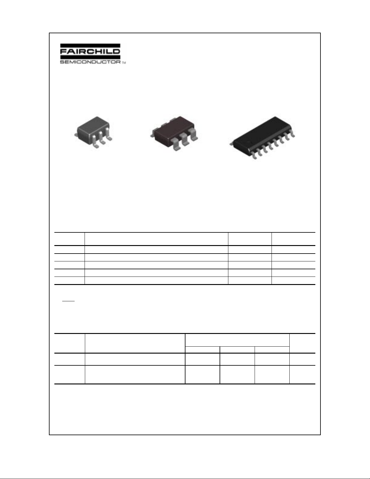
FFB3904 / FMB3904 / MMPQ3904
FFB3904
E2
B2
C1
pin #1
E1
SC70-6
Mark: .1A
B1
C2
FMB3904
C2
E1
C1
B1
pin #1
SuperSOT-6
Mark: .1A
B2
E2
MMPQ3904
B4
E4
B3
E3
B2
E2
B1
E1
C2
C1
SOIC-16
C1
C2
C3
C3
C4
NPN General Purpose Amplifier
This device is designed as a general purpose amplifier and switch.
The useful dynamic range extends to 100 mA as a switch and to
100 MHz as an amplifier. Sourced from Process 23.
Absolute Maximum Ratings* T
Symbol Parameter Value Units
V
CEO
V
CBO
V
EBO
I
C
TJ, T
stg
*These ratings are limiting values above which the serviceability of any semiconductor device may be impaired.
NOTES:
1) These ratings are based on a maximum junction temperature of 150 degrees C.
2) These are steady state limits. The factory should be consulted on applications involving pulsed or low duty cycle operations.
Collector-Emitter Voltage 40 V
Collector-Base Voltage 60 V
Emitter-Base Voltage 6.0 V
Collector Current - Continuous 200 mA
Operating and Storage Junction Temperature Range -55 to +150
= 25°C unless otherwise noted
A
C
°
C4
Thermal Characteristics T
= 25°C unless otherwise noted
A
Symbol Characteristic Max Units
FFB3904 FMB3904 MMPQ3904
P
D
R
θ
JA
1998 Fairchild Semiconductor Corporation
Total Device Dissipation
Derate above 25°C
Thermal Resistance, Junction to Ambient
Effective 4 Die
Each Die
300
2.4
700
5.6
415 180
1,000
8.0
125
240
mW
mW/°C
°C/W
°C/W
°C/W
Page 2
NPN Multi-Chip General Purpose Amplifier
(continued)
FFB3904 / FMB3904 / MMPQ3904
Electrical Characteristics T
= 25°C unless otherwise noted
A
Symbol Parameter Test Conditions Min Typ Max Units
OFF CHARACTERISTICS
V
(BR)CEO
V
(BR)CBO
V
(BR)EBO
I
BL
I
CEX
Collector-Emitter Breakdown Voltage IC = 1.0 mA, IB = 0 40 V
Collector-Base Breakdown Voltage
Emitter-Base B reakdown Voltage
I
= 10 µA, IE = 0
C
I
= 10 µA, IC = 0
E
Base Cutoff Current VCE = 30 V, V
= 0 50 nA
EB
60 V
6.0 V
Collector Cutoff Current VCE = 30 V, VEB = 0 50 nA
ON CHARACTERISTICS*
h
FE
V
V
CE(sat)
BE(sat)
DC Current Gain IC = 0.1 mA, VCE = 1.0 V
I
= 1.0 mA, VCE = 1.0 V
C
= 10 mA, VCE = 1.0 V
I
C
= 50 mA, VCE = 1.0 V
I
C
= 100 mA, VCE = 1.0 V
I
C
Collector-Emitter Saturation Voltage IC = 10 mA, IB = 1.0 mA
= 50 mA, IB = 5.0 mA
I
C
Base-Emitter Saturation Voltage IC = 10 mA, IB = 1.0 mA
= 50 mA, IB = 5.0 mA
I
C
40
70
100
300
60
30
0.2
0.3
0.65 0.85
0.95
V
V
V
V
SMALL SIGNAL CHARACTERISTICS
f
T
C
obo
C
ibo
NF Noise Figure
Current Gain - Bandwidth Product IC = 10 mA, VCE = 20 V,
f = 100 MHz
Output Capacitance VCB = 5.0 V, IE = 0,
f = 1.0 MHz
Input Capacitance VEB = 0.5 V, IC = 0,
f = 1.0 MHz
(except MMPQ3904)
IC = 100 µA, VCE = 5.0 V,
=1.0kΩ, f=10 Hz to 15.7 kHz
R
S
450 MHz
2.5 pF
6.0 pF
2.0 dB
SWITCHING CHARACTERISTICS
t
d
t
r
t
s
t
f
Delay Time VCC = 3.0 V, VBE = 0.5 V, 18 ns
Rise Time IC = 10 mA, IB1 = 1.0 mA 20 ns
Storage Time VCC = 3.0 V, IC = 10mA 150 ns
Fall Time IB1 = IB2 = 1.0 mA 25 ns
*Pulse T est: Pulse Width ≤ 300 µs, Duty Cycle ≤ 2.0%
Page 3

Typical Characteristics
FFB3904 / FMB3904 / MMPQ3904
NPN Multi-Chip General Purpose Amplifier
(continued)
Typical Pulsed Current Gain
vs Collector Current
500
400
300
125 °C
200
100
FE
h - TYPICAL PULSED CURRENT GAIN
- 40º C
0
0.1 1 10 100
I - COLLECTOR CURRENT (mA)
C
25 °C
V = 5V
CE
Base-Emitter Saturation
Voltage vs Collector Current
= 10
β
1
- 40 °C
0.8
25 °C
0.6
125 °C
0.4
BESAT
V - BASE-EMITTER VOLTAGE (V)
0.1 1 10 100
I - COLLECTOR CURRENT (mA)
C
Collector-Emi tter Saturation
Voltage vs Collector Cu rren t
V - COLLECTOR-EMITTER VOLTAGE (V)
0.15
0.1
0.05
CESAT
= 10
β
125 °C
25 °C
- 40 °C
0.1 1 10 100
I - COLLECTOR CURRENT (mA)
C
Base-Emitter ON Voltage vs
Collector Current
1
V = 5V
CE
0.8
0.6
0.4
0.2
0.1 1 10 100
BE(ON)
V - BASE-EMITTER ON VOLTAGE (V)
- 40 °C
I - COLLECTOR CURRENT (mA )
C
25 °C
125 °C
Collector-Cutoff Current
vs Ambient Temperature
500
V = 30V
100
CB
10
1
0.1
CBO
I - COLLECTOR CURRENT (nA)
25 50 75 100 125 150
T - AMBIENT TEMPERATURE ( C)
A
°
Capacitance vs
Reverse Bias Voltage
10
5
4
3
2
CAPACITANCE (pF)
1
0.1 1 10 100
REVERSE BIAS VOLTAGE (V)
f = 1.0 MHz
C
ibo
C
obo
Page 4

Typical Characteristics (continued)
FFB3904 / FMB3904 / MMPQ3904
NPN Multi-Chip General Purpose Amplifier
(continued)
Noise Figure vs Frequency
12
I = 1.0 mA
C
Ω
R = 200
10
8
6
S
I = 50 µA
R = 1.0 k
C
S
Ω
I = 0.5 mA
C
R = 200
S
Ω
V = 5.0V
CE
4
2
NF - NOISE FIGURE (dB)
0
0.1 1 10 100
I = 100 µA, R = 500
C
S
f - FREQUENCY (kHz)
Current Gain and Phase Angle
vs Frequency
50
45
40
35
30
25
20
15
10
fe
5
h - CURRENT GAIN (dB)
0
1 10 100 1000
h
fe
V = 40V
CE
I = 10 mA
C
f - FREQUENCY (MHz)
θ
Noise Figure vs Source Resistance
12
10
8
6
4
2
Ω
0
NF - NOISE FIGURE (dB)
0
0.1 1 10 100
1
20
40
θ
- DEGREES
60
0.75
80
100
120
0.5
140
160
180
0.25
D
P - POWER DISSIPATION (W)
0
0 25 50 75 100 125 150
I = 1.0 mA
C
I = 5.0 mA
C
R - SOURCE RESISTANCE ( )
S
Power Dissipation vs
Ambient Temperature
SOT-6
TEMPERATURE ( C)
I = 100 µA
C
o
I = 50 µA
C
k
Ω
Turn-On Time vs Collector Current
500
I = I =
40V
100
TIME (nS)
10
5
2.0V
t @V = 0V
d
110100
15V
t @V = 3.0V
r
CB
I - COLLECTOR CURRENT (mA)
B1CB2
CC
I
c
10
Rise Time vs Collector Current
500
T = 25°C
J
I = I =
B1CB2
V = 40V
CC
100
T = 125°C
J
r
t - RISE TIME (ns)
10
5
1 10 100
I - COLLECTOR CURRENT (mA)
I
c
10
Page 5

Typical Characteristics (continued)
FFB3904 / FMB3904 / MMPQ3904
NPN Multi-Chip General Purpose Amplifier
(continued)
Storage Time vs Collector Current
500
T = 25°C
J
S
t - STORAGE TIME (ns)
100
10
T = 125°C
J
5
1 10 100
I - COLLECTOR CURRENT (mA)
Test Circuits
300 ns
Duty Cycle
==
= 2%
==
- 0.5 V
0
<<
< 1.0 ns
<<
I = I =
B1CB2
I
c
10
10.6 V
Fall Time vs Collector Current
500
I = I =
T = 125°C
J
100
T = 25°C
J
f
t - FALL TIME (ns)
10
5
1 10 100
I - COLLECTOR CURRENT (mA)
3.0 V
ΩΩ
275
Ω
ΩΩ
ΩΩ
10 K
Ω
ΩΩ
<<
C1
< 4.0 pF
<<
B1CB2
V = 40V
CC
I
c
10
< <
10
< t
< <
1
Duty Cycle
FIGURE 1: Delay and Rise Time Equivalent Test Circuit
3.0 V
µµ
µs
µµ
0
- 9.1 V
t
1
10.9 V
<<
< 1.0 ns
<<
10 K
ΩΩ
Ω
ΩΩ
1N916
<<
< 500
<<
==
= 2%
==
FIGURE 2: Storage and Fall Time Equivalent Test Circuit
275
C1
ΩΩ
Ω
ΩΩ
<<
< 4.0 pF
<<
 Loading...