

Page 1
Discrete POWER & Signal
Technologies
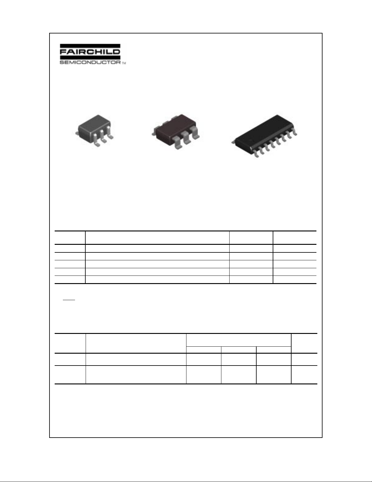
FFB2907A / FMBT2907A / MMPQ2907A
FFB2907A
E2
B2
C1
E1
B1
pin #1
SC70-6
Mark: .2F
C2
FMB2907A
C2
E1
C1
E2
B1
pin #1
SuperSOT-6
Mark: .2F
B2
MMPQ2907A
B4
E4
B3
E3
B2
E2
B1
E1
C3
C2
C2
C1
SOIC-16
C1
C3
C4
PNP Multi-Chip General Purpose Amplifier
This device is designed for use as a general purpose amplifier and switch requiring
collector currents to 500 mA. Sourced from Process 63.
Absolute Maximum Ratings* T
Symbol Parameter Value Units
V
CEO
V
CBO
V
EBO
I
C
TJ, T
stg
*These ratings are limiting values above which the serviceability of any semiconductor device may be impaired.
NOTES:
1) These ratings are based on a maximum junction temperature of 150 degrees C.
2) These are steady state limits. The factory should be consulted on applications involving pulsed or low duty cycle operations.
Collector-Emitt er Voltage 60 V
Collector-Base Voltage 60 V
Emitter-Base Volt age 5.0 V
Collector Current - Continuous 600 mA
Operating and Storage Junction Temperature Range -55 to +150
= 25°C unless otherwise noted
A
°C
C4
Thermal Characteristics T
= 25°C unless otherwise noted
A
Symbol Characteristic Max Units
FFB2907A FMB2907A MMPQ2907A
P
D
R
θ
JA
1998 Fairchild Semiconductor Corporation
Total Device Dissipation
Derate above 25°C
Thermal Resistance, Junction to Ambient
Effective 4 Die
Each Die
300
2.4
700
5.6
415 180
1,000
8.0
125
240
mW
mW/°C
°C/W
°C/W
°C/W
Page 2
PNP Multi-Chip General Purpose Amplifier
(continued)
FFB2907A / FMBT2907A / MMPQ2907A
Electrical Characteristics T
= 25°C unless otherwise noted
A
Symbol Parameter Test Conditions Min Typ Max Units
OFF CHARACTERISTICS
V
(BR)CEO
V
(BR)CBO
V
(BR)EBO
I
B
I
CEX
I
CBO
Collector-Emitt er Breakdown
IC = 10 mA, IB = 0 60 V
Voltage*
Collector-Base Breakdown Voltage
Emitter-Base Breakdown Voltage
Base Cutoff Current VCB = 30 V, V
Collector Cutoff Current VCE = 30 V, V
I
= 10 µA, IE = 0
C
I
= 10 µA, IC = 0
E
EB
BE
Collector Cutoff Current VCB = 50 V, IE = 0
= 50 V, IE = 0, TA = 125°C
V
CB
60 V
5.0 V
= 0.5 V 50 nA
= 0.5 V 50 nA
0.02
20
ON CHARACTERISTICS
h
FE
V
sat
CE(
V
sat
BE(
DC Current Gain IC = 0.1 mA, VCE = 10 V
= 1.0 mA, VCE = 10 V
I
C
= 10 mA, VCE = 10 V
I
C
= 150 mA, VCE = 10 V*
I
C
= 500 mA, VCE = 10 V*
I
Collector-Emitter Saturation Voltage* IC = 150 mA, IB = 15 mA
)
Base-Emitter Saturation Voltage IC = 150 mA, IB = 15 mA*
)
C
= 500 mA, IB = 50 mA
I
C
= 500 mA, IB = 50 mA
I
C
75
100
100
100
50
300
0.4
1.6
1.3
2.6
µA
µA
V
V
V
V
SMALL SIGNAL CHARACTERISTICS
f
T
C
obo
C
ibo
Current Gain - Bandwidth Product IC = 50 mA, VCE = 20 V,
Output Capacitance VCB = 10 V, IE = 0,
Input Capacitance VEB = 2.0 V, IC = 0,
SWITCHING CHARACTERISTICS
t
on
t
d
t
r
t
off
t
s
t
f
Turn-on Time VCC = 30 V, IC = 150 mA, 30 ns
Delay Time IB1 = 15 mA 8.0 ns
Rise Time 20 ns
Turn-off Time VCC = 6.0 V, IC = 150 mA 80 ns
Storage Time IB1 = IB2 = 15 mA 60 ns
Fall Time 20 ns
*Pulse T est: Pulse Width ≤ 300 µs, Duty Cycle ≤ 2.0%
f = 100 MHz
250 MHz
6.0 pF
f = 100 kHz
12 pF
f = 100 kHz
Page 3

T ypical Characteristics
FFB2907A / FMBT2907A / MMPQ2907A
PNP Multi-Chip General Purpose Amplifier
(continued)
T y pical Pulsed Current Gain
vs Collector Current
500
400
125 °C
300
25 °C
200
100
- 40 °C
0
0.1 0.3 1 3 10 30 100 300
FE
h - TYPICAL PULSED CURRENT GAIN
I - COLLECTOR CURRENT (mA)
C
Base-Emitter Saturation
Voltage vs Collector Current
1
- 40 ºC
0.8
0.6
0.4
0.2
25 °C
125 ºC
V = 5V
CE
= 10
β
Collector-Emi tt er Sa tu ra ti on
Voltage vs Collector Current
0.5
0.4
0.3
0.2
0.1
- COLLECTOR EMITTER VOLTAGE (V)
CESAT
= 10
β
25 °C
125 ºC
0
110100500
I - COLLECTOR CURRENT (mA)
C
- 40 ºC
Base Emitter ON Voltage vs
Collector Current
1
0.8
0.6
0.4
0.2
- 40 ºC
25 °C
125 ºC
V = 5V
CE
0
BESAT
V - BASE EMITTER VOLTAGE (V)
1 10 100 500
I - COLLECTOR CURRENT (mA)
C
Collector-Cutoff Current
vs. Ambient Temperature
100
V = 35V
CB
10
1
0.1
CBO
0.01
I - COLLECTOR CURRENT (nA)
25 50 75 100 125
T - AMBIENT TEMPERATURE ( C)
A
º
0
0.1 1 10 25
BEON
V - BASE EMITTER ON VOLT AGE (V)
I - COLLECTOR CURRENT (mA)
C
Input and Output Capacitance
vs Reverse Bias Voltage
20
16
12
8
CAPACIT ANCE (pF)
4
0
0.1 1 10 50
REVERSE BIAS VOLTAGE (V)
C
ib
C
ob
Page 4

Typical Characteristics (continued)
FFB2907A / FMBT2907A / MMPQ2907A
PNP Multi-Chip General Purpose Amplifier
(continued)
Switching Times
vs Collector Current
250
I = I =
200
V = 15 V
150
100
TIME (nS)
50
0
10 100 1000
I
B1CB2
cc
c
10
t
f
t
r
t
d
I - COLLECTOR CURRENT (mA)
t
s
Rise Time vs Collector
and Turn On Base Currents
50
20
10
t = 15 V
r
5
30 ns
2
60 ns
1
B1
10 100 500
I - TURN 0N BASE CURRENT (mA)
I - COLLECTOR CURRENT (mA)
C
Turn On and Turn Off Times
vs Collector Current
500
I = I =
400
V = 15 V
300
200
TIME (nS)
100
0
10 100 1000
1
SOT-6
0.75
0.5
0.25
D
P - POWER DISSIPATION (W)
0
0 255075100125150
I
B1CB2
cc
c
10
t
on
I - COLLECTOR CURRENT (mA)
Power Dissipation vs
Ambient Temperature
TEMPERATURE ( C)
o
t
off
Page 5

T est Circuits
PNP Multi-Chip General Purpose Amplifier
30 V
ΩΩ
200
Ω
ΩΩ
ΩΩ
1.0 K
Ω
ΩΩ
0
- 16 V
≤≤
≤ 200ns
≤≤
FIGURE 1: Saturated T urn-On Switching Time Test Circuit
50
ΩΩ
Ω
ΩΩ
FFB2907A / FMBT2907A / MMPQ2907A
(continued)
1 K
- 6.0 V
ΩΩ
Ω
ΩΩ
37
ΩΩ
Ω
ΩΩ
15 V
ΩΩ
1.0 K
Ω
ΩΩ
0
≤≤
≤ 200ns
≤≤
- 30 V
50
ΩΩ
Ω
ΩΩ
FIGURE 2: Saturated T urn-Off Switching Time T est Circuit
 Loading...