

Page 1
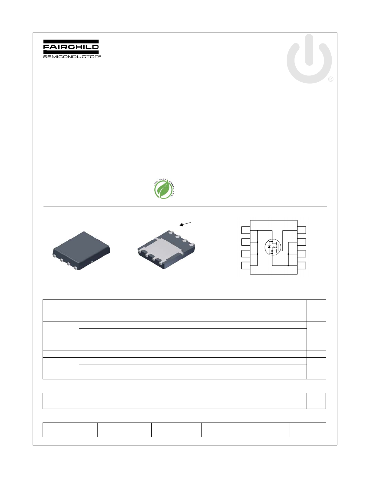
FDMS7580
N-Channel Power Trench® MOSFET
25 V, 7.5 mΩ
Features
Max r
Max r
Advanced Package and Silicon combination for low r
and high efficiency
Next generation enhanced body diode technology, engineered
for soft recovery
MSL1 robust package design
100% UIL tested
RoHS Compliant
= 7.5 mΩ at VGS = 10 V, ID = 15 A
DS(on)
= 11.1 mΩ at VGS = 4.5 V, ID = 12 A
DS(on)
DS(on)
General Description
This N-Channel MOSFET has been designed specifically to
improve the overall efficiency and to minimize switch node
ringing of DC/DC converters using either synchronous or
conventional switching PWM controllers. It has been optimized
for low gate charge, low r
diode reverse recovery performance.
Applications
Control MOSFET for Synchronous Buck Converters
Notebook
Server
Telecomm
High Efficiency DC-DC Switch Mode Power Supplies
December 2009
fast switching speed and body
DS(on),
FDMS7580 N-Channel Power Trench
®
MOSFET
Top
Power 56
D
MOSFET Maximum Ratings T
Symbol Parameter Ratings Units
V
DS
V
GS
I
D
E
AS
P
D
, T
T
J
STG
Drain to Source Voltage 25 V
Gate to Source Voltage (Note 4) ±20 V
Drain Current -Continuous (Package limited) TC = 25 °C 28
-Continuous (Silicon limited) T
-Continuous T
-Pulsed 60
Single Pulse Avalanche Energy (Note 3) 32 mJ
Power Dissipation TC = 25 °C 27
Power Dissipation T
Operating and Storage Junction Temperature Range -55 to +150 °C
Bottom
D
D
D
= 25 °C unless otherwise noted
A
Pin 1
S
S
S
G
= 25 °C 49
C
= 25 °C (Note 1a) 15
A
= 25 °C (Note 1a) 2.5
A
D
5
D
6
D
7
8
D
Thermal Characteristics
G
4
S
3
S
2
S
1
A
W
R
θJC
R
θJA
Thermal Resistance, Junction to Case 4.6
Thermal Resistance, Junction to Ambient (Note 1a) 50
Package Marking and Ordering Information
Device Marking Device Package Reel Size Tape Width Quantity
FDMS7580 FDMS7580 Power 56 13 ’’ 12 mm 3000 units
©2009 Fairchild Semiconductor Corporation
FDMS7580 Rev.C
°C/W
1
www.fairchildsemi.com
Page 2
FDMS7580 N-Channel Power Trench
Electrical Characteristics T
= 25 °C unless otherwise noted
J
Symbol Parameter Test Conditions Min Typ Max Units
Off Characteristics
BV
DSS
∆BV
DSS
∆T
J
I
DSS
I
GSS
On Characteristics
V
GS(th)
∆V
GS(th)
∆T
J
r
DS(on)
g
FS
Drain to Source Breakdown Voltage ID = 250 µA, VGS = 0 V 25 V
Breakdown Voltage Temperature
Coefficient
Zero Gate Voltage Drain Current VDS = 20 V, V
Gate to Source Leakage Current VGS = 20 V, V
ID = 250 µA, referenced to 25 °C 18 mV/°C
= 0 V 1 µA
GS
= 0 V 100 nA
DS
Gate to Source Threshold Voltage VGS = VDS, ID = 250 µA 1.0 1.6 3.0 V
Gate to Source Threshold Voltage
Temperature Coefficient
Static Drain to Source On Resistance
Forward Transconductance VDD = 5 V, ID = 15 A 63 S
ID = 250 µA, referenced to 25 °C -6 mV/°C
VGS = 10 V, ID = 15 A 5.9 7.5
VGS = 10 V, ID = 15 A, TJ = 125 °C 8.3 10.6
Dynamic Characteristics
C
iss
C
oss
C
rss
R
g
Input Capacitance
Output Capacitance 277 370 pF
Reverse Transfer Capacitance 53 80 pF
VDS = 13 V, VGS = 0 V,
f = 1 MHz
894 1190 pF
Gate Resistance 1.1 2.2 Ω
Switching Characteristics
t
d(on)
t
r
t
d(off)
t
f
Q
Q
Q
g(TOT)
gs
gd
Turn-On Delay Time
Rise Time 2.4 10 ns
Turn-Off Delay Time 17 31 ns
VDD = 13 V, ID = 15 A,
VGS = 10 V, R
GEN
= 6 Ω
7.3 15 ns
Fall Time 2.1 10 ns
Total Gate Charge VGS = 0 V to 10 V
Total Gate Charge VGS = 0 V to 4.5 V 6.5 10 nC
Total Gate Charge 2.9 nC
VDD = 13 V
ID = 15 A
14 20 nC
Gate to Drain “Miller” Charge 1.6 nC
mΩVGS = 4.5 V, ID = 12 A 8.3 11.1
®
MOSFET
Drain-Source Diode Characteristics
V
= 0 V, IS = 2 A (Note 2) 0.73 1.1
V
SD
t
rr
Q
rr
t
rr
Q
rr
NOTES:
1. R
is determined with the device mo unt ed on a 1 in2 pad 2 oz copper pad on a 1.5 x 1.5 in. boar d of FR-4 mater ial. R
θJA
the user's board design.
2. Pulse Test: Pulse Width < 300 µs, Duty cycle < 2.0 %.
of 32 mJ is based on starting TJ = 25 °C, L = 1 mH, IAS = 8 A, VDD = 23 V, VGS = 10 V. 100% test at L = 0.3 mH, IAS = 12 A.
3. E
AS
4. As an N-ch device, the negative Vgs rating is for low duty cycle pulse occurrence only. No continuous rating is implied.
FDMS7580 Rev.C
Source to Drain Diode Forward Voltage
Reverse Recovery Time
Reverse Recovery Charge 5.1 10 nC
Reverse Recovery Time
Reverse Recovery Charge 8.9 18
a. 50 °C/W when mounted on
a 1 in2 pad of 2 oz copper
GS
V
= 0 V, IS = 15 A (Note 2) 0.85 1.2
GS
IF = 15 A, di/dt = 100 A/µs
IF = 15 A, di/dt = 300 A/µs
2
19 34 ns
15 27 ns
is guaranteed by design while R
θJC
b.125 °C/W when mounted on
a minimum pad of 2 oz copper
V
is determined by
θCA
www.fairchildsemi.com
Page 3
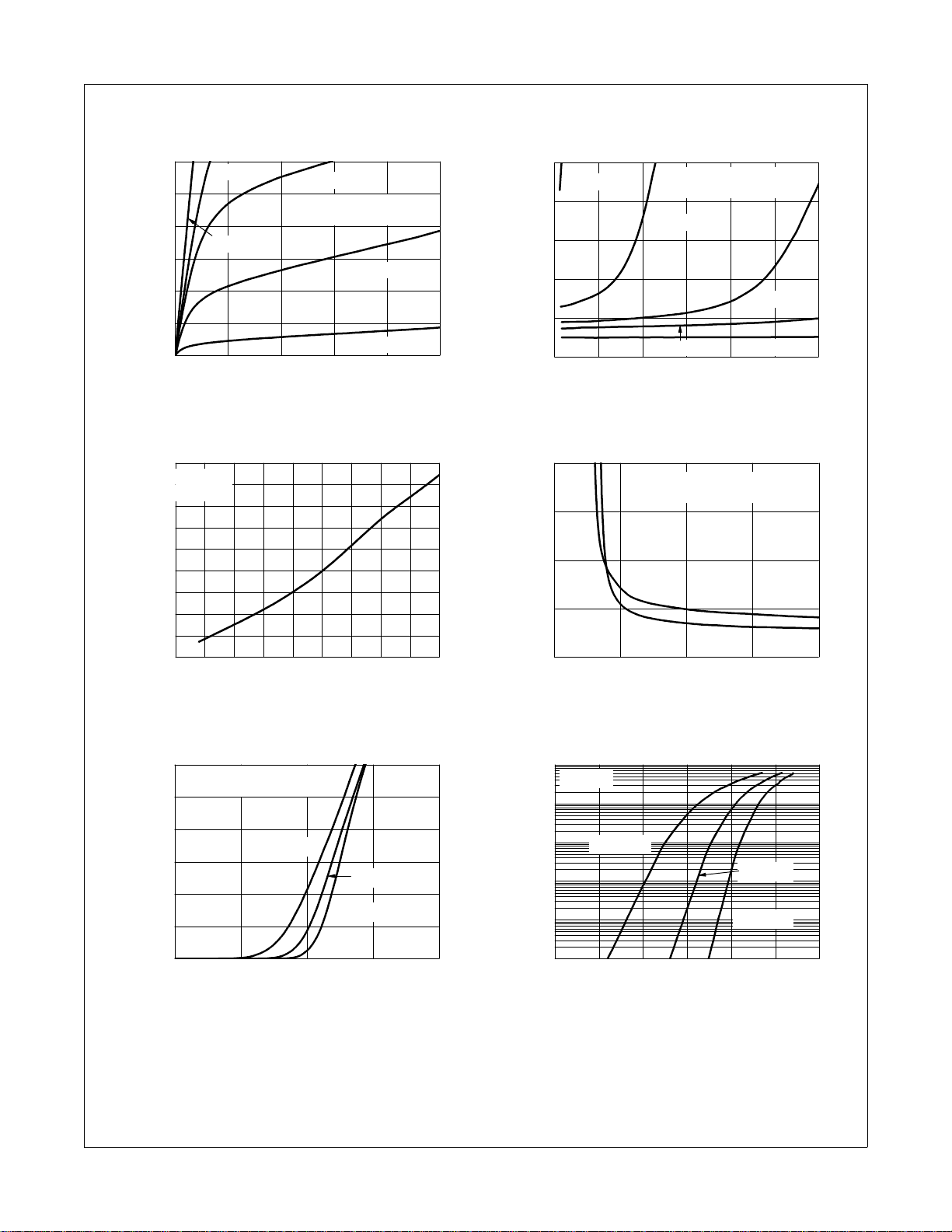
FDMS7580 N-Channel Power Trench
Typical Characteristics T
60
50
40
30
20
DRAIN CURRENT (A)
,
D
I
10
0
Figure 1.
1.6
1.5
1.4
1.3
1.2
1.1
1.0
NORMALIZED
0.9
0.8
DRAIN TO SOURCE ON-RESISTANCE
0.7
Fi gure 3 . N or ma lized On - R esistan ce
VGS = 4.5 V
VGS = 10 V
VGS = 4.0 V
PULSE DURATION = 80 µs
DUTY CYCLE = 0.5% MAX
012345
V
,
DRAIN TO SOURCE VOLTAGE (V)
DS
On-Region Characteristics Figure 2.
ID = 15 A
= 10 V
V
GS
-75 -50 -25 0 25 50 75 100 125 150
T
,
JUNCTION TEMPERATUR E
J
vs Junction Temperature
= 25 °C unless otherwise noted
J
VGS = 3.5 V
VGS = 3.0 V
o
(
C
)
10
VGS = 3.0 V
8
PULSE DURATION = 80 µs
DUTY CYCLE = 0.5% MAX
VGS = 3.5 V
6
4
NORMALIZED
VGS = 4.0 V
2
DRAIN TO SOURCE ON-RESISTANCE
0
0 102030405060
VGS = 4.5 V
I
,
DRAIN CURRENT (A)
D
VGS = 10 V
Norma liz ed On- Re sis ta nce
vs Drain Current and Gate Voltage
40
)
Ω
m
(
30
20
DRAIN TO
,
DS(on)
r
10
SOURCE ON-RESISTANCE
0
246810
Figure 4.
ID = 15 A
V
,
GATE TO S OURCE VOLTAGE (V)
GS
On-Resistance vs Gate to
PULSE DURATION = 80 µs
DUTY CYCLE = 0.5% MAX
TJ = 125 oC
TJ = 25 oC
Source Voltage
®
MOSFET
60
50
40
30
20
, DRAIN CURRENT (A)
D
I
10
FDMS7580 Rev.C
PULSE DURATION = 80 µs
DUTY CYCLE = 0.5% MAX
V
= 5 V
DS
TJ = 150 oC
TJ = 25 oC
TJ = -55 oC
0
12345
VGS, GATE TO SOURCE VOLTAGE (V)
Figure 5. Transfer Characteristics
100
V
= 0 V
GS
10
1
0.1
0.01
, REVERSE DRAIN CURRENT (A)
S
I
0.001
0.0 0 .2 0.4 0.6 0.8 1.0 1.2
TJ = 150 oC
VSD, BODY DIODE FORWARD VOLTAGE (V)
Figure 6.
Sou rce to Dr ain Diode
TJ = 25 oC
TJ = -55 oC
Forward Voltage vs Source Current
3
www.fairchildsemi.com
Page 4

FDMS7580 N-Channel Power Trench
Typical Characteristics T
10
ID = 15 A
8
VDD = 13 V
6
V
= 10 V
4
2
, GATE TO SOURCE VOLTAGE ( V)
GS
V
0
02468101214
Figure 7.
20
10
, AVALANCHE CURRENT (A)
AS
I
1
0.01 0.1 1 10 30
Figure 9.
DD
Qg, GATE CHARGE (nC)
Gate Charge Characteristics Figure 8.
TJ = 25 oC
TJ = 125 oC
tAV, TIME IN AVALANCHE (ms)
Unc lam p ed I ndu c ti v e
Switching Capability
= 25 °C unless otherwise noted
J
VDD = 16 V
TJ = 100 oC
2000
1000
100
CAPACITANCE (pF)
f = 1 MHz
= 0 V
V
GS
20
0.1 1 10 30
VDS, DRAIN TO SOURCE VOL TA G E (V)
Cap aci ta n ce v s D r ai n
to Source Voltage
50
V
= 10 V
GS
40
V
= 4.5 V
GS
30
20
DRAIN CURRENT (A)
Limited by Package
,
D
I
10
R
= 4.6 oC/W
θ
JC
0
25 50 75 100 125 150
T
,
CASE TEMPERATURE
c
Figure 10.
Ma xi mu m C on ti nu ou s D ra in
o
(
C
Current vs Case Temperature
C
iss
C
oss
C
rss
®
MOSFET
)
100
10
1
, DRAIN CURRENT (A)
0.1
D
I
0.01
0.01 0.1 1 10 100
FDMS7580 Rev.C
THIS AR E A IS
LIMITED BY r
Figure 11.
DS(on)
SINGLE PULSE
= MAX RATED
T
J
R
= 125 oC/W
θ
JA
T
= 25 oC
A
VDS, DRAIN to SOURCE VOLTAGE (V)
Forward Bias Safe
Operating Area
100 µs
1 ms
10 ms
100 ms
1 s
10 s
DC
1000
VGS = 10 V
100
SINGLE PULSE
= 125 oC/W
R
θ
JA
= 25 oC
T
A
10
PEAK TRANSIENT POWER (W)
,
)
PK
(
1
P
0.5
10-410-310-210
Figure 12.
-1
t, PULS E WIDTH (sec)
110
100 1000
Singl e Puls e Maximum
Power Dissipation
4
www.fairchildsemi.com
Page 5

FDMS7580 N-Channel Power Trench
Typical Characteristics T
2
DUTY CYCLE-DESCENDING ORDER
1
D = 0.5
0.2
0.1
0.1
0.05
0.02
0.01
SINGLE PULSE
R
θ
JA
-4
10
-3
10
JA
θ
Z
IMPEDANCE,
0.01
NORMALIZED THERMAL
0.001
= 25 °C unless otherwise noted
J
NOTES:
DUTY FACTOR: D = t
= 125 oC/W
-2
10
t, RECTANGULAR PULSE DURATION (sec)
-1
10
110
PEAK TJ = PDM x Z
Figure 13. Transient Thermal Response Curve
P
DM
t
1
t
2
1/t2
x R
+ T
θJA
θJA
A
100 1000
®
MOSFET
FDMS7580 Rev.C
5
www.fairchildsemi.com
Page 6

Dimensional Outline and Pad Layout
FDMS7580 N-Channel Power Trench
®
MOSFET
FDMS7580 Rev.C
6
www.fairchildsemi.com
Page 7

TRADEMARKS
tm
®
tm
tm
The following includes registered and unregistered trademarks and ser vice marks, owned by Fairchild Semiconductor and/or its global subsidia ries, and is not
intended to be an exhaustive list of all such trademarks.
AccuPower™
Auto-SPM™
Build it Now™
CorePLUS™
CorePOWER™
CROSSVOLT™
CTL™
Current Transfer Logic™
DEUXPEED
Dual Cool™
EcoSPARK
EfficentMax™
EZSWITCH™*
™*
Fairchild
Fairchild Semiconductor
FACT Quiet Series™
FACT
FAST
FastvCore™
FETBench™
®
®
®
®
®
®
FlashWriter
FPS™
F-PFS™
FRFET
Global Power Resource
Green FPS™
Green FPS™ e-Series™
Gmax™
GTO™
IntelliMAX™
ISOPLANAR™
MegaBuck™
MICROCOUPLER™
MicroFET™
MicroPak™
MillerDrive™
MotionMax™
Motion-SPM™
OPTOLOGIC
OPTOPLANAR
PDP SPM™
®
*
®
®
®
SM
®
Power-SPM™
PowerTrench
PowerXS™
Programmable Active Droop™
QFET
QS™
Quiet Series™
RapidConfigure™
Saving our world, 1mW/W/kW at a time™
SignalWise™
SmartMax™
SMART START™
SPM
STEALTH™
SuperFET™
SuperSOT™-3
SuperSOT™-6
SuperSOT™-8
SupreMOS™
SyncFET™
Sync-Lock™
®
®
™
®
®*
The Power Franchise
®
TinyBoost™
TinyBuck™
TinyCalc™
®
TinyLogic
TINYOPTO™
TinyPower™
TinyPWM™
TinyWire™
TriFault Detect™
TRUECURRENT™*
µSerDes™
®
UHC
Ultra FRFET™
UniFET™
VCX™
VisualMax™
®
XS™
*Trademarks of System General Corporation, used under license by Fairchild Semiconductor.
DISCLAIMER
FAIRCHILD SEMICONDUCTOR RESERVES THE RIGHT TO MAKE CHANGES WITHOUT FURTHER NOTICE TO ANY PRODUCTS HEREIN TO IMPROVE
RELIABILITY, FUNCTION, OR DESIGN. FAIRCHILD DOES NOT ASSUME ANY LIABILITY ARISING OUT OF THE APPLICATION OR USE OF ANY
PRODUCT OR CIRCUIT DESCRIBED HEREIN; NEITHER DOES IT CONVEY ANY LICENSE UNDER ITS PATENT RIGHTS, NOR THE RIGHTS OF OTHERS.
THESE SPECIFICATIONS DO NOT EXPAND THE TERMS OF FAIRCHILD’S WORLDWIDE TERMS AND CONDITIONS, SPECIFICALLY THE WARRANTY
THEREIN, WHICH COVERS THESE PRODUCTS.
FDMS7580 N-Channel Power Trench
®
MOSFET
LIFE SUPPORT POLICY
FAIRCHILD’S PRODUCTS ARE NOT AUTHORIZED FOR USE AS CRITICAL COMPONENTS IN LIFE SUPPORT DEVICES OR SYSTEMS WITHOUT THE
EXPRESS WRITTEN APPROVAL OF FAIRCHILD SEMICONDUCTOR CORPORATION.
As used herein:
1. Life support devices or systems are devices or systems which, (a) are
intended for surgical implant into the body or ( b) su pport or sustai n li fe,
and (c) whose failure to perform when properly used in accordance with
instructions for use provided in the labeling, can be reasonably
2. A critical component in any component of a life support, device, or
system whose failure to perform can be reasonably expected to cause
the failure of the life support device or system, or to affect its safety or
effectiveness.
expected to result in a significant injury of the user.
ANTI-COUNTERFEITING POLICY
Fairchild Semiconductor Corporation’s Anti-Counterfeiting Policy. Fairchild’s Anti-Counterfeiting Policy is also stated on our external website,
www.Fairchildsemi.com, under Sales Support
Counterfeiting of semiconductor parts is a growing problem in the industry. All manufact ures of semiconductor products are experiencin g counterfeiting of their
parts. Customers who inadvertently purchase counterfe it parts e xperi en ce many prob lems such a s loss of b rand rep utati on, substa nda rd perf orman ce, fa iled
application, and increased cost of production and manufacturing delays. Fairchild is taking strong measures to protect oursel ve s and our customers from the
proliferation of counterfeit parts. Fairch ild strongly encourage s custom ers to purch ase Fairchi ld parts either directly from Fa irchild or from Authorized Fairchild
Distributors who are listed by country on our web page cited above. Products customers buy either from Fairchild directly or from Authorized Fairchild
Distributors are genuine parts, have full traceability, meet Fairchild’s quality standards for handing and storage and provide access to Fairchild’s full range of
up-to-date technical and product information. Fairchild and our Authorized Distributors will stand behind all warranties and will appropriately address and
warranty issues that may arise. Fairchild will not provide any warranty coverage or other assistance for parts bought from Unauthorized Sources. Fairchild is
committed to combat this global problem and encourage o ur customers to do their part in stopping this practice b y buying direct or from authorized dist ributors.
PRODUCT STATUS DEFINITIONS
Definition of Terms
.
Datasheet Identification Product Status Definition
Advance Information Formative / In Design
Preliminary First Production
No Identification Needed Full Production
Obsolete Not In Production
FDMS7580 Rev.C 7
Datasheet contains the design specifications for product development. Specifications
may change in any manner without notice.
Datasheet contains preliminary data; supplementary data will be published at a later
date. Fairchild Semiconductor reserves the right to make changes at any time without
notice to improve design.
Datasheet contains final specifications. Fairchild Semiconductor reserves the right to
make changes at any time without notice to improve the design.
Datasheet contains specifications on a product that is discontinued by Fairchild
Semiconductor. The datasheet is for reference information only.
Rev. I45
www.fairchildsemi.com
 Loading...