

Page 1
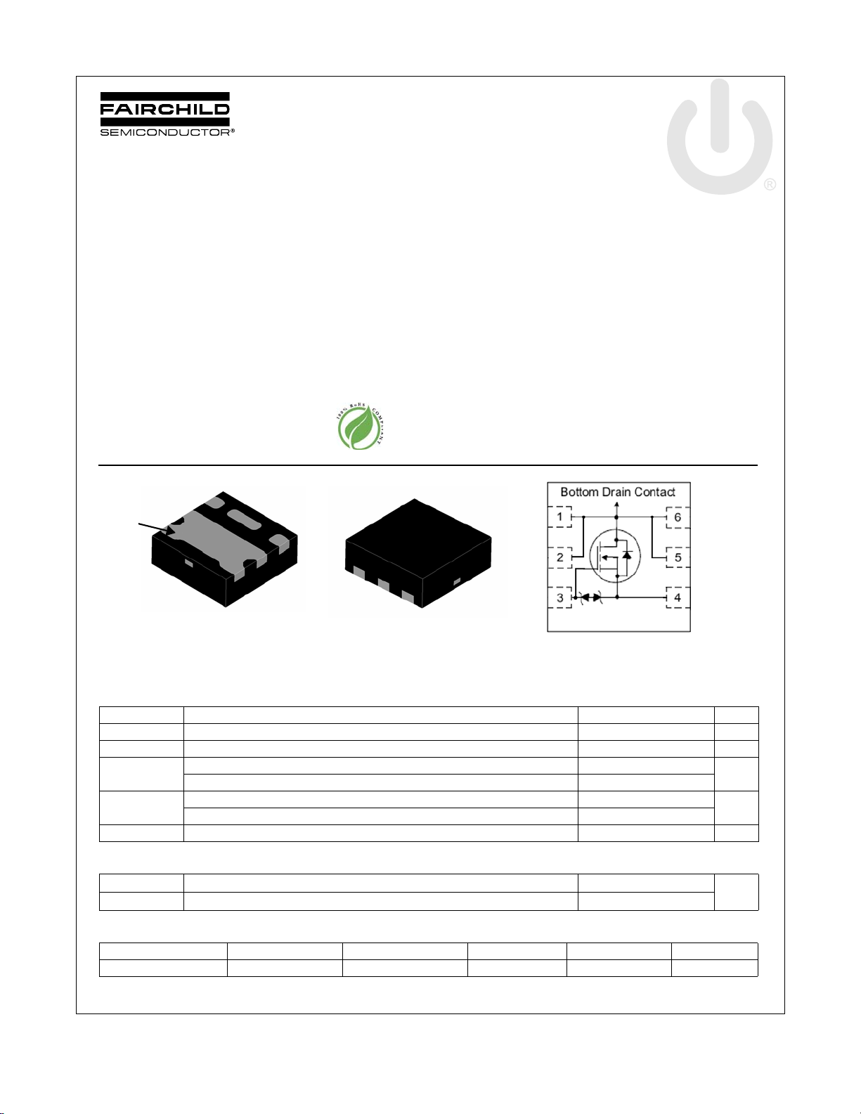
FDME820NZT
MicroFET 1.6x1.6 Thin
G
D
D
TOP
BOTTOM
Pin 1
D
G
D
S
D
D
S
D
D
N-Channel PowerTrench® MOSFET
20 V, 9 A, 18 mΩ
Features
Max r
Max r
Max r
Low profile: 0.55 mm maximum in the new package
MicroFET 1.6x1.6 Thin
Free from halogenated compounds and antimony oxides
HBM ESD protection level >2.5 kV (Note3)
RoHS Compliant
= 18 mΩ at VGS = 4.5 V, ID = 9 A
DS(on)
= 24 mΩ at VGS = 2.5 V, ID = 7.5 A
DS(on)
= 32 mΩ at VGS = 1.8 V, ID = 7 A
DS(on)
General Description
This Single N-Channel MOSFET has been designed using
Fairchild Semiconductor’s advanced Power Trench process to
optimize the r
leadframe.
DS(ON)
Applications
Li-lon Battery Pack
Baseband Switch
Load Switch
DC-DC Conversion
FDME820NZT N-Channel PowerTrench
April 2012
@ VGS = 1.8 V on special MicroFET
®
MOSFET
MOSFET Maximum Ratings T
Symbol Parameter Ratings Units
V
DS
V
GS
I
D
P
D
, T
T
J
STG
Thermal Characteristics
R
θJA
R
θJA
Package Marking and Ordering Information
©2012 Fairchild Semiconductor Corporation
FDME820NZT Rev.C
Device Marking Device Package Reel Size Tape Width Quantity
Drain to Source Voltage 20 V
Gate to Source Voltage ±12 V
Drain Current -Continuous TA = 25 °C (Note 1a) 9
-Pulsed 40
Power Dissipation for Single Operation TA = 25 °C (Note 1a) 2.1
Power Dissipation for Single Operation T
Operating and Storage Junction Temperature Range -55 to +150 °C
Thermal Resistance, Junction to Ambient (Note 1a) 70
Thermal Resistance, Junction to Ambient (Note 1b) 190
8T FDME820NZT MicroFET 1.6x1.6 Thin 7 ’’ 8 mm 5000 units
= 25 °C unless otherwise noted
A
= 25 °C (Note 1b) 0.7
A
1
A
W
°C/W
www.fairchildsemi.com
Page 2
Electrical Characteristics T
= 25 °C unless otherwise noted
J
Symbol Parameter Test Conditions Min Typ Max Units
Off Characteristics
BV
ΔBV
ΔT
I
DSS
I
GSS
DSS
DSS
J
Drain to Source Breakdown Voltage ID = 250 μA, VGS = 0 V 20 V
Breakdown Voltage Temperature
Coefficient
Zero Gate Voltage Drain Current VDS = 16 V, V
Gate to Source Leakage Current VGS = ±12 V, V
I
= 250 μA, referenced to 25 °C 20 mV/°C
D
= 0 V 1 μA
GS
= 0 V ±10 μA
DS
On Characteristics
V
GS(th)
ΔV
ΔT
r
DS(on)
GS(th)
J
Gate to Source Threshold Voltage VGS = VDS, ID = 250 μA 0.5 0.8 1.0 V
Gate to Source Threshold Voltage
Temperature Coefficient
Drain to Source On Resistance
I
= 250 μA, referenced to 25 °C -3 mV/°C
D
V
= 4.5 V, ID = 9 A 14 18
GS
= 2.5 V, ID = 7.5 A 17 24
V
GS
= 1.8 V, ID = 7 A 26 32
V
GS
= 4.5 V, ID = 9 A ,
V
GS
T
= 125 °C
J
19 24
Dynamic Characteristics
C
iss
C
oss
C
rss
R
g
Input Capacitance
Output Capacitance 203 pF
Reverse Transfer Capacitance 190 pF
= 10 V, VGS = 0 V,
V
DS
f = 1 MHz
Gate Resistance 1.0 Ω
865 pF
FDME820NZT N-Channel PowerTrench
mΩ
®
MOSFET
Switching Characteristics
t
d(on)
t
r
t
d(off)
t
f
Q
Q
Q
Q
g
g
gs
gd
Turn-On Delay Time
Rise Time 5ns
Turn-Off Delay Time 19 ns
Fall Time 5ns
Total Gate Charge VDD = 4.2 V, ID = 3 A, V
Total Gate Charge VDD = 4.2 V, ID = 3 A, V
Gate to Source Gate Charge
Gate to Drain “Miller” Charge 3.2 nC
= 10 V, ID = 4 A
V
DD
V
= 4.5 V, R
GS
= 10 V, ID = 9 A
V
DD
GEN
Drain-Source Diode Characteristics
V
= 0 V, IS = 1.6 A (Note 2) 0.7 1.2 V
V
SD
t
rr
Q
rr
Notes:
1. R
is determined with the device mounted on a 1 in2 pad 2 oz copper pad on a 1.5 x 1.5 in. bo ard of FR-4 mate rial. R
θJA
the user's board design.
Source to Drain Diode Forward Voltage
Reverse Recovery Time
Reverse Recovery Charge 4 nC
a. 70 °C/W when mounted on
a 1 in2 pad of 2 oz copper.
GS
= 0 V, IS = 9 A (Note 2) 0.8 1.2 V
V
GS
F = 9 A, di/dt = 100 A/us
I
= 2 Ω
G
9ns
= 4.3 V 8.0 nC
GS
= 4.5 V 8.5 nC
GS
1.4 nC
18 ns
is guaranteed by design while R
DF
DS
θJC
b. 190 °C/W when mounted on a
minimum pad of 2 oz copper.
SS
SF
θCA
is determined by
SS
SF
DS
G
DF
2. Pulse Test: Pulse Width < 300μs, Duty cycle < 2.0%.
3. The diode connected between the gate and source serves only as protection ESD. No gate overvoltage rating is implied.
©2012 Fairchild Semiconductor Corporation
FDME820NZT Rev.C
2
www.fairchildsemi.com
Page 3
FDME820NZT N-Channel PowerTrench
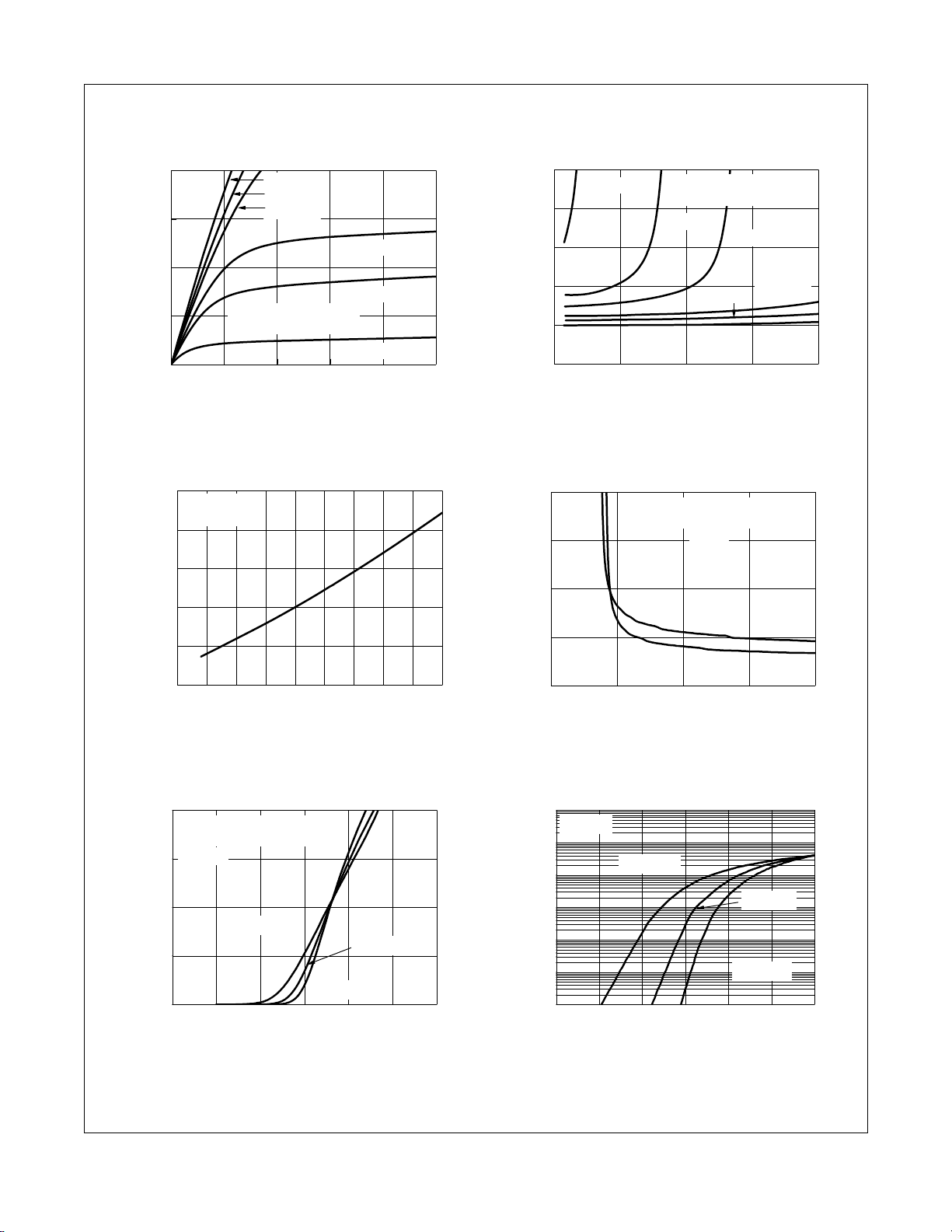
0 0.5 1.0 1.5 2.0 2.5
0
10
20
30
40
VGS = 1.5 V
VGS = 2.5 V
VGS = 1.8 V
V
DS
, DRAIN TO SOURCE VOLTAGE (V)
I
D
, DRAIN CURRENT (A)
VGS = 4.5 V
VGS = 3 V
VGS = 2 V
PULSE DURATION = 80 μs
DUTY CYCLE = 0.5% MAX
0 10203040
0
1
2
3
4
5
V
GS
= 2 V
VGS = 1.5 V
VGS = 2.5 V
PULSE DURA TION = 80 μs
DUTY CYCLE = 0.5% MAX
NORMALIZED
DRAIN TO SOURCE ON-RESISTA NCE
I
D
, DRAIN CURRENT (A)
VGS = 4.5 V
VGS = 3 V
V
GS
= 1.8 V
-75 -50 -25 0 25 50 75 100 125 150
0.6
0.8
1.0
1.2
1.4
1.6
ID = 9 A
V
GS
= 4.5 V
NORMALIZED
DRAIN TO SOURCE ON-RESISTANC E
T
J
, JUNCTION TEMPERATURE (
o
C)
0.91.82.73.64.5
0
20
40
60
80
TJ = 125 oC
ID = 9 A
TJ = 25 oC
V
GS
, GATE TO SOURCE VOLTA G E (V)
r
DS(on)
,
DRAIN TO
SOURCE ON-RESISTANCE
(mΩ)
PULSE DURATION = 80 μs
DUTY CYCLE = 0.5% MAX
0.0 0.5 1.0 1.5 2.0 2.5 3.0
0
10
20
30
40
TJ = 150 oC
V
DS
= 5 V
PULSE DURA TION = 80 μs
DUTY CYCLE = 0.5% MAX
TJ = -55 oC
TJ = 25 oC
I
D
, DRAIN CURRENT (A)
VGS, GATE TO SOURCE VOLTAGE (V)
0 0.2 0.4 0.6 0.8 1.0 1.2
0.001
0.01
0.1
1
10
100
1000
TJ = -55 oC
TJ = 25 oC
TJ = 150 oC
V
GS
= 0 V
I
S
, REVERSE DRAIN CURRENT (A)
VSD, BODY DIODE FORWARD VOLTAGE (V)
Typical Characteristics T
Figure 1.
On Region Characteristics Figure 2.
= 25 °C unless otherwise noted
J
Nor mal ized O n-R esi sta nce
vs Drain Current and Gate Voltage
®
MOSFET
Fi gure 3. N or malized On Re sistanc e
vs Junction Temperature
©2012 Fairchild Semiconductor Corporation
FDME820NZT Rev.C
Figure 5. Transfer Characteristics
Figure 4.
On-Resistance vs Ga te to
Source Voltage
Figure 6.
Source to D rain Diode
Forward Voltage vs Source Current
3
www.fairchildsemi.com
Page 4

FDME820NZT N-Channel PowerTrench
036912
0.0
0.9
1.8
2.7
3.6
4.5
ID = 9 A
VDD = 12 V
V
DD
= 10 V
V
GS
, GATE TO SOURCE VOLTAGE (V)
Qg, GATE CHARGE (nC)
VDD = 8 V
0.1 1 10 20
100
1000
2000
f = 1 MHz
V
GS
= 0 V
CAPACITANCE (pF)
VDS, DRAIN TO SOURCE VOLTAGE (V)
C
rss
C
oss
C
iss
0.001 0.01 0.1 1 10 100
1
10
20
TJ = 100 oC
TJ = 25 oC
TJ = 125 oC
tAV, TIME IN AVALANCHE (ms)
I
AS
, AVALANCHE CURRENT (A)
0369121518
10
-10
10
-9
10
-8
10
-7
10
-6
10
-5
10
-4
10
-3
10
-2
10
-1
V
GS
= 0 V
TJ = 125 oC
TJ = 25 oC
VGS, GATE TO SOURCE VOLTAGE (V)
I
g
, GATE LEAKAGE CURRENT (A)
0.01 0.1 1 10 100
0.01
0.1
1
10
100
100 us
1 ms
1 s
10 ms
DC
10 s
100 ms
I
D
, DRAIN CURRENT (A)
VDS, DRAIN to SOURCE VOLTAGE (V)
THIS AREA IS
LIMITED BY r
DS(on)
SINGLE PULSE
T
J
= MAX RATED
R
θJA
= 190
o
C/W
T
A
= 25
o
C
10-410-310-210-1110
100 1000
0.1
1
10
100
1000
SINGLE PULSE
R
θJA
= 190
o
C/W
T
A
= 25
o
C
P(
PK
), PEAK TRANSIENT POWER (W)
t, PULSE WIDTH (s)
Typical Characteristics T
Figure 7.
Gate Charge Characteristics Figure 8.
= 25 °C unless otherwise noted
J
Cap aci t anc e vs Dra in
to Source Voltage
®
MOSFET
Figure 9.
Unc l amp e d In d uct i ve
Switching Capability
©2012 Fairchild Semiconductor Corporation
FDME820NZT Rev.C
Figure 11. Forward Bias Safe
Op
erating Area
Figure 10.
Gate Leakage Current vs Gate
to Source Voltage
Figure 12.
Single P ulse Ma ximum
Power Dissipation
4
www.fairchildsemi.com
Page 5

FDME820NZT N-Channel PowerTrench
10
-4
10
-3
10
-2
10
-1
110
100 1000
0.001
0.01
0.1
1
SINGLE PULSE
R
θJA
= 190 oC/W
DUTY CYCLE-DESCENDING ORDER
NORMALIZED THERMAL
IMPEDANCE,
Z
θJA
t, RECTANGULAR PULSE DURATION (s)
D = 0.5
0.2
0.1
0.05
0.02
0.01
2
P
DM
t
1
t
2
NOTES:
DUTY FACTOR: D = t1/t
2
PEAK TJ = PDM x Z
θJA
x R
θJA
+ T
A
Typical Characteristics T
Figure 13.
= 25 °C unless otherwise noted
J
Junction-to-Ambient Transient Thermal Response Curve
®
MOSFET
©2012 Fairchild Semiconductor Corporation
FDME820NZT Rev.C
5
www.fairchildsemi.com
Page 6

Dimensional Outline and Pad Layout
BOTTOM VIEW
SIDE VIEW
TOP VIEW
RECOMMENDED LAND PATTERN OPT 1
0.10 C A B
0.05 C
0.10 C
0.08 C
C
1.60
1.60
0.10 C
2X
2X
0.10
C
(0.15)
0.50
1.00
0.72
0.62
(0.20)
PIN #1 I DEN T
(0.125)
(0.40)
RECOMMENDED LAND PATTERN OPT 2
NOTES:
A. DOES NOT FULLY CONFORM TO JEDEC
REGISTRATION
B. DIMEN SION S ARE IN MILLI METERS .
C. DIMENSIONS AND TOLERANCES PER
ASME Y14.5M , 1994.
D. LAND PATTERN RECOMMEND ATION IS
BASED ON FSC DESIGN ONLY
E. DRAWING FILENAME: MKT-UMLP06Frev4
13
46
46
3
1
0.55
0.40
1.90
0.65
No vias or traces
allowed in
thi s ar e a
0.15
0.670
0.570
0.30
0.20
2X
0.05
0.00
0.55 MAX
(0.55)
0.30
0.20
2X
0.50
0.30
0.35
4
6
31
0.55
(0.4 0)
1.90
0.65
0.15
0.50
0.30
0.35
0.62
0.20
No vias or traces
allowed in
th is ar ea
1.150
1.050
FDME820NZT N-Channel PowerTrench
®
MOSFET
©2012 Fairchild Semiconductor Corporation
FDME820NZT Rev.C
6
www.fairchildsemi.com
Page 7

TRADEMARKS
®
™
tm
tm
The following includes registered and unregistered trademarks a nd service marks, owned by Fairch ild Semiconductor and/ or its global subsidiaries, and is n ot
intended to be an exhaustive list of all such trademarks.
2Cool™
AccuPower™
AX-CAP™*
®
BitSiC
Build it Now™
CorePLUS™
CorePOWER™
CROSSVOLT™
CTL™
Current Transfer Logic™
DEUXPEED
Dual Cool™
EcoSPARK
EfficentMax™
ESBC™
Fairchild
Fairchild Semiconductor
FACT Quiet Series™
FACT
FAST
FastvCore™
FETBench™
FlashWriter
FPS™
®
®
®
®
®
®
*
®
F-PFS™
®
FRFET
Global Power Resource
Green Bridge™
Green FPS™
Green FPS™ e-Series™
Gmax™
GTO™
IntelliMAX™
ISOPLANAR™
Marking Small Speakers Sound Louder
and Better™
MegaBuck™
MICROCOUPLER™
MicroFET™
MicroPak™
MicroPak2™
MillerDrive™
MotionMax™
Motion-SPM™
mWSaver™
OptoHiT™
OPTOLOGIC
OPTOPLANAR
®
®
®
SM
PowerTrench
PowerXS™
Programmable Active Droop™
QFET
QS™
Quiet Series™
RapidConfigure™
Saving our world, 1mW/W/kW at a time™
SignalWise™
SmartMax™
SMART START™
Solutions for Your Success™
SPM
STEALTH™
SuperFET
SuperSOT™-3
SuperSOT™-6
SuperSOT™-8
SupreMOS
SyncFET™
Sync-Lock™
®
®
®
®
®
®*
The Power Franchise
TinyBoost™
TinyBuck™
TinyCalc™
®
TinyLogic
TINYOPTO™
TinyPower™
TinyPWM™
TinyWire™
®
TranSiC
TriFault Detect™
TRUECURRENT
μSerDes™
®
UHC
Ultra FRFET™
UniFET™
VCX™
VisualMax™
VoltagePlus™
XS™
®
®
®
*
*Trademarks of System General Corporation, used under license by Fairchild Semiconductor.
DISCLAIMER
FAIRCHILD SEMICONDUCTOR RESERVES THE RIGHT TO MAKE CHANGES WITHOUT FURTHER NOTICE TO ANY PRODUCTS HEREIN TO IMPROVE
RELIABILITY, FUNCTION, OR DESIGN. FAIRCHILD DOES NOT ASSUME ANY LIABILITY ARISING OUT OF THE APPLICATION OR USE OF ANY
PRODUCT OR CIRCUIT DESCRIBED HEREIN; NEITHER DOES IT CONVEY ANY LICENSE UNDER ITS PATENT RIGHTS, NOR THE RIGHTS OF OTHERS.
THESE SPECIFICATIONS DO NOT EXPAND THE TERMS OF FAIRCHILD’S WORLDWIDE TERMS AND CONDITIONS, SPECIFICALLY THE WARRANTY
THEREIN, WHICH COVERS THESE PRODUCTS.
FDME820NZT N-Channel PowerTrench
®
MOSFET
LIFE SUPPORT POLICY
FAIRCHILD’S PRODUCTS ARE NOT AUTHORIZED FOR USE AS CRITICAL COMPONENTS IN LIFE SUPPORT DEVICES OR SYSTEMS WITHOUT THE
EXPRESS WRITTEN APPROVAL OF FAIRCHILD SEMICONDUCTOR CORPORATION.
As used here in:
1. Life support devices or systems are devices or systems which, (a) are
intended for surgical implant into the bo dy or (b ) support or su stain life,
and (c) whose failure to perform when properly used in accordan ce with
instructions for use provided in the labeling, can be reasonably
expected to result in a significant injury of the user.
ANTI-COUNTERFEITING POLICY
Fairchild Semiconductor Corporation’s Anti-Counterfeiting Policy. Fairchild’s Anti-Counterfeiting Policy is also stated on our external website,
www.Fairchildsemi.com, under Sales Support
Counterfeiting of semiconductor parts is a growing problem in the industry. All manufactures of semiconductor products are exper iencing counterfeiting of their
parts. Customers who inadvertently purchase counterfeit part s expe rience many problems such as loss of brand repu tation, substa ndar d pe rformance, fail ed
application, and increased cost of production and manufacturing delays. Fairchild is taki ng st ron g measures to prote ct ourselves and our custo mers from the
proliferation of counterfeit parts. Fairchild strongl y encourages customers t o purchase Fairchil d parts either d irectly from Fairchild o r from Authorized Fairchi ld
Distributors who are listed by country on our web page cited above. Products customers buy either from Fairchild directly or from Authorized Fairchild
Distributors are genuine parts, have full traceability, meet Fairchild’s quality standards for handing and storage and provide access t o Fairchild’s full range of
up-to-date technical and product information. Fairchild and our Authorized Distributors will stand behind all warranties and will appropriately address and
warranty issues that may arise. Fairchild will not provide any warranty coverage or other assistance for parts bought from Unauthorized Sources. Fairchild is
.
2. A critical component in any component of a life support, device, or
system whose failure to perform can be reasonably expected to cause
the failure of the life support device or system, or to affect its safety or
effectiveness.
committed to combat this global problem and encourage our customers to do their part in stopping this practi ce by buying direct or fr om authorized distributors.
PRODUCT STATUS DEFINITIONS
Definition of Terms
Datasheet Identification Product Status Definition
Advance Information Formative / In Design
Preliminary First Production
No Identification Needed Full Production
Obsolete Not In Production
©2012 Fairchild Semiconductor Corporation
FDME820NZT Rev.C
Datasheet contains the design specifications for product development. Specifications
may change in any manner without notice.
Datasheet contains preliminary data; supplementa ry data will be published at a later
date. Fairchild Semiconductor reserves the right to make changes at any time without
notice to improve design.
Datasheet contains final specifications. Fairchild Semiconductor reserves the right to
make changes at any time without notice to improve the design.
Datasheet contains specifications on a product that is discontinued by Fairchild
Semiconductor. The datasheet is for reference information only.
7
www.fairchildsemi.com
Rev. I61
 Loading...