

Page 1
FDMC7672S
N-Channel Power Trench® SyncFETTM
30 V, 14.8 A, 6.0 m:
Features
Max r
Max r
High performance technology for extremely low r
Termination is Lead-free and RoHS Compliant
= 6.0 m: at VGS = 10 V, ID = 14.8 A
DS(on)
= 7.1 m: at VGS = 4.5 V, ID = 12.4 A
DS(on)
DS(on)
General Description
This FDMC7672S is produced using Fairchild Semiconductor’s
advanced Power Trench
tailored to minimize the on-state resistance. This device is well
suited for Power Management and load switching applications
common in Notebook Computers and Portable Battery packs.
Applications
September 2010
®
process that has been especially
FDMC7672S N-Channel Power Trench
DC - DC Buck Converters
Notebook battery power mangement
Load switch in Notebook
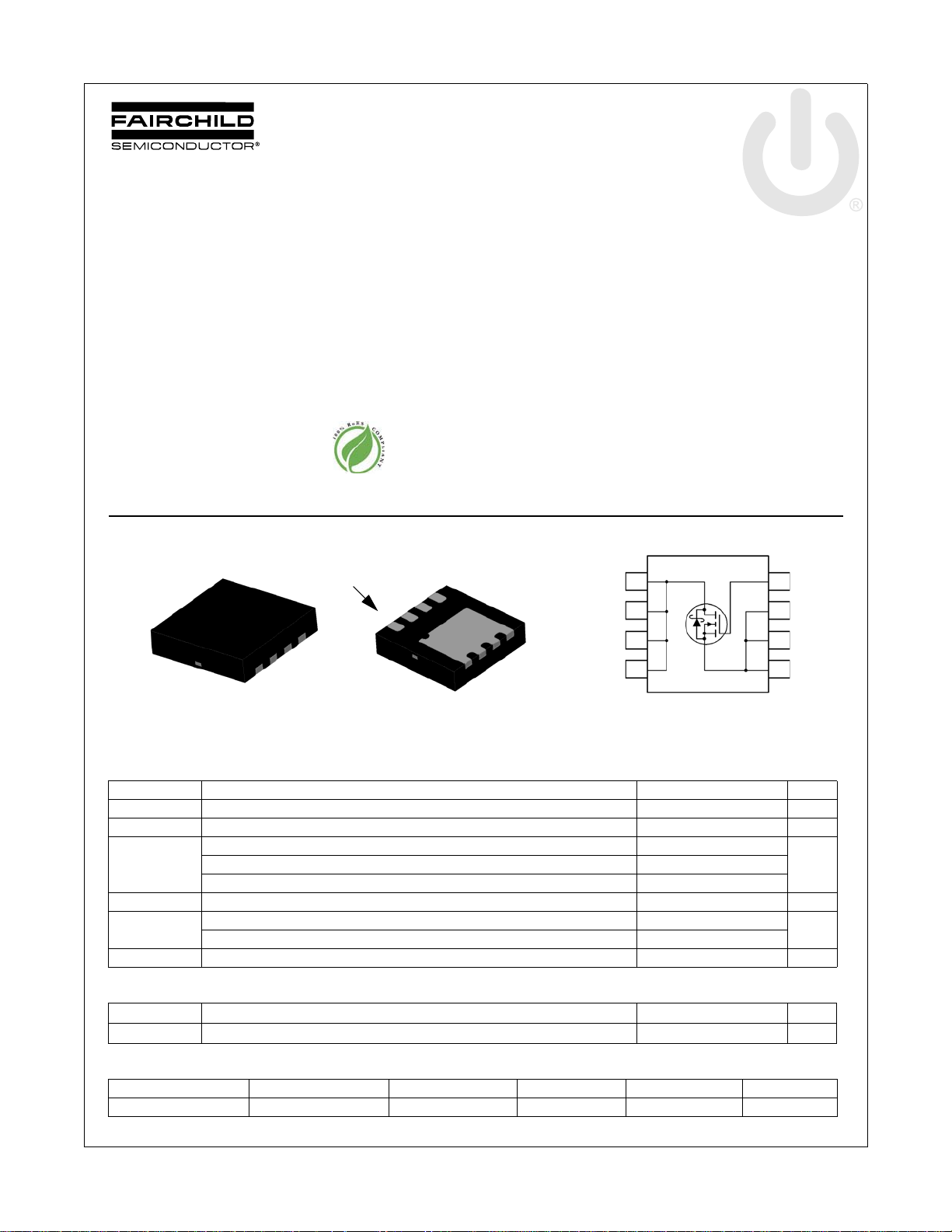
Top
Pin 1
S
Bottom
D
G
S
S
D
D
D
D
5
D
6
D
7
8
D
MLP 3.3x3.3
MOSFET Maximum Ratings T
Symbol Parameter Ratings Units
V
DS
V
GS
I
D
E
AS
P
D
, T
T
J
STG
Drain to Source Voltage 30 V
Gate to Source Voltage ±20 V
Drain Current -Continuous (Package limited) TC= 25 °C 18
-Pulsed 45
Single Pulse Avalanche Energy (Note 3) 60 mJ
Power Dissipation TC = 25 °C 36
Power Dissipation T
Operating and Storage Junction Temperature Range -55 to +150 °C
= 25 °C unless otherwise noted
A
= 25 °C (Note 1a) 14.8
A
= 25 °C (Note 1a) 2.3
A
Thermal Characteristics
®
SyncFET
TM
G
4
S
3
S
2
S
1
A -Continuous T
W
R
TJC
R
TJA
Thermal Resistance, Junction to Case 3.5 °C/W
Thermal Resistance, Junction to Ambient (Note 1a) 53 °C/W
Package Marking and Ordering Information
Device Marking Device Package Reel Size Tape Width Quantity
FDMC7672S FDMC7672S MLP 3.3X3.3 13 ’’ 12 mm 3000 units
©2010 Fairchild Semiconductor Corporation
FDMC7672S Rev.C3
1
www.fairchildsemi.com
Page 2
Electrical Characteristics T
Symbol Parameter Test Conditions Min Typ Max Units
= 25 °C unless otherwise noted
J
Off Characteristics
BV
'BV
'T
I
DSS
I
GSS
DSS
DSS
J
Drain to Source Breakdown Voltage ID = 1 mA, VGS = 0 V 30 V
Breakdown Voltage Temperature
Coefficient
Zero Gate Voltage Drain Current VDS = 24 V, V
Gate to Source Leakage Current VGS = 20 V, V
I
= 10 mA, referenced to 25 °C 12 mV/°C
D
= 0 V 1 mA
GS
= 0 V 100 nA
DS
FDMC7672S N-Channel Power Trench
On Characteristics
V
GS(th)
'V
'T
r
DS(on)
g
FS
GS(th)
J
Gate to Source Threshold Voltage VGS = VDS, ID = 1 mA 1.2 1.6 3.0 V
Gate to Source Threshold Voltage
Temperature Coefficient
Static Drain to Source On Resistance
Forward Transconductance VDS = 5 V, ID = 14.8 A 78 S
(Note 2)
Dynamic Characteristics
C
iss
C
oss
C
rss
R
g
Input Capacitance
Output Capacitance 770 1025 pF
Reverse Transfer Capacitance 85 130 pF
Gate Resistance 1.2 3.2 :
Switching Characteristics
t
d(on)
t
r
t
d(off)
t
f
Q
Q
Q
Q
g
g
gs
gd
Turn-On Delay Time
Rise Time 410ns
Turn-Off Delay Time 26 42 ns
Fall Time 310ns
Total Gate Charge VGS = 0 V to 10 V
Total Gate Charge VGS = 0 V to 4.5 V 14 20 nC
Gate to Source Gate Charge 5.3 nC
Gate to Drain “Miller” Charge 4.0 nC
= 10 mA, referenced to 25 °C -6 mV/°C
I
D
V
= 10 V, ID = 14.8 A 5.0 6.0
GS
= 4.5 V, ID = 12.4 A 6.1 7.1
V
GS
= 10 V, ID = 14.8 A
V
GS
= 125 °C
T
J
= 15 V, VGS = 0 V,
V
DS
5.9 9.0
1895 2520 pF
f = 1 MHz
11 21 n s
= 15 V, ID = 14.8 A,
V
DD
V
= 10 V, R
GS
GEN
= 6 :
30 42 nC
= 15 V
V
DD
I
= 14.8 A
D
m:
®
SyncFET
TM
Drain-Source Diode Characteristics
V
SD
t
rr
Q
rr
Notes:
1. R
TJA
the user's board design.
2. Pulse Test: Pulse Width < 300 Ps, Duty cycle < 2.0%.
of 60 mJ is based on starting TJ = 25 °C, L = 1 mH, IAS = 11 A, VDD = 27 V, VGS = 10 V. 100% test at L = 3 mH, IAS = 4.8 A.
3. E
AS
©2010 Fairchild Semiconductor Corporation
FDMC7672S Rev.C3
Source to Drain Diode Forward Voltage
Reverse Recovery Time
Reverse Recovery Charge 28 44 nC
is determined with the device mounted on a 1in2 pad 2 oz copper pad on a 1.5 x 1.5 in. board of FR-4 material. R
V
= 0 V, IS= 14.8 A (Note 2) 0.8 1.3
GS
= 0 V, IS= 1.9 A (Note 2) 0.5 1.2
V
GS
= 14.8 A, di/dt = 300 A/Ps
I
F
a. 53 °C/W when mounted on a
1 in2pad of 2 oz copper.
V
29 45 ns
is guaranteed by design while R
TJC
b. 125 °C/W when mounted on a
minimum pad of 2 oz copper.
2
is determined by
TCA
www.fairchildsemi.com
Page 3
FDMC7672S N-Channel Power Trench
Typical Characteristics T
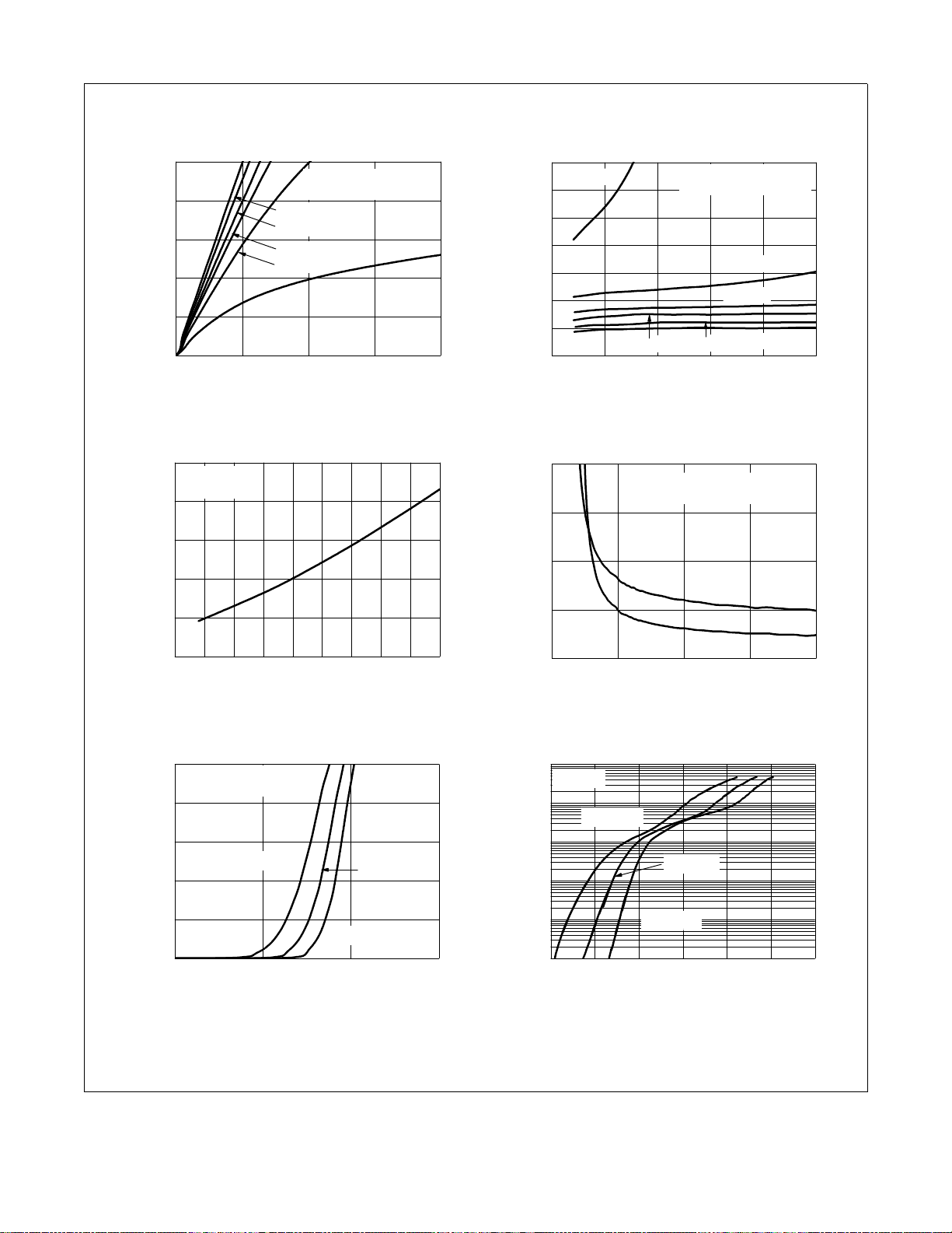
45
VGS = 10 V
36
27
18
DRAIN CURRENT (A)
,
9
D
I
0
0 0.2 0.4 0.6 0.8
V
DRAIN TO SOURCE VOLTAGE (V)
,
DS
Figure 1.
1.6
1.4
On-Region Characteristics
ID = 14.8 A
V
= 10 V
GS
1.2
1.0
NORMALIZED
0.8
DRAIN TO SOURCE ON-RESISTANCE
0.6
-75 -50 -25 0 25 50 75 100 125 150
T
JUNCTION TEMPERATURE
,
J
F i g u r e 3 . N o r m a l i z e d O n - R e s i s t a n c e
vs Junction Temperature
PULSE DURATION = 80 Ps
DUTY CYCLE = 0.5% MAX
VGS = 6 V
VGS = 4.5 V
VGS = 4 V
VGS = 3.5 V
= 25 °C unless otherwise noted
J
VGS = 3 V
o
(
C
)
4.0
VGS = 3 V
3.5
PULSE DURATION = 80 Ps
DUTY CYCLE = 0.5% MAX
3.0
2.5
VGS = 6 V
VGS = 3.5 V
V
=4 V
GS
V
GS
=10 V
2.0
NORMALIZED
1.5
1.0
DRAIN TO SOURCE ON-RESISTANCE
0.5
0 9 18 27 36 45
Figure 2.
VGS = 4.5 V
,
DRAIN CURRENT (A)
I
D
N o r m a l i z e d O n - R e s i s t a n c e
vs Drain Current and Gate Voltage
15
)
:
m
(
12
9
DRAIN TO
,
DS(on)
r
6
SOURCE ON-RESISTANCE
3
246810
Figure 4.
ID= 14.8 A
V
GATE TO SOURCE VOLTAGE (V)
,
GS
O n - R es i s t a n c e vs G a t e t o
PULSE DURATION = 80 Ps
DUTY CYCLE = 0.5% MAX
TJ= 125 oC
TJ= 25 oC
Source Voltage
®
SyncFET
TM
45
PULSE DURATION = 80 Ps
DUTY CYCLE = 0.5% MAX
36
VDS= 5 V
27
TJ = 125 oC
18
, DRAIN CURRENT (A)
D
I
9
0
1234
VGS, GATE TO SOURCE VOLTAGE (V)
Figure 5. Transfer Characteristics
©2010 Fairchild Semiconductor Corporation
FDMC7672S Rev.C3
TJ = 25 oC
TJ = -55 oC
100
VGS= 0 V
10
TJ= 125 oC
1
TJ = 25 oC
0.1
0.01
, REVERSE DRAIN CURRENT (A)
S
I
0.001
0.0 0.2 0.4 0.6 0.8 1.0 1.2
VSD, BODY DIODE FORWARD VOLTAGE (V)
Figure 6.
TJ = -55 oC
S o u r ce t o D r a i n Di o d e
Forward Voltage vs Source Current
3
www.fairchildsemi.com
Page 4

FDMC7672S N-Channel Power Trench
Typical Characteristics T
10
ID= 14.8 A
8
6
VDD = 15 V
4
2
, GATE TO SOURCE VOLTAGE (V)
GS
V
0
0 4 8 121620242832
Qg, GATE CHARGE (nC)
Figure 7.
Gate Charge Characteristics Figure 8.
40
10
TJ= 125 oC
, AVALANCHE CURRENT (A)
AS
I
1
0.01 0.1 1 10 100
tAV, TIME IN AVALANCHE (ms)
VDD= 10 V
VDD = 20 V
TJ= 25 oC
= 25 °C unless otherwise noted
J
TJ= 100 oC
5000
1000
100
CAPACITANCE (pF)
f = 1 MHz
= 0 V
V
GS
10
0.1 1 10
VDS, DRAIN TO SOURCE VOLTAGE (V)
C a p a c i t a n c e v s D r a i n
to Source Voltage
100
10
1
THIS AREA IS
LIMITED BY r
, DRAIN CURRENT (A)
D
I
SINGLE PULSE
0.1
0.01
= MAX RATED
T
J
R
T
JA
T
= 25 oC
A
0.01 0.1 1 10 100
DS(on)
= 125 oC/W
VDS, DRAIN to SOURCE VOLTAGE (V)
C
C
C
iss
oss
rss
30
®
SyncFET
100 us
TM
1ms
10 ms
100 ms
1 s
10 s
DC
Figure 9.
U n c l a m p e d I n d u c t i v e
Switching Capability
2000
1000
100
10
, PEAK TRANSIENT POWER (W)
(PK)
1
P
0.5
-4
10
©2010 Fairchild Semiconductor Corporation
FDMC7672S Rev.C3
-3
10
Figure 10.
F or w ar d Bi a s S a fe
Operating Area
-2
10
-1
10
t, PULSE WIDTH (sec)
110
Figure 11. Single Pulse Maximum Power Dissipation
4
VGS = 10V
SINGLE PULSE
= 125 oC/W
R
JA
T
T
= 25 oC
A
100 1000
www.fairchildsemi.com
Page 5

FDMC7672S N-Channel Power Trench
Typical Characteristics T
2
1
DUTY CYCLE-DESCENDING ORDER
D = 0.5
0.2
0.1
0.05
0.02
0.01
-4
10
-3
10
Figure 12. Junction-to-Ambient Transient Thermal Response Curve
NORMALIZED THERMAL
JA
T
0.01
IMPEDANCE, Z
0.001
0.0001
0.1
= 25 °C unless otherwise noted
J
SINGLE PULSE
R
= 125 oC/W
JA
T
-2
10
t, RECTANGULAR PULSE DURATION (sec)
-1
10
P
DM
NOTES:
DUTY FACTOR: D = t1/t
PEAK TJ = PDM x Z
TJA
110
t
1
t
2
2
x R
+ T
TJA
A
100 1000
®
SyncFET
TM
©2010 Fairchild Semiconductor Corporation
FDMC7672S Rev.C3
5
www.fairchildsemi.com
Page 6

Typical Characteristics (continued)
SyncFET Schottky body diode
Characteristics
FDMC7672S N-Channel Power Trench
Fairchild’s SyncFET process embeds a Schottky diode in parallel
with PowerTrench MoSFET. This diode exhibits similar
characteristics to a discrete external Schottky diode in parallel
with a MOSFET. Figure 13 shows the reverses recovery
characteristic of the FDMC7672S.
20
15
didt = 300 A/Ps
10
5
CURRENT (A)
0
-5
0 40 80 120 160 200
TIME (ns)
Figure 13. SyncFET body diode reverse
recovery characteristic
Schottky barrier diodes exhibit significant leakage at high temperature and high reverse voltage. This will increase the power
in the device.
-2
10
TJ= 125 oC
-3
10
-4
10
-5
10
, REVERSE LEAKAGE CURRENT (A)
-6
10
DSS
I
0 5 10 15 20 25 30
TJ= 100 oC
TJ= 25 oC
VDS, REVERSE VOLTAGE (V)
Figure 14. SyncFET body diode reverses
leakage versus drain-source voltage
®
SyncFET
TM
©2010 Fairchild Semiconductor Corporation
FDMC7672S Rev.C3
6
www.fairchildsemi.com
Page 7

Dimensional Outline and Pad Layout
FDMC7672S N-Channel Power Trench
®
SyncFET
TM
©2010 Fairchild Semiconductor Corporation
FDMC7672S Rev.C3
7
www.fairchildsemi.com
Page 8

TRADEMARKS
The following includes registered and unregistered trademarks and service marks, owned by Fairchild Semiconductor and/or its global subsidiaries, and is not
intended to be an exhaustive list of all such trademarks.
AccuPower™
Auto-SPM™
Build it Now™
CorePLUS™
CorePOWER™
CROSSVOLT™
CTL™
Current Transfer Logic™
DEUXPEED
Dual Cool™
EcoSPARK
®
®
EfficientMax™
ESBC™
®
®
Fairchild
Fairchild Semiconductor
FACT Quiet Series™
®
FACT
®
FAST
FastvCore™
FETBench™
FlashWriter
®
*
FPS™
®
F-PFS™
FRFET
Global Power ResourceSM
Green FPS™
Green FPS™ e-Series™
Gmax™
GTO™
IntelliMAX™
ISOPLANAR™
MegaBuck™
MICROCOUPLER™
MicroFET™
MicroPak™
MicroPak2™
MillerDrive™
MotionMax™
Motion-SPM™
OptoHiT™
OPTOLOGIC
OPTOPLANAR
PDP SPM™
®
Power-SPM™
PowerTrench
®
PowerXS™
Programmable Active Droop™
®
QFET
QS™
Quiet Series™
RapidConfigure™
™
Saving our world, 1mW/W/kW at a time™
SignalWise™
SmartMax™
SMART START™
®
SPM
STEALTH™
SuperFET™
SuperSOT™-3
®
®
®
SuperSOT™-6
SuperSOT™-8
SupreMOS™
SyncFET™
Sync-Lock™
* Trademarks of System General Corporation, used under license by Fairchild Semiconductor.
The Power Franchise
TinyBoost™
TinyBuck™
TinyCalc™
TinyLogic
TINYOPTO™
TinyPower™
TinyPWM™
TinyWire™
TriFault Detect™
TRUECURRENT™*
μSerDes™
UHC
Ultra FRFET™
UniFET™
VCX™
VisualMax™
XS™
®
*
®
®
FDMC7672S N-Channel Power Trench
®
®
SyncFET
TM
DISCLAIMER
FAIRCHILD SEMI CONDUCTOR RESERVES THE RIGH T TO MAKE CHANGES WITHOUT FURTHER NOTICE TO ANY PRODUCTS HEREI N TO IM PROVE
RELIABILITY, FUNCTION, OR DESI GN. FAI RCHILD DO ES NOT ASSUME ANY LI ABILI TY ARISI NG OUT OF THE APPLI CATION OR USE O F ANY PRODUCT OR
CIRCUIT DESCRIBED HEREIN; NEI THER DOES IT CONVEY ANY LICENSE UNDER I TS PATENT RIGHTS, NOR THE RI GHTS OF OTHERS. THESE
SPECIFICATIONS DO NOT EX PAND THE TERMS OF FAIRCHI LD’S WORLDWIDE TERMS AND CONDITIONS, SPECIF ICALLY THE WARRANTY THEREIN,
WHICH COVERS THESE PRODUCTS.
LIFE SUPPORT POLICY
FAIRCHILD’S PRODUCTS ARE NOT AUTHORIZED FOR USE AS CRI TICAL COM PONENTS IN L IFE SUPPORT DEVI CES OR SYSTEM S WITHOUT THE
EXPRESS WRITTEN APPROVAL OF FAIRCHILD SEM I CONDUCTOR CORPORATI ON.
As used herein:
1. Li fe support devices or systems are devices or systems which, (a) are
intended for surgical implant into the body or (b) support or sustain life,
and (c) whose failure to perform when properly used in accordance
with instructions for use provided in the labeling, can be reasonably
expected to result in a significant injury of the user.
2. A critical component in any component of a life support, device, or
system whose failure to perform can be reasonably expected to
cause the failure of the life support device or system, or to affect its
safety or effectiveness.
ANTI-COUNTERFEITING POLICY
Fairchild Semiconductor Corporation's Anti-Counterfeiting Policy. Fairchild's Anti-Counterfeiting Policy is also stated on our external website, www.fairchildsemi.com,
under Sales Support.
Counterfeiting of semiconductor parts is a growing problem in the industry. All manufacturers of semiconductor products are experiencing counterfeiting of their parts.
Customers who inadvertently purchase counterfeit parts experience many problems such as loss of brand reputation, substandard performance, failed applications,
and increased cost of production and manufacturing delays. Fairchild is taking strong measures to protect ourselves and our customers from the proliferation of
counterfeit parts. Fairchild strongly encourages customers to purchase Fairchild parts either directly from Fairchild or from Authorized Fairchild Distributors who are
listed by country on our web page cited above. Products customers buy either from Fairchild directly or from Authorized Fairchild Distributors are genuine parts, have
full traceability, meet Fairchild's quality standards for handling and storage and provide access to Fairchild's full range of up-to-date technical and product information.
Fairchild and our Authorized Distributors will stand behind all warranties and will appropriately address any w arranty issues that may arise. Fairchild w ill not pro vide
any warranty coverage or other assistance for parts bought from Unauthorized Sources. Fairchild is committed to combat this global problem and encourage our
customers to do their part in stopping this practice by buying direct or from authorized distributors.
PRODUCT STATUS DEFINITIONS
Definition of Terms
Datasheet Identification Product Status Definition
Advance Information Formative / In Design
Preliminary First Production
No Identification Needed Full Production
Obsolete Not In Production
©2010 Fairchild Semiconductor Corporation
FDMC7672S Rev.C3
Datasheet contains the design specifications for product development. Specifications may change in
any manner without notice.
Datasheet contains preliminary data; supplementary data will be published at a later date. Fairchild
Semiconductor reserves the right to make changes at any time without notice to improve design.
Datasheet contains final specifications. Fairchild Semiconductor reserves the right to make changes
at any time without notice to improve the design.
Datasheet contains specifications on a product that is discontinued by Fairchild Semiconductor.
The datasheet is for reference information only.
8
www.fairchildsemi.com
Rev. I48
 Loading...