

Page 1
FDMC510P
P-Channel PowerTrench® MOSFET
-20 V, -18 A, 8.0 mΩ
Features
Max r
Max r
Max r
Max r
High performance trench technology for extremely low r
High power and current handling capability in a widely used
surface mount package
100% UIL Tested
Termination is Lead-free and RoHS Compliant
HBM ESD capability level >2 KV typical (Note 4)
= 8.0 mΩ at VGS = -4.5 V, ID = -12 A
DS(on)
= 9.8 mΩ at VGS = -2.5 V, ID = -10 A
DS(on)
= 13 mΩ at VGS = -1.8 V, ID = -9.3 A
DS(on)
= 17 mΩ at VGS = -1.5 V, ID = -8.3 A
DS(on)
DS(on)
General Description
This P-Channel MOSFET is produced using Fairchild
Semiconductor’s advanced Power Trench
been
optimized for r
ruggedness.
Applications
Battery Management
Load Switch
®
, switching performance and
DS(ON)
process that has
FDMC510P P-Channel PowerTrench
June 2010
®
MOSFET
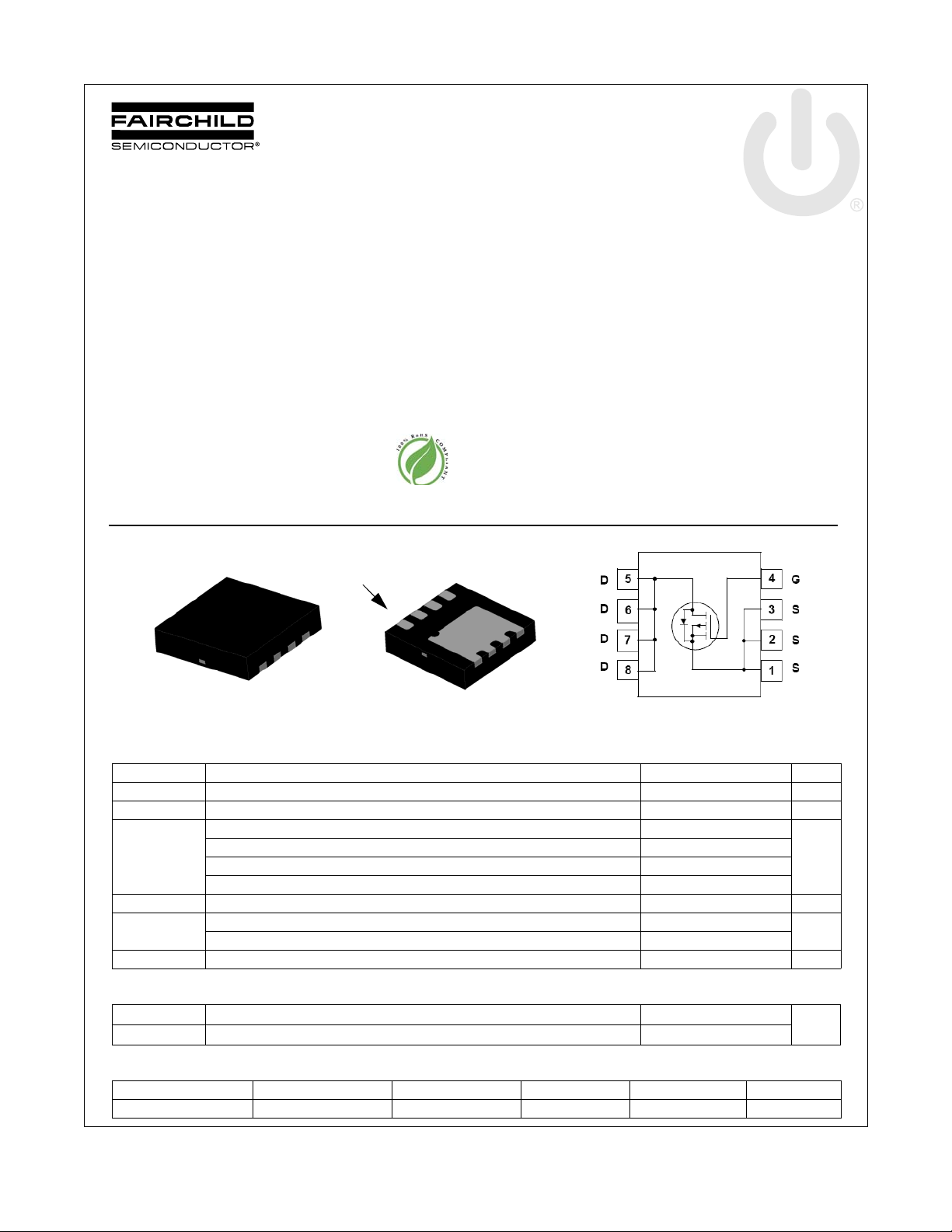
Top
Pin 1
S
Bottom
G
S
S
D
D
D
D
MLP 3.3x3.3
MOSFET Maximum Ratings T
Symbol Parameter Ratings Units
V
DS
V
GS
I
D
E
AS
P
D
, T
T
J
STG
Drain to Source Voltage -20 V
Gate to Source Voltage ±8 V
Drain Current -Continuous (Package limited) TC = 25 °C -18
-Continuous (Silicon limited) T
-Continuous T
-Pulsed -50
Single Pulse Avalanche Energy 37 mJ
Power Dissipation TC = 25 °C 41
Power Dissipation T
Operating and Storage Junction Temperature Range -55 to +150 °C
= 25 °C unless otherwise noted
A
= 25 °C -54
C
= 25 °C (Note 1a) -12
A
= 25 °C (Note 1a) 2.3
A
Thermal Characteristics
A
W
R
θJC
R
θJA
Thermal Resistance, Junction to Case 3
Thermal Resistance, Junction to Ambient (Note 1a) 53
Package Marking and Ordering Information
Device Marking Device Package Reel Size Tape Width Quantity
FDMC510P FDMC510P MLP 3.3X3.3 13 ’’ 12 mm 3000 units
©2010 Fairchild Semiconductor Corporation
FDMC510P Rev.C5
°C/W
1
www.fairchildsemi.com
Page 2
FDMC510P P-Channel PowerTrench
Electrical Characteristics T
= 25 °C unless otherwise noted
J
Symbol Parameter Test Conditions Min Typ Max Units
Off Characteristics
BV
∆BV
∆T
I
DSS
I
GSS
DSS
DSS
J
Drain to Source Breakdown Voltage ID = -250 µA, VGS = 0 V -20 V
Breakdown Voltage Temperature
Coefficient
Zero Gate Voltage Drain Current VDS = -16 V, V
Gate to Source Leakage Current VGS = ±8 V, V
I
= -250 µA, referenced to 25 °C -12 mV/°C
D
= 0 V -1 µA
GS
= 0 V ±100 nA
DS
On Characteristics
V
GS(th)
∆V
∆T
r
DS(on)
g
FS
GS(th)
J
Gate to Source Threshold Voltage VGS = VDS, ID = -250 µA -0.4 -0.5 -1.0 V
Gate to Source Threshold Voltage
Temperature Coefficient
Static Drain to Source On Resistance
I
= -250 µA, referenced to 25 °C 3 mV/°C
D
= -4.5 V, ID = -12 A 6.4 8.0
V
GS
V
= -2.5 V, ID = -10 A 7.6 9.8
GS
= -1.8 V, ID = -9.3 A 9.2 13
V
GS
= -1.5 V, ID = -8.3 A 11 17
V
GS
= -4.5 V, ID = -12 A, TJ = 125 °C 8.5 12
V
GS
Forward Transconductance VDS = -5 V, ID = -12 A 75 S
Dynamic Characteristics
C
iss
C
oss
C
rss
Input Capacitance
Output Capacitance 840 1120 pF
Reverse Transfer Capacitance 738 1110 pF
= -10 V, VGS = 0 V,
V
DS
f = 1 MHz
5910 7860 pF
mΩ
®
MOSFET
Switching Characteristics
t
d(on)
t
r
t
d(off)
t
f
Q
g(TOT)
Q
g(TOT)
Q
gs
Q
gd
Turn-On Delay Time
Rise Time 34 55 ns
Turn-Off Delay Time 338 540 ns
Fall Time 170 272 ns
Total Gate Charge VGS = 0 V to -4.5 V
Total Gate Charge VGS = 0 V to -2.5 V 50 70 nC
Gate to Source Charge 6.3 nC
Gate to Drain “Miller” Charge 20.4 nC
= -10 V, ID = -12 A,
V
DD
V
= -4.5 V, R
GS
GEN
= 6 Ω
Drain-Source Diode Characteristics
V
= 0 V, IS = -12 A (Note 2) -0.70 -1.3
V
SD
t
rr
Q
rr
Notes:
1: R
θJA
by the user’s board design.
Source to Drain Diode Forward Voltage
Reverse Recovery Time
Reverse Recovery Charge 20 32 nC
is determined with the device mounted on a 1 in2 pad 2 oz copper pad on a 1.5 x 1.5 in. board of FR-4 material. R
a. 53 °C/W when mounted on
a 1 in2 pad of 2 oz c o p p e r
GS
= 0 V, IS = -2 A (Note 2) -0.53 -1.2
V
GS
= -12 A, di/dt = 100 A/µs
I
F
= -10 V,
V
DD
I
= -12 A
D
15 27 ns
83 116 nC
35 57 ns
is guaranteed by design while R
θJC
b. 125 °C/W when mounted on a
minimum pad of 2 oz copper
V
is determined
θJA
2: Pulse Test: Pulse Width < 300 µs, Duty cycle < 2.0%.
3: Starting T
4: No gate overvoltage rating is implied.
FDMC510P Rev.C5
= 25oC; P-Ch: L = 3 mH, IAS = -5 A, VDD = -20 V, VGS = -4.5 V.
J
2
www.fairchildsemi.com
Page 3
FDMC510P P-Channel PowerTrench
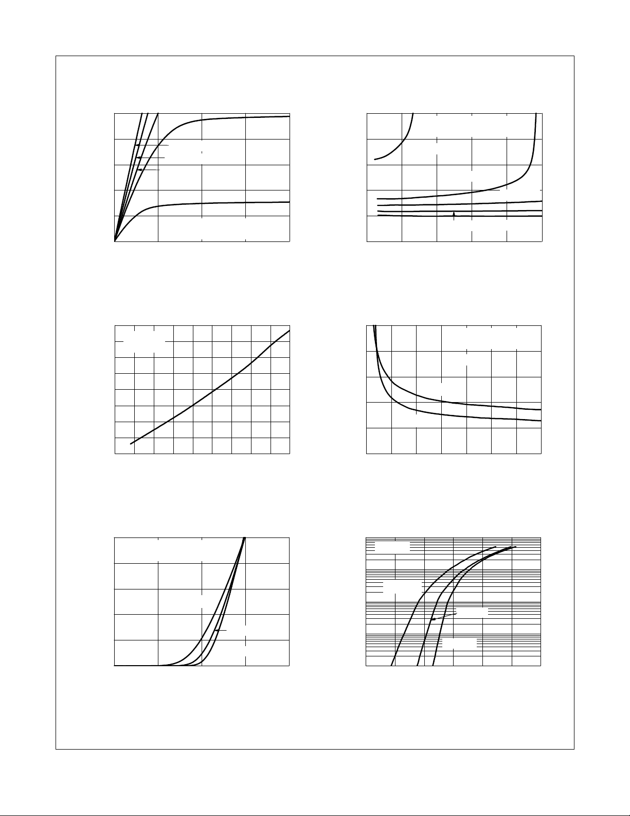
Typical Characteristics T
50
40
30
20
DRAIN CURRENT (A)
,
D
10
-I
0
0.0 0.5 1.0 1.5 2.0
Figure 1.
1.5
ID = -12 A
NORMALIZED
DRAIN TO SOURCE ON-RESISTANCE
1.4
1.3
1.2
1.1
1.0
0.9
0.8
0.7
= -4.5 V
V
GS
-75 -50 -25 0 25 50 75 100 125 150
VGS = -4.5 V
VGS = -2.5 V
VGS = -1.8 V
PULSE DURATION = 80 µs
DUTY CYCLE = 0.5%MAX
-V
,
DRAIN TO SOURCE VOLTAGE (V)
DS
On Region Characteristics Figure 2.
T
,
JUNCTION TEMPERATUR E
J
= 25 °C unless otherwise noted
J
VGS = - 1.5 V
VGS = -1.2 V
o
(
C
)
5
PULSE DURATION = 80 µs
4
DUTY CYCLE = 0.5%MAX
VGS = -1.2 V
3
2
NORMALIZED
VGS = -1.5 V
VGS = -1.8 V
1
V
= -2.5 V
DRAIN TO SOURCE ON-RESISTANCE
0
0 1020304050
-I
D
GS
,
DRAIN CURRENT (A)
V
GS
Normalized On-Resistance
vs Drain Current and Gate Voltage
25
)
Ω
20
m
(
15
10
, DRAIN TO
DS(on)
r
5
SOURCE ON-RESISTANCE
0
1.0 1.5 2.0 2.5 3.0 3.5 4.0 4.5
T
= 25 oC
J
-V
,
GATE TO S OURCE VO LTAGE (V
GS
PULSE DURATION = 80 µs
DUTY CYCLE = 0.5%MAX
ID = -12 A
TJ = 125 oC
)
= -4.5 V
®
MOSFET
Fi g ure 3 . Norma l i zed O n Resi s t ance
50
40
30
20
, DRAIN CURRENT (A)
D
10
-I
0
0.0 0.5 1.0 1.5 2.0
FDMC510P Rev.C5
vs Junction Temperature
PULSE DURATION = 80 µs
DUTY CYCLE = 0.5%MAX
V
= -5 V
DS
TJ = 150 oC
TJ = 25 oC
TJ = -55 oC
-VGS, GATE TO SOURCE VO LTAGE (V)
Figure 5. Transfer Characteristics
Figure 4.
On-Resi st an ce vs Gate to
Source Voltage
100
V
= 0 V
GS
10
TJ = 150 oC
1
TJ = 25 oC
0.1
, REVERSE DRAIN CURRENT (A)
S
-I
0.01
0.00.20.40.60.81.01.2
-VSD, BODY DIODE FORWARD VOLTAGE (V)
Figure 6.
Sou rc e t o D rain Di ode
TJ = -55 oC
Forward Voltage vs Source Current
3
www.fairchildsemi.com
Page 4

FDMC510P P-Channel PowerTrench
Typical Characteristics T
4.5
ID = -12 A
3.0
V
= -8 V
DD
1.5
, GATE TO SOURCE VOLTAGE (V)
GS
-V
0.0
020406080100
Figure 7.
Qg, GATE CHARGE (nC)
Gate Charge Characteristics Figure 8.
20
10
, AVALANCHE CURRENT (A)
AS
-I
1
0.1 1 10 100 1 000
tAV, TIME IN AVA LANCHE (m s )
VDD = -10 V
TJ = 125 oC
= 25 °C unless otherwise noted
J
VDD = -12 V
TJ = 25 oC
TJ = 100 oC
20000
10000
CAPACITANCE (pF)
1000
400
f = 1 MHz
= 0 V
V
GS
0.1 1 10 20
-VDS, DRAIN TO SOURCE VOLTA G E (V)
Capac i t a n c e vs Dr a i n
to Source Voltage
60
50
40
V
= -2.5 V
GS
30
20
, DRAIN CURRENT (A)
D
-I
10
Limited by Package
0
25 50 75 100 125 150
V
= -4.5 V
GS
R
= 3 oC/W
θJC
T
, CASE TEMPERATURE (
C
C
iss
C
oss
C
rss
®
MOSFET
o
C)
100
10
1
, DRAIN CURRENT (A)
0.1
D
-I
0.01
0.01 0.1 1 10 80
FDMC510P Rev.C5
Figure 9.
Un c l a m pe d I n du c t i ve
Switching Capability
100 us
1 ms
10 ms
THIS AREA IS
LIMITED BY r
DS(on)
SINGLE PULSE
= MAX RATED
T
J
R
= 125 oC/W
θ
JA
T
= 25 oC
A
-VDS, DRAIN TO SOURCE VOLTAGE (V)
100 ms
1 s
10 s
DC
Figure 11. Forward Bias Safe
Operating Area
Figure 10.
Ma ximum Con tin uou s Dr ain
Current vs Case Temperature
1000
100
SINGLE PULSE
R
T
θJA
A
= 25
= 125
o
o
C/W
C
10
), PEAK TRANSIENT POWER (W)
1
PK
P(
0.5
10-410-310-210
t, PULSE WIDTH (sec)
-1
110
100 1000
Figure 12. Single Pulse Maximum
Power Dissipation
4
www.fairchildsemi.com
Page 5

FDMC510P P-Channel PowerTrench
Typical Characteristics T
2
1
JA
θ
Z
0.1
IMPEDANCE,
0.01
NORMALIZED THERMAL
0.001
DUTY CYCLE-DESCENDING ORDER
D = 0.5
0.2
0.1
0.05
0.02
0.01
-4
10
-3
10
Figure 13.
= 25 °C unless otherwise noted
J
P
DM
SINGLE PULSE
R
= 125 oC/W
θ
JA
-2
10
t, RECTANGULAR PULSE DURATION (sec)
-1
10
110
NOTES:
DUTY FACTOR: D = t
PEAK TJ = PDM x Z
θJA
Junction-to-Ambient Transient Thermal Response Curve
t
1
t
2
1/t2
x R
+ T
θJA
A
100 1000
®
MOSFET
FDMC510P Rev.C5
5
www.fairchildsemi.com
Page 6

Dimensional Outline and Pad Layout
FDMC510P P-Channel PowerTrench
®
MOSFET
FDMC510P Rev.C5
6
www.fairchildsemi.com
Page 7

TRADEMARKS
tm
®
tm
tm
The following includes registered and unregistered trademarks and service marks, owned by Fairchild Semiconductor an d/or its global subsidiaries, and is not
intended to be an exhaustive list of all such trademarks.
AccuPower™
Auto-SPM™
Build it Now™
CorePLUS™
CorePOWER™
CROSSVOLT™
CTL™
Current Transfer Logic™
DEUXPEED
Dual Cool™
EcoSPARK
EfficentMax™
ESBC™
Fairchild
Fairchild Semiconductor
FACT Quiet Series™
FACT
FAST
FastvCore™
FETBench™
FlashWriter
®
®
®
®
®
®
*
FPS™
F-PFS™
®
FRFET
Global Power Resource
Green FPS™
Green FPS™ e-Series™
Gmax™
GTO™
IntelliMAX™
ISOPLANAR™
MegaBuck™
MICROCOUPLER™
MicroFET™
MicroPak™
MicroPak2™
MillerDrive™
®
MotionMax™
Motion-SPM™
OptiHiT™
OPTOLOGIC
OPTOPLANAR
®
®
SM
®
PDP SPM™
Power-SPM™
PowerTrench
PowerXS™
Programmable Active Droop™
QFET
QS™
Quiet Series™
RapidConfigure™
Saving our world, 1mW/W/kW at a time™
SignalWise™
SmartMax™
SMART START™
SPM
STEALTH™
SuperFET™
SuperSOT™-3
SuperSOT™-6
SuperSOT™-8
SupreMOS™
SyncFET™
®
®
™
®
Sync-Lock™
®*
The Power Franchise
TinyBoost™
TinyBuck™
TinyCalc™
TinyLogic
TINYOPTO™
TinyPower™
TinyPWM™
TinyWire™
TriFault Detect™
TRUECURRENT™*
µSerDes™
UHC
Ultra FRFET™
UniFET™
VCX™
VisualMax™
XS™
®
®
®
®
*Trademarks of System General Corporation, used under license by Fairchild Semiconductor.
DISCLAIMER
FAIRCHILD SEMICONDUCTOR RESERVES THE RIGHT TO MAKE CHANGES WITHOUT FURTHER NOTICE TO ANY PRODUCTS HEREIN TO IMPROVE
RELIABILITY, FUNCTION, OR DESIGN. FAIRCHILD DOES NOT ASSUME ANY LIABILITY ARISING OUT OF THE APPLICATION OR USE OF ANY
PRODUCT OR CIRCUIT DESCRIBED HEREIN; NEITHER DOES IT CONVEY ANY LICENSE UNDER ITS PATENT RIGHTS, NOR THE RIGHTS OF OTHERS.
THESE SPECIFICATIONS DO NOT EXPAND THE TERMS OF FAIRCHILD’S WORLDWIDE TERMS AND CONDITIONS, SPECIFICALLY THE WARRANTY
THEREIN, WHICH COVERS THESE PRODUCTS.
FDMC510P P-Channel PowerTrench
®
MOSFET
LIFE SUPPORT POLICY
FAIRCHILD’S PRODUCTS ARE NOT AUTHORIZED FOR USE AS CRITICAL COMPONENTS IN LIFE SUPPORT DEVICES OR SYSTEMS WITHOUT THE
EXPRESS WRITTEN APPROVAL OF FAIRCHILD SEMICONDUCTOR CORPORATION.
As used here in:
1. Life support devices or systems are devices or systems which, (a) are
intended for surgical implant into the body or (b) support or sustain life,
and (c) whose failure to perform when properly used in accordance with
instructions for use provided in the labeling, can be reasonably
expected to result in a significant injury of the user.
ANTI-COUNTERFEITING POLICY
Fairchild Semiconductor Corporation’s Anti-Counterfeiting Policy. Fairchild’s Anti-Counterfeiting Policy is also stated on our external website,
www.Fairchildsemi.com, under Sales Support
Counterfeiting of semiconductor parts is a growing problem in the industry. All manufactures of semiconductor products are experiencing counterfeiti ng of their
parts. Customers who inadvertently purchase counterfeit parts exper ience many problems such as l oss of bra nd reput at ion, su bsta n dard per fo rmance, f aile d
application, and increased cost of production and manufacturing delays. Fairchild is taking st rong measures to protect ourselves and our customers from the
proliferation of counterfeit parts. Fairchild str ongly encourages cust omers to purchase Fairchild parts either di rectly fro m Fairchild or from Aut horized Fairchild
Distributors who are listed by country on our web page cited above. Products customers buy either from Fairchild directly or from Authorized Fairchild
Distributors are genuine parts, have full traceability, meet Fai rchild’s quality standards for handing and storage and provide access to Fairchild’s full range of
up-to-date technical and product information. Fairchild and our Authorized Distributors will stand behind all warranties and will appropriately address and
warranty issues that may arise. Fairchild will not provide any warranty coverage or other assistance for parts bo ught from Unauthorized Sources. Fairchild is
committed to combat this global problem and encourage our customers to do their part in stopping th is practice by buying direct or from authorized distributors.
PRODUCT STATUS DEFINITIONS
Definition of Terms
.
2. A critical component in any component of a life support, device, or
system whose failure to perform can be reasonably expected to cause
the failure of the life support device or system, or to affect its safety or
effectiveness.
Datasheet Identification Product Status Definition
Advance Information Formative / In Design
Preliminary First Production
No Identification Needed Full Production
Obsolete Not In Production
Datasheet contains the design specifications for product development. Specifications
may change in any manner without notice.
Datasheet contains preliminary data; supplementary data will be published at a later
date. Fairchild Semiconductor reserves the right to make changes at any time without
notice to improve design.
Datasheet contains final specifications. Fairchild Semiconductor reserves the right to
make changes at any time without notice to improve the design.
Datasheet contains specifications on a product that is discontinued by Fairchild
Semiconductor. The datasheet is for reference information only.
Rev. I48
FDMC510P Rev.C5 7 www.fairchildsemi.com
 Loading...