

Page 1
tm
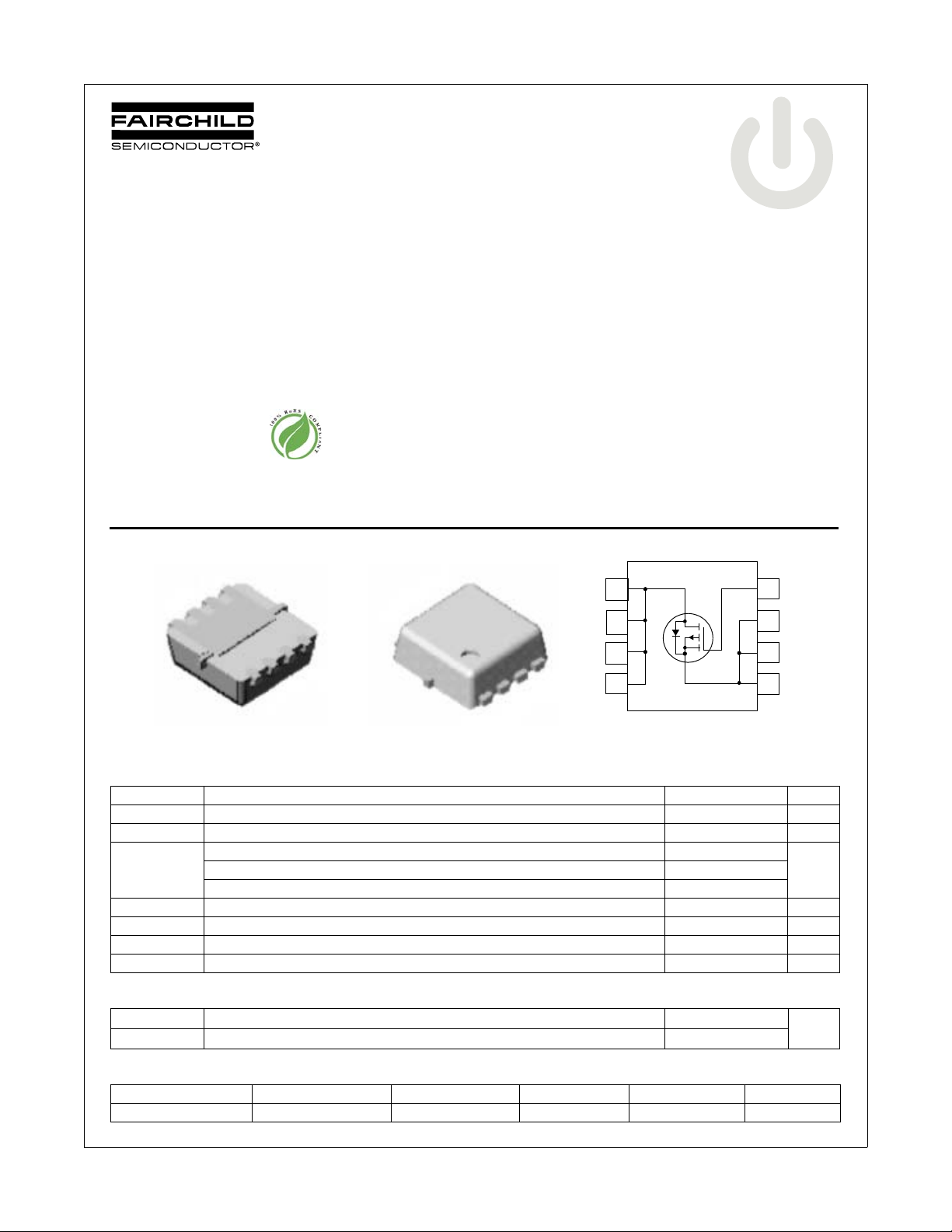
FDMC2523P
Power 33
S
S
S
G
D
D
D
D
8
1
7
2
3
4
6
5
1
2
3
4
5
6
7
8
D
D
D
D
G
S
S
S
Bottom
Top
P-Channel QFET®
-150V, -3A, 1.5Ω
Features
Max r
Low Crss ( typical 10pF)
Fast Switching
Low gate charge ( typical 6.2 nC )
Improved dv / dt capability
RoHS Compliant
= 1.5Ω at VGS = -10V, ID = -1.5A
DS(on)
General Description
These P-Channel MOSFET enhancement mode power field
effect transistors are produced using Fairchild's proprietary,
planar stripe, DMOS technology. This advanced technology has
been especially tailored to minimize on-state resistance, provide
superior switching performance, and withstand high energy
pulse in the avalanche and commutation mode. These devices
are well suited for low voltage applications such as audio
amplifier, high efficiency switching DC/DC converters, and DC
motor control.
Application
Active Clamp Switch
FDMC2523P P-Channel QFET
January 2007
®
MOSFET Maximum Ratings T
Symbol Parameter Ratings Units
V
DS
V
GS
I
D
P
D
, T
T
J
STG
T
L
dv/dt Peak Diode Recovery dv/dt (Note 2) -5 V/ns
Thermal Characteristics
R
θJC
R
θJA
Package Marking and Ordering Information
©2006 Fairchild Semiconductor Corporation
FDMC2523P Rev.C
Device Marking Device Package Reel Size Tape Width Quantity
FDMC2523P FDMC2523P Power 33 7’’ 8mm 3000 units
Drain to Source Voltage -150 V
Gate to Source Voltage ±30 V
Drain Current -Continuous TC = 25°C -3
-Pulsed -12
Power Dissipation (Steady State) TC = 25°C 42 W
Operating and Storage Junction Temperature Range -55 to +150 °C
Maximum lead temperature for soldering purposes, 1/8” from case for 5 seconds 300 °C
Thermal Resistance, Junction to Case (Note 1) 3.0
Thermal Resistance, Junction to Ambient (Note 1a) 60
= 25°C unless otherwise noted
A
= 100°C -1.8
C
A -Continuous T
°C/W
1
www.fairchildsemi.com
Page 2
FDMC2523P P-Channel QFET
Electrical Characteristics T
= 25°C unless otherwise noted
J
Symbol Parameter Test Conditions Min Typ Max Units
Off Characteristics
BV
ΔBV
ΔT
I
DSS
I
GSS
DSS
DSS
J
Drain to Source Breakdown Voltage ID = -250μA, VGS = 0V -150 V
Breakdown Voltage Temperature
Coefficient
Zero Gate Voltage Drain Current
Gate to Source Leakage Current VGS = ±30V, V
ID = -250μA, referenced to 25°C -138 mV/°C
VDS = -150V, VGS = 0V -1
TJ = 125°C -10
= 0V ±100 nA
DS
On Characteristics
V
GS(th)
ΔV
ΔT
r
DS(on)
g
FS
GS(th)
J
Gate to Source Threshold Voltage VGS = VDS, ID = -250μA -3 -3.8 -5 V
Gate to Source Threshold Voltage
Temperature Coefficient
Static Drain to Source On Resistance
ID = -250μA, referenced to 25°C 6 mV/°C
VGS = -10V, ID = -1.5A 1.1 1.5 Ω
VGS = -10V , ID = -1.5A , TJ = 125°C 2.0 3.6
Forward Transconductance VDS = -40V , ID = -1.5A (Note 4) 1.4 S
Dynamic Characteristics
C
iss
C
oss
C
rss
R
g
Input Capacitance
Output Capacitance 60 80 pF
Reverse Transfer Capacitance 10 15 pF
VDS = -25V, VGS = 0V,
f = 1MHz
200 270 pF
Gate Resistance f = 1MHz 7.5 Ω
Switching Characteristics
t
d(on)
t
r
t
d(off)
t
f
Q
Q
Q
g
gs
gd
Turn-On Delay Time
Rise Time 11 20 ns
Turn-Off Delay Time 19 35 ns
Fall Time 13 24 ns
Total Gate Charge V
Gate to Source Gate Charge 1.4 nC
Gate to Drain “Miller” Charge 3.3 nC
VDD = -75V, ID = -3A
VGS = -10V, R
= -10V
GS
VDD = -75V
GEN
= 25Ω
(Note 3,4)
ID = -3A
(Note 3,4)
15 27 ns
6.2 9 nC
μA
®
Drain-Source Diode Characteristics
I
S
I
SM
V
SD
t
rr
Q
rr
Notes:
1: R
θJA
R
is guaranteed by design while R
θJC
2: ISD < -3A, dI/dt < 300A/us, VDD < B
3: Pulse Test: Pulse Width < 300μs, Duty cycle < 2.0%.
4: Essentially independent of operating temperature.
FDMC2523P Rev.C
Maximum continuous Drain - Source Diode Forward Current -3 A
Maximum Pulse Drain - Source Doide Forward Current -12 A
Source to Drain Diode Forward Voltage V
Reverse Recovery Time
Reverse Recovery Charge 0.27 nC
is the sum of the junction-to-case and case-to- ambien t thermal resistan ce wher e the case the rmal r efere nce is de fined as the sold er moun ting su rfac e of the dr ain pi ns.
is determined by the user's board design.
θCA
, Starting TJ = 25°C
VDSS
GS
IF = -3.0A, di/dt = 100A/μs
(Note 3)
a. 60°C/W when mounted on
a 1 in2 pad of 2 oz copper
= 0V, IS = -3.0A -1.8 -5 V
93 ns
b.135°C/W when mounted on a
minimum pad of 2 oz copper
2
www.fairchildsemi.com
Page 3
FDMC2523P P-Channel QFET
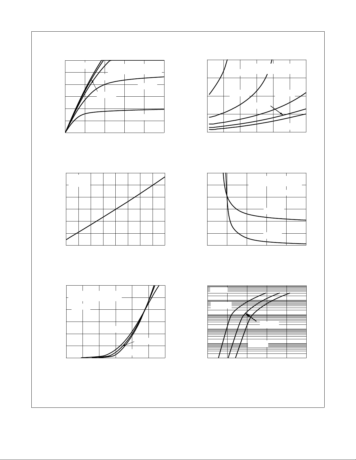
0246810
0.0
0.5
1.0
1.5
2.0
2.5
3.0
VGS = -8V
VGS = -9V
VGS = -6V
VGS = -7V
VGS = -10V
PULSE DURATION = 300μs
DUTY CYCLE = 2.0%MAX
-VDS, DRAIN TO SOURCE VOLTA GE (V)
- I
D
, DRAIN CURRENT (A)
0.0 0.5 1.0 1.5 2.0 2.5 3.0
0.8
1.0
1.2
1.4
1.6
V
GS
= -9V
V
GS
= -8V
V
GS
= -10V
V
GS
= -7V
PULSE DURATION = 300μs
DUTY CYCLE = 2.0%MAX
V
GS
= -6V
-ID, DRAIN CURRENT(A)
NORMALIZED
DRAIN TO SOURCE ON-RESISTANCE
-50 -25 0 25 50 75 100 125 150
0.3
0.6
0.9
1.2
1.5
1.8
2.1
ID = -3A
V
GS
= -10V
NORMALIZED
DRAIN TO SOURCE ON-RESISTANCE
TJ, JUNCTION TEMPERATURE (oC)
5678910
1.0
1.5
2.0
2.5
3.0
3.5
4.0
PULSE DURATION = 300μs
DUTY CYCLE = 2.0%MAX
TJ = 125oC
T
J
= 25
o
C
ID = -0.75A
r
DS(on)
, DRAIN TO
SOURCE ON-RESISTANCE
(Ω)
-VGS, GATE TO SOURCE VOLTAGE (V)
2345678
0.0
0.5
1.0
1.5
2.0
2.5
3.0
V
DD
= -5V
PULSE DURATION = 300μs
DUTY CYCLE = 2.0%MAX
TJ = -55oC
TJ = 25oC
TJ = 125oC
- I
D
, DRAIN CURRENT (A)
-VGS, GATE TO SOURCE VOLTAGE (V)
0.0 0.5 1.0 1.5 2.0 2.5
1E-4
1E-3
0.01
0.1
1
10
TJ = -55oC
TJ = 25oC
TJ = 125oC
V
GS
= 0V
- I
S
, REVERSE DRAIN CURRENT (A)
-VSD, BODY DIODE FORWA R D V OL TAGE (V)
Typical Characteristics T
Figure 1. On-Region Characteristics Figure 2. No rmali zed On -Resi stanc e
= 25°C unless otherwise noted
J
®
vs Drain Current and Gate Voltage
Figure 3 . N or maliz ed On - Resist an ce
vs Junction Temperature
FDMC2523P Rev.C
Figure 5. Transfer Characteristics Figure 6. Sou rce to Drain Diode
Figure 4. On-Resistance v s Gate to
Source Voltage
Forward Voltage vs Source Current
3
www.fairchildsemi.com
Page 4

FDMC2523P P-Channel QFET
02468
0
2
4
6
8
10
ID = -3A
VDD = -75V
VDD = -100V
VDD = -50V
-V
GS
, GATE TO SOURCE VOLTAGE(V)
Qg, GATE CHARGE(nC)
0 25 50 75 100 125 150
1
10
100
1000
C
iss
f = 1MHz
V
GS
= 0V
CAPACITANCE (pF)
-VDS, DRAIN TO SOURCE VOLTAGE (V)
C
rss
C
oss
10
-2
10
-1
10
0
10
1
1
6
0.5
20
TJ = 125oC
TJ = 25oC
I
AS
, AVALANCHE CURRENT(A)
tAV, TIME IN AVALANCHE(μs)
110100
1E-3
0.01
0.1
1
10
10s
100us
1ms
10ms
100ms
1s
DC
I
D
, DRAIN CURRENT (A)
VDS, DRAIN to SOURCE VOLTAGE (V)
40
SINGLE PULSE
T
J
= MAX RATED
R
θJA
= 135oC/W
T
A
= 25oC
400
r
DS(on)
LIMITED
10
-4
10
-3
10
-2
10
-1
10
0
10
1
10
2
10
3
1
10
100
SINGLE PULSE
R
θJA
= 135oC/W
0.5
P(
PK
), PEAK TRANSIENT POWER (W)
t, PULSE WIDTH (s)
500
TA = 25oC
I = I
25
FOR TEMPERATURES
ABOVE 25oC DERATE PEAK
CURRENT AS FOLLOWS:
150 T
A
–
125
----------------------- -
Typical Characteristics T
Figure 7. Gate Charge Characteristics Figure 8. Cap aci tan ce vs D rai n
= 25°C unless otherwise noted
J
®
to Source Voltage
Figure 9. U ncl amp ed I ndu c tiv e
Switching Capability
FDMC2523P Rev.C
Figure 11. Single Pulse Maximum Power Dissipation
Figure 10. Forward Bi as Safe
Operating Area
4
www.fairchildsemi.com
Page 5

FDMC2523P P-Channel QFET
10
-4
10
-3
10
-2
10
-1
10
0
10
1
10
2
10
3
1E-3
0.01
0.1
1
SINGLE PULSE
R
θJA
= 135oC/W
D = 0.5
0.2
0.1
0.05
0.02
0.01
DUTY CYCLE-DESCENDING ORDER
t, RECTANGULAR PULSE DURATION (s)
NORMALIZED THERMAL
IMPEDANCE, Z
θJA
2
P
DM
t
1
t
2
NOTES:
DUTY FACTOR: D = t
1/t2
PEAK TJ = PDM x Z
θJA
x R
θJA
+ T
A
Typical Characteristics T
= 25°C unless otherwise noted
J
Figure 12. Transient Thermal Response Curve
®
FDMC2523P Rev.C
5
www.fairchildsemi.com
Page 6

FDMC2523P P-Channel QFET
®
FDMC2523P Rev.C
6
www.fairchildsemi.com
Page 7

TRADEMARKS
The following are registered and unregistered trademarks Fairchild Semiconductor owns or is authorized to use and is not
intended to be an exhaustive list of all such trademarks.
ACEx™
ActiveArray™
Bottomless™
Build it Now™
CoolFET™
CROSSVOLT™
DOME™
EcoSPARK™
2
E
CMOS™
EnSigna™
®
FACT
®
FAST
FASTr™
FPS™
FRFET™
FACT Quiet Series™
GlobalOptoisolator™
GTO™
HiSeC™
2
I
C™
i-Lo™
ImpliedDisconnect™
IntelliMAX™
ISOPLANAR™
LittleFET™
MICROCOUPLER™
MicroFET™
MicroPak™
MICROWIRE™
MSX™
MSXPro™
Across the board. Around the world.™
The Power Franchise
®
OCX™
OCXPro™
OPTOLOGIC
®
OPTOPLANAR™
PACMAN™
POP™
Power247™
PowerEdge™
PowerSaver™
PowerTrench
QFET
®
®
QS™
QT Optoelectronics™
Quiet Series™
RapidConfigure™
RapidConnect™
µSerDes™
ScalarPump™
SILENT SWITCHER
SMART START™
SPM™
Stealth™
SuperFET™
SuperSOT™-3
SuperSOT™-6
SuperSOT™-8
SyncFET™
TCM™
TinyBoost™
TinyBuck™
TinyPWM™
TinyPower™
TinyLogic
®
TINYOPTO™
TruTranslation™
®
UHC
Programmable Active Droop™
DISCLAIMER
FAIRCHILD SEMICONDUCTOR RESERVES THE RIGHT TO MAKE CHANGES WITHOUT FURTHER NOTICE TO ANY PRODUCTS HEREIN TO
IMPROVE RELIABILITY, FUNCTION OR DESIGN. FAIRCHILD DOES NOT ASSUME ANY LIABILITY ARISING OUT OF THE APPLICATION OR USE
OF ANY PRODUCT OR CIRCUIT DESCRIBED HEREIN; NEITHER DOES IT CONVEY ANY LICENSE UNDER ITS PATENT RIGHTS, NOR THE
RIGHTS OF OTHERS. THESE SPECIFICATIONS DO NOT EXPAND THE TERMS OF FAIRCHILD’S WORLDWIDE TERMS AND CONDITIONS,
SPECIFICALLY THE WARRANTY THEREIN, WHICH COVERS THESE PRODUCTS.
®
UniFET™
VCX™
Wire™
FDMC2523P P-Channel QFET
®
LIFE SUPPORT POLICY
FAIRCHILD’S PRODUCTS ARE NOT AUTHORIZED FOR USE AS CRITICAL COMPONENTS IN LIFE SUPPORT DEVICES OR SYSTEMS WITHOUT
THE EXPRESS WRITTEN APPROVAL OF FAIRCHILD SEMICONDUCTOR CORPORATION.
As used herein:
1. Life support devices or systems are devices or systems which,
(a) are intended for surgical implant into the body, or (b) support
or sustain life, or (c) whose failure to perform when properly used
in accordance with instructions for use provided in the labeling,
can be reasonably expected to result in significant injury to the
2. A critical component is any component of a life support device
or system whose failure to perform can be reasonably expected
to cause the failure of the life support device or system, or to
affect its safety or effectiveness.
user.
PRODUCT STATUS DEFINITIONS
Definition of Terms
Datasheet Identification Product Status Definition
Advance Information Formative or In
Design
This datasheet contains the design specifications for
product development. Specifications may change in
any manner without notice.
Preliminary First Production This datasheet contains preliminary data, and
supplementary data will be published at a later date.
Fairchild Semiconductor reserves the right to make
changes at any time without notice in order to improve
design.
No Identification Needed Full Production This datasheet contains final specifications. Fairchild
Semiconductor reserves the right to make changes at
any time without notice in order to improve design.
Obsolete Not In Production This datasheet contains specifications on a product
that has been discontinued by Fairchild semiconductor.
The datasheet is printed for reference information only.
FDMC2523P Rev. C
Rev. I22
www.fairchildsemi.com7
 Loading...