

Page 1
August 2002
A
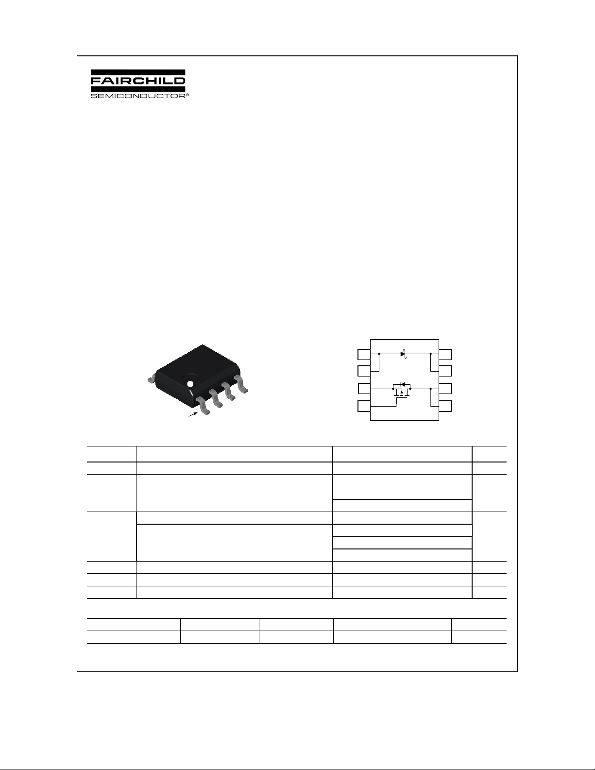
FDFS2P103A
Integrated P-Channel PowerTrench
MOSFET and Schottky Diode
FDFS2P103
General Description
The FDFS2P103A combines the exceptional
performance of Fairchild's PowerTrench MOSFET
technology with a very low forward voltage drop
Schottky barrier recti fier in an SO-8 package.
This device is designed specifically as a single package
solution for DC to DC converters. It features a fast
switching, low gate charge MOSFET with very low onstate resistance. The independently connected
Schottky diode allows its use in a variety of DC/DC
converter topologies.
D
D
C
C
SO-8
Pin 1
A
Absolute Maximum Ratings T
G
S
A
o
=25
C unless otherwise noted
A
Features
• –5.3 A, –30V R
R
• V
< 0.35 V @ 1 A (TJ = 125°C)
F
V
< 0.25 V @ 1 A (TJ = 25°C)
F
• Schottky and MOSFET incorporated into single
power surface mount SO-8 package
• Electrically independent S chottky and MOSFET
pinout for design flexibility
A
A
S
G
= 59 mΩ @ VGS = –10 V
DS(ON)
= 92 mΩ @ VGS = –4.5 V
DS(ON)
81
72
63
54
C
C
D
D
Symbol Parameter Ratings Units
V
MOSFET Drain-Source Voltage
DSS
V
MOSFET Gate-Source Voltage
GSS
ID Drain Current – Continuous (Note 1a)
– Pulsed
PD
TJ, T
STG
V
Schottky Repetiti ve P eak Reverse Voltage 30 V
RRM
IO Schottky Average Forward Current (Note 1a) 1 A
Power Dissipation for Dual Operation 2
Power Dissipation for Single Operation (Note 1a) 1.6
(Note 1b)
Operating and Storage Junction Temperature Range
(Note 1c)
–30
±25
–5.3
–20
1
0.9
–55 to +150
V
V
A
W
°C
Package Marking and Ordering Information
Device Marking Device Reel Size Tape width Quantity
FDFS2P103A FDFS2P103A 13’’ 12mm 2500 units
2002 Fairchild Semiconductor Corporation
FDFS2P103A Rev C (W)
Page 2
FDFS2P103A
Electrical Characteristics T
= 25°C unless otherwise noted
A
Symbol Parameter Test Conditions Min Typ Max Units
Off Characteristics
BV
Drain–Source Breakdown Voltage
DSS
∆BVDSS
∆T
I
Zero Gate Voltage Drain Current VDS = –24 V, VGS = 0 V –1
DSS
I
Gate–Body Leakage VGS = ±25 V, VDS = 0 V ±100 nA
GSS
Breakdown Voltage Temperature
Coefficient
J
= 0 V, ID = –250 µA
V
GS
I
= –250 µA,
D
Referenced to 25°C
–30 V
–22
mV/°C
µA
On Characteristics (Note 2)
V
Gate Threshold Voltage
GS(th)
∆VGS(th)
∆TJ
R
DS(on)
Gate Threshold Voltage
Temperature Coefficient
Static Drain–Source
On–Resistance
= VGS, ID = –250 µA
V
DS
I
= –250 µA,
D
Referenced to 25°C
VGS = –10 V, ID = –5.3 A
= –4.5 V, ID = –4 A
V
GS
=–10 V, ID = –5.3A, TJ=125°C
V
GS
gFS Forward Transconductance VDS = –5V, ID = –5.3 A 8.9 S
–1 –1.8 –3 V
4.2
50
76
68
59
92
88
mV/°C
mΩ
Dynamic Characteristics
C
Input Capacitance 535 pF
iss
C
Output Capacitance 135 pF
oss
C
Reverse Transfer Capacitance
rss
RG Gate Resistance V
= –15 V, VGS = 0 V,
V
DS
f = 1.0 MHz
= 0 V, f = 1.0 MHz 4.7
GS
75 pF
Ω
Switching Characteristics (Note 2)
t
Turn–On Delay Time
d(on)
tr Turn–On Rise Time 16 28 ns
t
Turn–Off Delay Time 15 26 ns
d(off)
= –15 V, ID = –1 A,
V
DD
= –10 V, R
V
GS
GEN
= 6 Ω
tf Turn–Off Fall Time
Qg Tot al Gat e Charge 5.7 8 nC
= –15 V, ID = –5.3 A,
V
Qgs Gate–Source Charge 1.8 nC
Qgd Gate–Drain Charge
DS
V
GS
= –5 V
11 21 ns
10 19 ns
2.4 nC
Drain–Source Diode Characteristics and Maximum Ratings
IS Maximum Continuous Drain–Source Diode Forward Current –1.3 A
VSD
Drain–Source Diode Forward
Voltage
V
= 0 V, IS = –1.3 A (Note 2)
GS
–0.8 –1.2
Schottky Diode Characteristics
IR Reverse Leakage VR = 30 V 160 500
225 280 mV
80 250 mV
305 350 mV
185 250 mV
380 420 mV
FDFS2P103A Rev C (W)
VF Forward Voltage
IF = 0.1A
IF = 1A
I
= 3A
F
TJ = 25°C
T
= 125°C
J
TJ = 25°C
= 125°C
T
J
= 25°C
T
J
µA
V
Page 3

Thermal Characteristics
R
θJA
R
θJA
R
θJC
Notes:
1. R
is the sum of the junction-to-case and case-to-ambient thermal resistance where the case thermal reference is defined as the solder mounting surface of
θJA
the drain pins. R
Thermal Resistance, Junction-to-Ambient
Thermal Resistance, Junction-to-Ambient
Thermal Resistance, Junction-to-Case
is guaranteed by design while R
θJC
is determined by the user's board design.
θCA
(Note 1a) 78
(Note 1c) 135
(Note 1) 40
FDFS2P103A
°C/W
°C/W
°C/W
a) 78°C/W when
mounted on a
0.5in2 pad of 2
oz copper
Scale 1 : 1 on letter size paper
2. Pulse Test: Pulse Width < 300µs, Duty Cycle < 2.0%
b) 125°C/W when
mounted on a
0.02 in2 pad of
2 oz copper
c) 135°C/W when
mounted on a
minimum pad.
FDFS2P103A Rev C (W)
Page 4

)
E
E
)
)
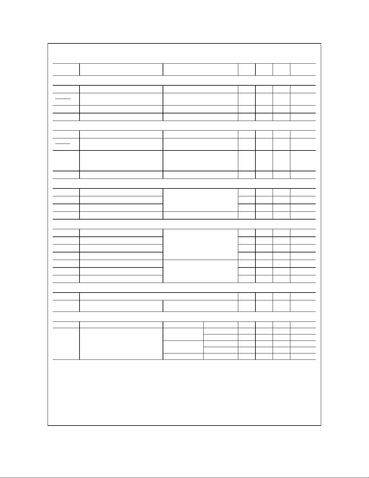
Typical Characteristics
FDFS2P103A
20
VGS = -10V
16
-6.0V
12
8
4
, DRAIN-SOURCE CURRENT (A
D
-I
0
012345
-5.0V
-4.5V
-V
, DRAIN-SOURCE VOL TAGE ( V )
DS
-4.0V
-3.5V
-3.0V
5.00
VGS = -3.0V
4.00
3.00
, NORMALIZED
2.00
DS(ON)
R
1.00
DRAIN-SOURCE ON-RESISTANC
0.00
0 4 8 12 16
-3.5V
-4.0V
-4.5V
- I
, DRAIN CURRENT (A)
D
-5.0V
-6.0V
Figure 1. On-Region Characteristics. Figure 2. On-Resistance Variation with
Drain Current and Gate Voltage.
1.6
1.4
1.2
, NORMALIZED
DS(ON)
R
0.8
DRAIN-SOURCE ON-RESISTANC
0.6
ID = -5.3A
V
= -10V
GS
1
-50 0 50 100 150
T
, JUNCTION TEMPERATURE (oC)
J
0.22
0.16
TA = 125oC
0.1
, ON-RESISTANCE (OHM)
DS(ON)
R
0.04
TA = 25oC
0246810
-V
, GATE TO SOURCE V O LTAGE (V)
GS
-10V
ID = -2.65A
Figure 3. On-Resistance Variation with
Temperature.
10
VDS = -5V
8
6
4
, DRAIN CURRENT (A
D
-I
2
0
12345
125oC
, GATE TO SOURCE VOLTAGE (V)
-V
GS
25oC
TA = -55oC
Figure 4. On-Resistance Variation with
Gate-to-Source Voltage.
100
VGS = 0V
10
1
0.1
0.01
0.001
, REVERSE DRAIN CURRENT (A
S
-I
0.0001
0 0.2 0.4 0.6 0.8 1 1.2 1.4
TA = 125oC
25oC
-55oC
, BODY DIODE FORWARD VOLTAGE (V)
-V
SD
Figure 5. Transfer Characteristics. Figure 6. Body Diode Forward Voltage Variation
with Source Current and Temperature.
FDFS2P103A Rev C (W)
Page 5

)
Typical Characteristics
FDFS2P103A
10
ID = -5.3A VDS = -10V
8
6
4
2
, GATE-SOURCE VOLTAGE (V)
GS
-V
0
024681012
, GATE CHARGE (nC)
Q
g
-15V
-20V
800
600
C
iss
400
C
CAPACITANCE (pF)
200
C
0
rss
0 5 10 15 20
oss
-V
, DRAIN TO SOURCE VOLTAGE (V)
DS
Figure 7. Gate Charge Characteristics. Figure 8. Capacitance Characteristics.
10
1
0.1
0.01
, FORWARD LEAKAGE CURRENT (A)
F
I
0.001
0 0.1 0.2 0.3 0.4
TJ = 125oC
TJ = 25oC
VF, FORWARD VOLTAGE (V)
1
0.1
0.01
0.001
0.0001
0.00001
, REVERSE LEAKAGE CURRENT (A
R
I
0.000001
0 5 10 15 20 25 30
TJ = 125oC
TJ = 25oC
VR, REVERSE VOLTAGE (V)
f = 1MHz
V
= 0 V
GS
Figure 9. Schottky Diode Forward Voltage. Figure 10. Schottky Diode Reverse Current.
1
D = 0.5
0.2
0.1
r(t), NORMALIZED EFFECTIVE
TRANSIENT THERMAL RESISTANCE
0.01
0.1
0.05
0.02
0.01
SINGLE PULSE
R
(t) = r(t) + R
JA
θ
R
= 135 °C/W
θJA
P(pk)
t
1
t
2
T
- TA = P * R
J
Duty Cycle, D = t
JA
θ
(t)
θJA
/ t
1
2
0.001 0.01 0.1 1 10 100 1000
Figure 11. Transient Thermal Response Curve.
Thermal characterization performed using the conditions described in Note 1c.
Transient thermal response will change depending on the circuit board design.
FDFS2P103A Rev C (W)
Page 6

TRADEMARKS
The following are registered and unregistered trademarks Fairchild Semiconductor owns or is authorized to use and is
not intended to be an exhaustive list of all such trademarks.
ACEx
ActiveArray
Bottomless
CoolFET
CROSSVOL T
DOME
EcoSPARK
E2CMOS
EnSigna
TM
TM
FACT
FACT Quiet Series
â
FAST
FASTr
FRFET
GlobalOptoisolator
GTO
HiSeC
I2C
Across the board. Around the world.
The Power Franchise
Programmable Active Droop
ImpliedDisconnect
ISOPLANAR
LittleFET
MicroFET
MicroPak
MICROWIRE
MSX
MSXPro
OCX
OCXPro
OPTOLOGIC
â
OPTOPLANAR
PACMAN
POP
Power247
PowerTrench
â
QFET
QS
QT Optoelectronics
Quiet Series
RapidConfigure
RapidConnect
SILENT SWITCHER
SMART START
SPM
Stealth
SuperSOT-3
SuperSOT-6
SuperSOT-8
SyncFET
TinyLogic
TruTranslation
UHC
UltraFET
â
VCX
â
DISCLAIMER
FAIRCHILD SEMICONDUCTOR RESERVES THE RIGHT TO MAKE CHANGES WITHOUT FURTHER
NOTICE TO ANY PRODUCTS HEREIN TO IMPROVE RELIABILITY, FUNCTION OR DESIGN. FAIRCHILD
DOES NOT ASSUME ANY LIABILITY ARISING OUT OF THE APPLICATION OR USE OF ANY PRODUCT
OR CIRCUIT DESCRIBED HEREIN; NEITHER DOES IT CONVEY ANY LICENSE UNDER ITS PATENT
RIGHTS, NOR THE RIGHTS OF OTHERS.
LIFE SUPPORT POLICY
FAIRCHILDS PRODUCTS ARE NOT AUTHORIZED FOR USE AS CRITICAL COMPONENTS IN LIFE SUPPORT
DEVICES OR SYSTEMS WITHOUT THE EXPRESS WRITTEN APPROVAL OF FAIRCHILD SEMICONDUCTOR CORPORATION.
As used herein:
1. Life support devices or systems are devices or
systems which, (a) are intended for surgical implant into
the body, or (b) support or sustain life, or (c) whose
failure to perform when properly used in accordance
with instructions for use provided in the labeling, can be
reasonably expected to result in significant injury to the
user.
PRODUCT STATUS DEFINITIONS
Definition of Terms
Datasheet Identification Product Status Definition
Advance Information
Preliminary
No Identification Needed
Formative or
In Design
First Production
Full Production
2. A critical component is any component of a life
support device or system whose failure to perform can
be reasonably expected to cause the failure of the life
support device or system, or to affect its safety or
effectiveness.
This datasheet contains the design specifications for
product development. Specifications may change in
any manner without notice.
This datasheet contains preliminary data, and
supplementary data will be published at a later date.
Fairchild Semiconductor reserves the right to make
changes at any time without notice in order to improve
design.
This datasheet contains final specifications. Fairchild
Semiconductor reserves the right to make changes at
any time without notice in order to improve design.
Obsolete
Not In Production
This datasheet contains specifications on a product
that has been discontinued by Fairchild semiconductor.
The datasheet is printed for reference information only.
Rev. I1
 Loading...