

Page 1

FDC87W21
Power I/O Controller with Fast Infrared Support
FEATURES
• 5 Volt Operation
• Plug & Play 1.0A Compliant
• Supports Eight IRQs, Four DMA Channels,
480 Relocatable Addresses
• Floppy Disk Controller (FDC)
- Compatible with IBM PC/AT Disk Drive
Systems
- Variable Write Precompensation with
Track Selectable Capability
- DMA Enable Logic
- Supports Floppy Disk Drives and Tape
Drives
- Detects All Over-Run and Under-Run
Conditions
- Data Rate and Drive Control Registers
- Built-in Address Mark Detection Circuit
to Simplify the Read Electronics
- IBM PC System Address Decoder
- 24 MHz Crystal Input (48 MHz when for
2 Mbps Fast Tape Drive)
- FDD Anti-Virus Functions with Software
Write Protect and FDD Write Enable
Signal (Write Data Signal Was Forced
to Be Inactive)
- Supports up to Four 3.5-Inch or 5.25Inch Floppy Disk Drives
- Completely Compatible with Industry
Standard 82077/ 765A
- Supports
360K/720K/1.2M/1.44M/2.88M Format;
250 Kbps, 300 Kbps, 500 Kbps, 1
Mbps, 2 Mbps Data Transfer Rate
- Supports Perpendicular Recording
Format
- Supports 3-Mode FDD and Win95
Driver
- 16-Byte Data FIFOs
• Serial Ports
- Two High-Speed 16550 Compatible
UARTs with 16-Byte Send/Receive
FIFOs
- MIDI Compatible
- Fully Programmable Serial-Interface
Characteristics:
- 5, 6, 7 or 8-Bit Characters
- Even, Odd or No Parity Bit
Generation/Detection
- 1, 1.5 or 2 Stop Bits Generation
- Internal Diagnostic Capabilities:
- Loop-Back Controls For
Communications Link Fault
Isolation
- Break, Parity, Overrun, Framing
Error Simulation
- Programmable Baud Generator Allows
Division of 1.8461 MHz and 24 MHz by
1 to (216-1)
- Maximum Baud Rate Is up to 911.6 (8
times of 115.2 Kbps) for 1.8461 MHz
and 1.5 Mbps for 24 MHz
• Infrared
- Supports IrDA Version 1.0 SIR Protocol
with Maximum Baud Rate up to 115.2
Kbps
- Supports SHARP ASK-IR Protocol with
Maximum Baud Rate up to 57600 bps
- Supports IrDA Version 1.1 MIR (1.152
Mbps) and FIR (4 Mbps) Protocol
- Two DMA Channel for Transmitter
and Receiver
- 32-Byte FIFO is Supported in the
TX/RX Terminal
Page 2

2
- 8-Byte Status FIFO Is Supported
to Store Received Frame Status
(Such as Overrun, CRC Error,
Etc.)
- Supports Auto-Config SIR and FIR
• Parallel Port
- Compatible with IBM Parallel Port
- Supports Parallel Port with Bi-
Directional Lines
- Supports Enhanced Parallel Port (EPP)
− Compatible with IEEE 1284
Specification
- Supports Extended Capabilities Port
(ECP) − Compatible with IEEE 1284
Specification
- Extension FDD Mode Supports Disk
Drive B; and Extension 2FDD Mode
Supports Disk Drives A and B Through
Parallel Port
- Extension Adapter Mode Supports
Pocket Devices Through Parallel Port
- JOYSTICK Mode Supports Joystick
Through Parallel Port
• ISA Host Interface
• IDE
- Supports up to Two Embedded Hard
Disk Drives (IDE AT BUS)
• Programmable Configuration Settings
• Immediate or Automatic Power-Down Mode
for Power Management
• All Hardware Power-On Settings Have
Internal Pull-Up or Pull-Down Resistors as
Default Value
• 100 Pin QFP Package
GENERAL DESCRIPTION
The FDC87W21 is an enhanced version of the
FDC87W22 --- which integrates the disk drive
adapter, serial port (UART), IrDA 1.0 SIR,
parallel port, IDE interface, configurable plugand-play registers for the whole chip --- adding
powerful features: IrDA 1.1 (MIR for 1.152 Mbps
or FIR for 4 Mbps), TV remote IR. In addition to
the function enhancement, FDC87W21 is pin-topin compatible to FDC87W22.
The disk drive adapter functions of the
FDC87W21 include a floppy disk drive controller
compatible with the industry standard
82077/765 data separator, write precompensation circuit, decode logic, data rate
selection, clock generator, drive interface control
logic, interrupt and DMA logic. The wide range
of functions integrated into the FDC87W21
greatly reduces the number of components
required for interfacing with floppy disk drives.
The FDC87W21 supports up to 4 Three-mode
Floppy Disk Drives (FDD) of formats 360K,
720K, 1.2M, 1.44M, or 2.88M, and data transfer
rates of 250 Kbps, 300 Kbps, 500 Kbps, 1
Mbps, and 2 Mbps.
The FDC87W21 provides two high-speed serial
communication ports (UARTs), one of which
supports serial Infrared communication. Each
UART includes a 16-byte send/receive FIFO, a
programmable baud rate generator, complete
modem control capability, and a processor
interrupt system. One of UART supports infrared
(IR) includes 32-byte FIFO, serial IR (115, 200
bps), MIR (1.152 Mbps or 0.576 Mbps), FIR (4
Mbps), and TV remote IR (supported NEC, RC5, extended RC-5, and RECS-80 protocols).
The FDC87W21 supports one PC-compatible
printer port (SPP), bi-directional Printer Port
(BPP), and also Enhanced Parallel Port (EPP)
and Extended Capabilities Port (ECP).
Through the printer port interface pins, also
available are: Extension FDD Mode and
Extension 2FDD Mode allowing one or two
external floppy disk drives to be attached.
Especially in the application of notebook
computer, this feature is very useful.
The Extension Adapter Mode of the FDC87W21
also allows pocket devices to be installed
through the printer interface pins in notebook
computer applications according to a protocol
set by SMSC, but with upgraded performance.
The JOYSTICK mode allows a joystick to be
connected to a parallel port with a signal
switching cable.
Page 3

3
The FDC87W21 supports two embedded hard
disk drive (IDE AT bus) interfaces and a game
port with decoded read/write output.
The configuration registers support mode
selection, function enable/disable, and power
down function selection. Moreover, the
configurable PnP registers are compatible with
the plug-and-play feature in Windows 95,
which makes system resource allocation more
efficient than ever.
Standard Microsystems is a registered trademark and
SMSC is a trademark of Standard Microsystems
Corporation. Other product and company names are
trademarks or registered trademarks of their respective
holders.
Page 4

4
TABLE OF CONTENTS
FEATURES....................................................................................................................................... 1
GENERAL DESCRIPTION ................................................................................................................ 2
PIN CONFIGURATION...................................................................................................................... 6
PIN DESCRIPTION ........................................................................................................................ 7
HOST INTERFACE..............................................................................................................................7
FDC FUNCTIONAL DESCRIPTION................................................................................................. 17
FDC87W21 FDC..........................................................................................................................17
REGISTER DESCRIPTIONS........................................................................................................ 31
IDE.................................................................................................................................................. 42
IDE DECODE DESCRIPTION .............................................................................................................. 42
UART PORT ................................................................................................................................... 43
UNIVERSAL ASYNCHRONOUS RECEIVER/TRANSMITTER (UART A, UART B)............................................ 43
REGISTER ADDRESS........................................................................................................................ 43
IR PORT........................................................................................................................................ 54
PARALLEL PORT........................................................................................................................... 83
PRINTER INTERFACE LOGIC ..................................................................................................... 83
ENHANCED PARALLEL PORT (EPP)..........................................................................................85
EXTENDED CAPABILITIES PARALLEL (ECP) PORT.................................................................. 89
EXTENSION FDD MODE (EXTFDD).................................................................................................. 98
EXTENSION 2FDD MODE (EXT2FDD) .............................................................................................. 98
EXTENSION ADAPTER MODE (EXTADP) (PATENT PENDING) ................................................................. 98
JOYSTICK MODE (PATENT PENDING)................................................................................................... 99
GAME PORT DECODER ...............................................................................................................100
PLUG AND PLAY CONFIGURATION ............................................................................................100
EXTENDED FUNCTION REGISTERS ............................................................................................100
EXTENDED FUNCTIONS ENABLE REGISTERS (EFERS)..........................................................................101
EXTENDED FUNCTION INDEX REGISTERS (EFIRS), EXTENDED FUNCTION DATA REGISTERS (EFDRS) ........101
BIT MAP CONFIGURATION REGISTERS ...............................................................................................137
SPECIFICATIONS..........................................................................................................................139
ABSOLUTE MAXIMUM RATINGS..........................................................................................................139
DC CHARACTERISTICS .............................................................................................................139
AC CHARACTERISTICS....................................................................................................................141
TIMING WAVEFORMS ..................................................................................................................147
FDC............................................................................................................................................147
UART/PARALLEL...........................................................................................................................149
MODEM CONTROL TIMING................................................................................................................150
PARALLEL PORT.............................................................................................................................151
PARALLEL PORT TIMING ..................................................................................................................151
EPP DATA OR ADDRESS READ CYCLE (EPP VERSION 1.9)..................................................................152
EPP DATA OR ADDRESS WRITE CYCLE (EPP VERSION 1.9)................................................................153
EPP DATA OR ADDRESS READ CYCLE (EPP VERSION 1.7)..................................................................154
Page 5

5
EPP DATA OR ADDRESS WRITE CYCLE (EPP VERSION 1.7)................................................................155
PARALLEL PORT FIFO TIMING .........................................................................................................155
ECP PARALLEL PORT FORWARD TIMING ...........................................................................................156
ECP PARALLEL PORT REVERSE TIMING.............................................................................................156
EXTENSION ADAPTER MODE COMMAND CYCLE ...................................................................................157
EXTENSION ADAPTER MODE INTERRUPT CYCLE..................................................................................157
EXTENSION ADAPTER MODE DMA CYCLE..........................................................................................158
APPLICATION CIRCUITS..............................................................................................................158
PARALLEL PORT EXTENSION FDD ....................................................................................................158
PARALLEL PORT EXTENSION FDD ....................................................................................................159
PARALLEL PORT EXTENSION 2FDD ..................................................................................................160
PARALLEL PORT JOYSTICK MODE .....................................................................................................161
FOUR FDD MODE..........................................................................................................................161
PACKAGE DIMENSIONS ..............................................................................................................162
80 Arkay Drive
Hauppauge, NY 11788
(516) 435-6000
FAX (516) 273-3123
Page 6
6
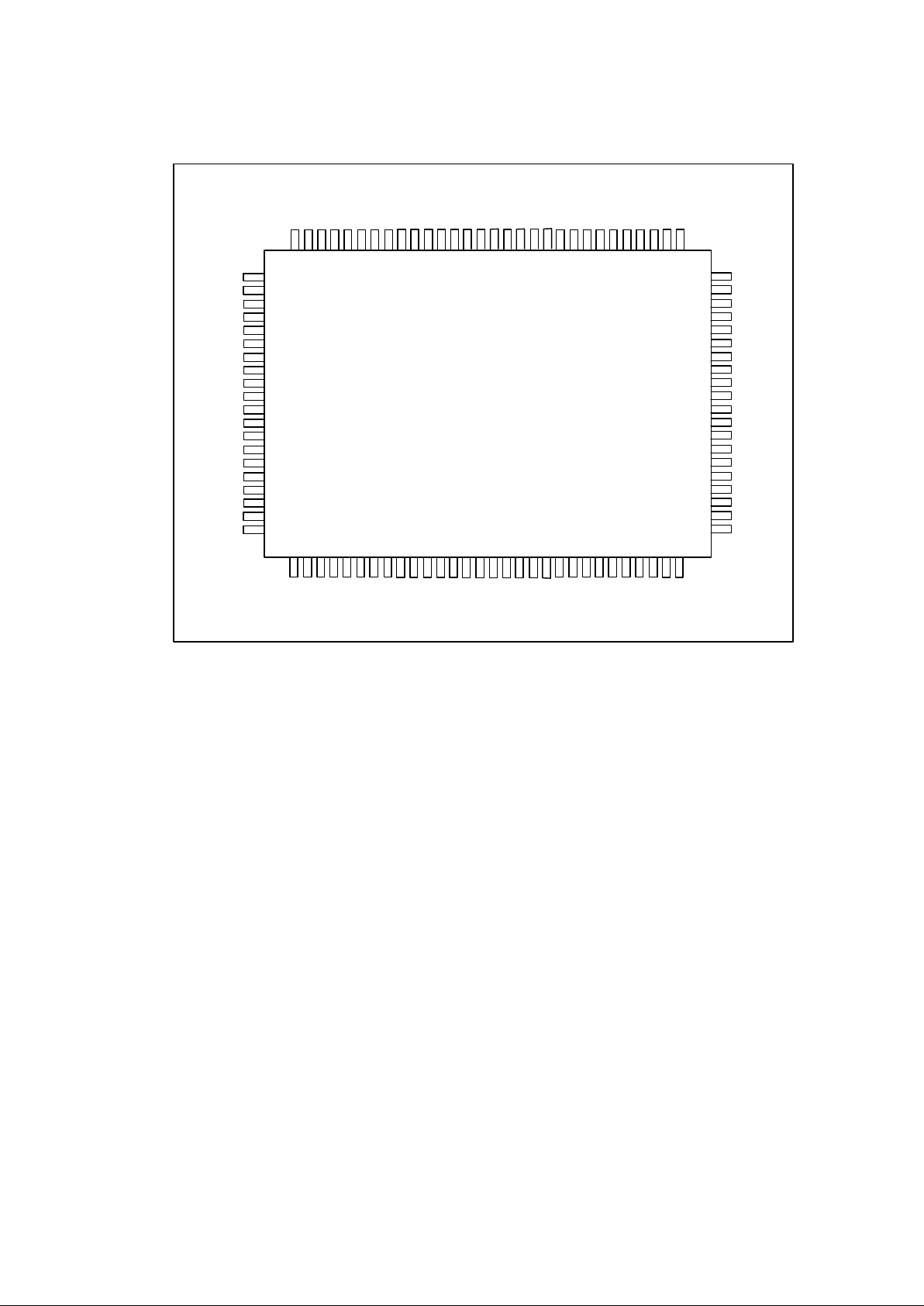
PIN CONFIGURATION
81
82
83
84
85
86
87
88
89
90
91
92
93
94
95
96
97
98
99
100
nINDEX
nSTEP
nDSA
nDSB
nWE
nWD
nRWC
nHEAD
nDIR
GND
nIDBEN
IRQ_B
nIRQIN
nCS0
nCS1
IRQ_A
TC
nDACK_B
IRQ_F
DRQ_B
nMOB
nMOA
nTRAK0
NWP
nDSKCHG
A10
nRDATAD7D6D5D4D3D2D1D0
GND
nIOW
nIOR
AENA9A8A7A6A5VDDA4A3A2A1
A0
8079787776757473727170696867666564636261605958575655545352
51
nRIB
nDCDB
nDSRB
nCTSB
nDTRB
nRTSB
IRQ_C
SOUTB
SINB
nGMRD
GND
nGMWR
SOUTA
IRQ_D
nRTSA
nDTRA
nCTSA
nDSRA
nDCDA
nRIA
50
49
48
47
46
45
44
43
42
41
40
39
38
37
36
35
34
33
32
31
1234567891011121314151617181920212223242526272829
30
nRESIDE
nCS
nPDCIN
DRQ_C
IOCHRDY
MR
XTAL1
XTAL2
PD0
PD1
PD2
PD3
PD4
PD5
VDD
PD6
PD7
nDACK_C
nSTB
nAFD
nINIT
nSLIN
IRQ_E
BUSY
GND
nACK
PE
SLCT
nERR
SINA
FDC87W21
Page 7

PIN DESCRIPTION
(Note: Refer to the DC Characteristics Section for details.)
I/O8tc TTL level output pin with 8 mA source-sink capability; CMOS level input voltage
I/O12t TTL level bi-directional pin with 12 mA source-sink capability
I/O24t TTL level bi-directional pin with 24 mA source-sink capability
OUT8t TTL level output pin with 8 mA source-sink capability
OUT12t TTL level output pin with 12 mA source-sink capability
OD12 Open-drain output pin with 12 mA sink capability
OD24 Open-drain output pin with 24 mA sink capability
INt TTL level input pin
INts TTL level Schmitt-triggered input pin
INc CMOS level input pin
INcs CMOS level Schmitt-triggered input pin
Host Interface
SYMBOL PIN I/O FUNCTION
HOST INTERFACE
D0−D7
66-73 I/O
24t
System data bus bits 0-7
A0−A9
51-55
57-61
IN
t
System address bus bits 0-9
A10 75 IN
t
In ECP Mode, this pin is the A10 address input.
IOCHRDY 5 OD
24
In EPP Mode, this pin is the IO Channel Ready output to extend the
host read/write cycle.
MR 6 IN
ts
Master Reset. Active high. MR is low during normal operations.
nCS
nDACK_N
IRSL1
IRSL2
2 IN
t
IN
t
OUT
12t
OUT
12t
Active low chip select signal.
DMA acknowledge signal D.
IR module mode select 1.
IR module mode select 2.
AEN 62 IN
t
System address bus enable
nIOR 63 IN
ts
CPU I/O read signal
nIOW 64 IN
ts
CPU I/O write signal
DRQ_B 100 OUT
12t
DMA request signal B
nDACK_B 98 IN
ts
DMA Acknowledge signal B
DRQ_C 4 OUT
12t
DMA request signal C
nDACK_C 18 IN
ts
DMA Acknowledge signal C
TC 97 IN
ts
Terminal Count. When active, this pin indicates termination of a
DMA transfer.
IRQIN
DRQ_D
IRSL2
IRRXH/
IRSL0
93 IN
t
OUT
12t
OUT
12t
I/O
12t
Interrupt request input.
DMA request signal D.
IR module mode selection 2.
When input, act as a function of high speed IR receiving terminal.
When output selected, act as a IR module mode selection 0.
IRQ_A
GIO1
96 OUT
12t
I/O
12t
When CR16 Bit 4 (GOIQSEL) = 0: Interrupt request signal A;
When CR16 Bit 4 (GOIQSEL) = 1: General Purpose I/O port 1.
IRQ_B
GIO0
92 OUT
12t
I/O
12t
When CR16 Bit 4 (GOIQSEL) = 0: Interrupt request signal B;
When CR16 Bit 4 (GOIQSEL) = 1: General Purpose I/O port 0.
IRQ_C 44 OUT
12t
Interrupt request signal C
Page 8

8
SYMBOL PIN I/O FUNCTION
IRQ_D 37 OUT
12t
Interrupt request signal D
IRQ_E 23 OUT
12t
Interrupt request signal E
IRQ_F 99 OUT
12t
Interrupt request signal F
XTAL1 7 CLK IN XTAL oscillator input
XTAL2 8 CLK
OUT
XTAL oscillator output
SERIAL PORT INTERFACE
nCTSA
nCTSB
34
47
IN
t
IN
t
Clear To Send is the modem control input.
The function of these pins can be tested by reading Bit 4 of the
handshake status register.
nDSRA
nDSRB
33
48
IN
t
IN
t
Data Set Ready. An active low indicates the modem or data set is
ready to establish a communication link and transfer data to the
UART.
nDCDA
nDCDB
32
49
IN
t
IN
t
Data Carrier Detect. An active low indicates the modem or data set
has detected a data carrier.
nRIA
nRIB
31
50
IN
t
IN
t
Ring Indicator. An active low indicates that a ring signal is being
received by the modem or data set.
SINA
SINB/
IRRX1
30
42
IN
t
IN
t
Serial Input. Used to receive serial data from the communication
link.
SOUTA
PIN2IPSEL
38 O
8tc
I
8tc
UART A Serial Output. Used to transmit serial data out to the
communication link.
During power-on reset, this pin is pulled up internally and is defined
as PIN2IPSEL, which provides the power-on value for CR16 bit 1
(PIN2IPSEL). A 4.7 k is recommended when intends to pull down
at power-on reset.
SOUTB
IRTX1
PGMDRQ
43 O
8tc
O
8tc
I
8tc
UART B Serial Output. Used to transmit serial data out to the
communication link.
During power-on reset, this pin is pulled down internally and is
defined as PGMDRQ, which provides the power-on value for CR16
bit 3 (GMDRQ). A 4.7 k is recommended when intends to pull up
at power-on reset.
nDTRA
PHEFRAS
35 O
8tc
I
8tc
UART A Data Terminal Ready. An active low informs the modem
or data set that the controller is ready to communicate.
During power-on reset, this pin is pulled down internally and is
defined as PHEFRAS, which provides the power-on value for CR16
bit 0 (HEFRAS). A 4.7 k is recommended when intends to pull up
at power-on reset.
nDTRB 46 O
8t
UART B Data Terminal Ready. An active low informs the modem
or data set that controller is ready to communicate.
nRTSA
PPNPCVS
36 O
8tc
I
8tc
UART A Request To Send. An active low informs the modem or
data set that the controller is ready to send data.
During power-on reset, this pin is pulled up internally and is defined
as PPNPCVS, which provides the power-on value for CR16 bit 2
(PNPCVS). A 4.7 k is recommended when intends to pull down
at power-on reset.
Page 9

9
SYMBOL PIN I/O FUNCTION
nRTSB
PGOIQSEL
45 O
8tc
I
8tc
UART B Request To Send. An active low informs the modem or
data set that the controller is ready to send data.
During power-on reset, this pin is pulled down internally and is
defined as PGOIQSEL, which provides the power-on value for
CR16 bit 4 (GOIQSEL). A 4.7 k is recommended when intends to
pull up at power-on reset.
Game Port/Power Down Interface
If Bit 3 of CR16 (GMDRQ) is 1, Bit 4 of CR3 (GMODS0) determines whether the game port is in
Adapter mode or Portable mode (default is Adapter mode). If Bit 3 of CR16 is 0, pin 39 and 41 are
used for DMA A operation.
nGMRD 41 OUT8tWhen CR16 Bit 3 (GMDRQ) = 1, Adapter mode: Game port read
control signal.
PFDCEN OUT8tPortable mode: When parallel port is selected as Extension
FDD/Extension 2FDD mode, this pin will be active. The active state
is dependent on bit 7 of CRA (PFDCACT), and default is low active.
nDACK_A IN
t
When CR16 Bit 3 (GMDRQ) = 0, DMA acknowledge signal A.
nGMWR 39 OUT8tWhen CR16 Bit 3 (GMDRQ) = 1, Adapter mode: Game port write
control signal.
PEXTEN OUT8tPortable mode: When a particular extended mode is selected for
the parallel port, this pin will be active. The extended modes
include Extension Adapter mode, EPP mode, ECP mode, and
ECP/EPP mode, which are selected using bit 3 - bit 0 of CRA. The
active state is dependent on bit 6 of CRA (PEXTACT); the default is
low active.
DRQ_A OUT8tWhen CR16 Bit 3 (GMDRQ) = 0: DMA request signal A.
PDCIN 3 IN
t
This input pin controls the chip power down. When this pin is
active, the clock supply to the chip will be inhibited and the output
pins will be tri-stated as defined in CR4 and CR6. The PDCIN is
pulled down internally. Its active state is defined by bit 4 of CRA
(PDCHACT). Default is high active.
nDACK_N IN
t
DMA acknowledge signal D.
IRSL1 OUT
12t
IR module mode select 1.
IRRXH/
IRSL0
I/O
12t
When input pin, high speed IR received terminal. When as output
pin, IR module mode select 0. Input or output are definied in high
speed IR register.
Multi-Mode Parallel Port
The following pins have eight functions, which are controlled by bits PRTMOD0, PRTMOD1, and
PRTMOD2 of CR0 and CR9. (Refer to the Extended Functions Section).
Page 10

10
SYMBOL PIN I/O FUNCTION
BUSY 24 IN
t
OD
12
IN
t
OD
12
-
PRINTER MODE: BUSY
An active high input indicates that the printer is not ready to receive
data. This pin is pulled high internally. Refer to the description of
the parallel port for the definition of this pin in ECP and EPP mode.
EXTENSION FDD MODE: nMOB2
This pin is for Extension FDD B; the function of this pin is the same
as that of the nMOB pin.
EXTENSION ADAPTER MODE: XIRQ
This pin is an interrupt request generated by the Extension Adapter
and is an active high input.
EXTENSION 2FDD MODE: nMOB2
This pin is for Extension FDD A and B; the function of this pin is the
same as that of the nMOB pin.
JOYSTICK MODE: NC pin.
nACK 26 IN
t
OD
12
IN
t
OD
12
-
PRINTER MODE: nACK
An active low input on this pin indicates that the printer has
received data and is ready to accept more data. This pin is pulled
high internally. Refer to the description of the parallel port for the
definition of this pin in ECP and EPP mode.
EXTENSION FDD MODE: nDSB2
This pin is for the Extension FDD B; its functions are the same as
those of the nDSB pin.
EXTENSION ADAPTER MODE: XDRQ
DMA request generated by the Extension Adapter. An active high
input.
EXTENSION 2FDD MODE: nDSB2
This pin is for Extension FDD A and B; this function of this pin is
the same as that of the nDSB pin.
JOYSTICK MODE: NC pin.
PE 27 IN
t
OD
12
OUT
12t
OD
12
-
PRINTER MODE: PE
An active high input on this pin indicates that the printer has
detected the end of the paper. This pin is pulled high internally.
Refer to the description of the parallel port for the definition of this
pin in ECP and EPP mode.
EXTENSION FDD MODE: nWD2
This pin is for Extension FDD B; its function is the same as that of
the nWD pin.
EXTENSION ADAPTER MODE: XA0
This pin is system address A0 for the Extension Adapter
EXTENSION 2FDD MODE: nWD2
This pin is for Extension FDD A and B; this function of this pin is
the same as that of the nWD pin.
JOYSTICK MODE: NC pin.
Page 11

11
SYMBOL PIN I/O FUNCTION
SLCT 28 IN
t
OD
12
OUT
12t
OD
12
-
PRINTER MODE: SLCT
An active high input on this pin indicates that the printer is selected.
This pin is pulled high internally. Refer to the description of the
parallel port for the definition of this pin in ECP and EPP mode.
EXTENSION FDD MODE: WE2
This pin is for Extension FDD B; its functions are the same as
those of the nWE pin.
EXTENSION ADAPTER MODE: XA1
This pin is system address A1 for the Extension Adapter.
EXTENSION 2FDD MODE: nWE2
This pin is for Extension FDD A and B; this function of this pin is
the same as that of the nWE pin.
JOYSTICK MODE: NC pin.
nERR 29 IN
t
OD
12
OUT
12t
OD
12
-
PRINTER MODE: nERR
An active low input on this pin indicates that the printer has
encountered an error condition. This pin is pulled high internally.
Refer to the description of the parallel port for the definition of this
pin in ECP and EPP mode.
EXTENSION FDD MODE: nHEAD2
This pin is for Extension FDD B; its function is the same as that of
the nHEAD pin.
EXTENSION ADAPTER MODE: XA2
This pin is system address A2 for the Extension Adapter.
EXTENSION 2FDD MODE: nHEAD2
This pin is for Extension FDD A and B; its function is the same as
that of the nHEAD pin.
JOYSTICK MODE: NC pin.
nSLIN 22 OD
12
OD
12
OUT
12t
OD
12
OUT
12t
PRINTER MODE: nSLIN
Output line for detection of printer selection. This pin is pulled high
internally. Refer to the description of the parallel port for the
definition of this pin in ECP and EPP mode.
EXTENSION FDD MODE: nSTEP2
This pin is for Extension FDD B; its function is the same as that of
the nSTEP pin.
EXTENSION ADAPTER MODE: XTC
This pin is the DMA terminal count for the Extension Adapter. The
count is sent by TC directly.
EXTENSION 2FDD MODE: nSTEP2
This pin is for Extension FDD A and B; its function is the same as
that of the nSTEP pin.
JOYSTICK MODE: VDD for joystick.
Page 12

12
SYMBOL PIN I/O FUNCTION
nINIT 21 OD
12
OD
12
OUT
12t
OD
12
OUT
12t
PRINTER MODE: nINIT
Output line for the printer initialization. This pin is pulled high
internally. Refer to the description of the parallel port for the
definition of this pin in ECP and EPP mode.
EXTENSION FDD MODE: nDIR
This pin is for Extension FDD B; its function is the same as that of
the nDIR pin.
EXTENSION ADAPTER MODE: nXDACK
This pin is the DMA acknowledge output for the Extension Adapter;
the output is sent directly from nPDACKX.
EXTENSION 2FDD MODE: nDIR2
This pin is for Extension FDD A and B; its function is the same as
that of the nDIR pin.
JOYSTICK MODE: VDD for joystick.
nAFD 20 OD
12
OD
12
OUT
12t
OD
12
OUT
12t
PRINTER MODE: nAFD
An active low output from this pin causes the printer to auto feed a
line after a line is printed. This pin is pulled high internally. Refer to
the description of the parallel port for the definition of this pin in
ECP and EPP mode.
EXTENSION FDD MODE: nRWC2
This pin is for Extension FDD B; its function is the same as that of
the nRWC pin.
EXTENSION ADAPTER MODE: nXRD
This pin is the I/O read command for the Extension Adapter.
When the Extension Adapter base address is written to the
Extension Adapter address register, nXRD and nXWR go low
simultaneously so that the command register on the Extension
Adapter can latch the same base address.
EXTENSION 2FDD MODE: nRWC2
This pin is for Extension FDD A and B; its function is the same as
that of the nRWC pin.
JOYSTICK MODE: VDD for joystick.
nSTB 19 OD
12
-
OUT
12t
-
OUT
12t
PRINTER MODE: nSTB
An active low output is used to latch the parallel data into the
printer. This pin is pulled high internally. Refer to the description of
the parallel port for the definition of this pin in ECP and EPP mode.
EXTENSION FDD MODE: This pin is a tri-state output.
EXTENSION ADAPTER MODE: nXWR
This pin is the I/O write command for the Extension Adapter. When
the Extension Adapter base address is written to the Extension
Adapter address register, nXRD and nXWR go low simultaneously
so that the command register on the Extension Adapter can latch
the same base address.
EXTENSION 2FDD MODE: This pin is a tri-state output.
JOYSTICK MODE: VDD for joystick.
Page 13

13
SYMBOL PIN I/O FUNCTION
PD0 9 I/O
24t
IN
t
I/O
24t
IN
t
I/O
24t
PRINTER MODE: PD0
Parallel port data bus bit 0. Refer to the description of the parallel
port for the definition of this pin in ECP and EPP mode.
EXTENSION FDD MODE: nINDEX2
This pin is for Extension FDD B; the function of this pin is the same
as that of the nINDEX pin. This pin is pulled high internally.
EXTENSION ADAPTER MODE: XD0
This pin is system data bus D0 for the Extension Adapter.
EXTENSION 2FDD MODE: nINDEX2
This pin is for Extension FDD A and B; this function of this pin is
the same as nINDEX pin. This pin is pulled high internally.
JOYSTICK MODE: JP0
This pin is the paddle 0 input for joystick.
PD1 10 I/O
24t
IN
t
I/O
24t
IN
t
I/O
24t
PRINTER MODE: PD1
Parallel port data bus bit 1. Refer to the description of the parallel
port for the definition of this pin in ECP and EPP mode.
EXTENSION FDD MODE: nTRAK02
This pin is for Extension FDD B; the function of this pin is the same
as that of the nTRAK0 pin. This pin is pulled high internally.
EXTENSION ADAPTER MODE: XD1
This pin is system data bus D1 for the Extension Adapter.
EXTENSION. 2FDD MODE: nTRAK02
This pin is for Extension FDD A and B; this function of this pin is
the same as nTRAK0 pin. This pin is pulled high internally.
JOYSTICK MODE: JP1
This pin is the paddle 1 input for joystick.
PD2 11 I/O
24t
IN
t
I/O
24t
IN
t
-
PRINTER MODE: PD2
Parallel port data bus bit 2. Refer to the description of the parallel
port for the definition of this pin in ECP and EPP mode.
EXTENSION FDD MODE: nWP2
This pin is for Extension FDD B; the function of this pin is the same
as that of the nWP pin. This pin is pulled high internally.
EXTENSION ADAPTER MODE: XD2
This pin is system data bus D2 for the Extension Adapter.
EXTENSION. 2FDD MODE: nWP2
This pin is for Extension FDD A and B; this function of this pin is
the same as that of the nWP pin. This pin is pulled high internally.
JOYSTICK MODE: NC pin
Page 14

14
SYMBOL PIN I/O FUNCTION
PD3 12 I/O
24t
IN
t
I/O
24t
IN
t
-
PRINTER MODE: PD3
Parallel port data bus bit 3. Refer to the description of the parallel
port for the definition of this pin in ECP and EPP mode.
EXTENSION FDD MODE: nRDATA2
Motor on B for Extension FDD B; the function of this pin is the
same as that of the nRDATA pin. This pin is pulled high internally.
EXTENSION ADAPTER MODE: XD3
This pin is system data bus D3 for the Extension Adapter.
EXTENSION 2FDD MODE: nRDATA2
This pin is for Extension FDD A and B; function of this pin is the
same as that of the nRDATA pin. This pin is pulled high internally.
JOYSTICK MODE: NC pin
PD4 13 I/O
24t
IN
t
I/O
24t
IN
t
IN
t
PRINTER MODE: PD4
Parallel port data bus bit 4. Refer to the description of the parallel
port for the definition of this pin in ECP and EPP mode.
EXTENSION FDD MODE: nDSKCHG2
Drive select B for Extension FDD B; the function of this pin is the
same as that of nDSKCHG pin. This pin is pulled high internally.
EXTENSION ADAPTER MODE: XD4
This pin is system data bus D4 for the Extension Adapter.
EXTENSION 2FDD MODE: nDSKCHG2
This pin is for Extension FDD A and B; this function of this pin is
the same as that of the nDSKCHG pin. This pin is pulled high
internally.
JOYSTICK MODE: JB0
This pin is the button 0 input for the joystick.
PD5 14 I/O
24t
-
I/O
24t
-
IN
t
PRINTER MODE: PD5
Parallel port data bus bit 5. Refer to the description of the parallel
port for the definition of this pin in ECP and EPP mode.
EXTENSION FDD MODE: This pin is a tri-state output.
EXTENSION ADAPTER MODE: XD5
This pin is system data bus D5 for the Extension Adapter.
EXTENSION 2FDD MODE: This pin is a tri-state output.
JOYSTICK MODE: JB1
This pin is the button 1 input for the joystick.
PD6 16 I/O
24t
-
I/O
24t
OD
24
-
PRINTER MODE: PD6
Parallel port data bus bit 6. Refer to the description of the parallel
port for the definition of this pin in ECP and EPP mode.
EXTENSION FDD MODE: This pin is a tri-state output.
EXTENSION ADAPTER MODE: XD6
This pin is system data bus D6 for the Extension Adapter.
EXTENSION. 2FDD MODE: nMOA2
This pin is for Extension FDD A; its function is the same as that of
the nMOA pin.
JOYSTICK MODE: NC pin
Page 15

15
SYMBOL PIN I/O FUNCTION
PD7 17 I/O
24t
-
I/O
24t
OD
24
-
PRINTER MODE: PD7
Parallel port data bus bit 7. Refer to the description of the parallel
port for the definition of this pin in ECP and EPP mode.
EXTENSION FDD MODE: This pin is a tri-state output.
EXTENSION ADAPTER MODE: XD7
This pin is system data bus D7 for the Extension Adapter.
EXTENSION 2FDD MODE: nDSA2
This pin is for Extension FDD A; its function is the same as that of
the nDSA pin.
JOYSTICK MODE: NC pin
IDE AND FDC INTERFACE
nRESIDE
IRQ_G
DRQ_D
IRSL2
1 OUT
12t
OUT
12t
OUT
12t
OUT
12t
When CR16 Bit 1 (IRIDE) = 0: Active low reset signal for IDE;
When CR16 Bit 1 (IRIDE) = 1: Interrupt request signal G.
DMA request signal.
IR module mode select 2.
nIDBEN
IRQ_H
IRSL2
nDACK_N
IRRXH/
IRSL0
91 OUT
12t
OUT
12t
OUT
12t
IN
t
I/O
12t
When CR16 Bit 1 (IRIDE) = 0: Active low enable signal for IDE;
When CR16 Bit 1 (IRIDE) = 1: Interrupt request signal H.
IR module mode selection 2.
DMA acknowledge signal D.
When input selected, act as high speed IR receiving terminal.
When output selected, act as IR module mode selection 0.
nCS1
IRTX2
95 OUT
12t
OUT
12t
When CR16 Bit 1 (IRIDE) = 0: This pin is used to select the IDE
controller. nCS1 decodes the HDC addresses specified in CR22.
When CR16 Bit 1 (IRIDE) = 1: Function as a InfraRed transmission
data line.
nCS0
IRRX2
94 OUT
12t
IN
t
When CR16 Bit 1 (IRIDE) = 0: This pin is used to select the IDE
controller. nCS0 decodes HDC addresses specified in CR21.
When CR16 Bit 1 (IRIDE) = 1: Function as a InfraRed receiving
line.
nWE 85 OD
24
Write enable. An open drain output.
nDIR 89 OD
24
Direction of the head step motor. An open drain output.
Logic 1 = outward motion
Logic 0 = inward motion
nHEAD 88 OD
24
Head select. This open drain output determines which disk drive
head is active.
Logic 1 = side 0
Logic 0 = side 1
nRWC 87 OD
24
Reduced write current. This signal can be used on two-speed disk
drives to select the transfer rate. An open drain output.
Logic 0 = 250 Kbps
Logic 1 = 500 Kbps
When bit 5 of CR9 (EN3MODE) is set to high, the three-mode
FDD function is enabled, and the pin will have a different definition.
Refer to the EN3MODE bit in CR9.
nWD 86 OD
24
Write data. This logic low open drain writes precompensation serial
data to the selected FDD. An open drain output.
nSTEP 82 OD
24
Step output pulses. This active low open drain output produces a
pulse to move the head to another track.
Page 16

16
SYMBOL PIN I/O FUNCTION
nINDEX 81 IN
cs
This schmitt input from the disk drive is active low when the head is
positioned over the beginning of a track marked by an index hole.
This input pin is pulled up internally by an approximately 1K ohm
resistor. The resistor can be disabled by bit 4 of CR6
(FIPURDWN).
nTRAK0 78 IN
cs
Track 0. This schmitt input from the disk drive is active low when
the head is positioned over the outermost track. This input pin is
pulled up internally by an approximately 1K ohm resistor. The
resistor can be disabled by bit 4 of CR6 (FIPURDWN).
nWP 77 IN
cs
Write protected. This active low schmitt input from the disk drive
indicates that the diskette is write-protected. This input pin is pulled
up internally by an approximately 1K ohm resistor. The resistor can
be disabled by bit 4 of CR6 (FIPURDWN).
nRDATA 74 IN
cs
The read data input signal from the FDD. This input pin is pulled up
internally by an approximately 1K ohm resistor. The resistor can be
disabled by bit 4 of CR6 (FIPURDWN).
nDSKCHG 76 IN
cs
Diskette change. This signal is active low at power on and
whenever the diskette is removed. This input pin is pulled up
internally by an approximately 1K ohm resistor. The resistor can be
disabled by bit 4 of CR6 (FIPURDWN).
nMOA 79 OD
24
Motor A On. When set to 0, this pin enables disk drive 0. This is an
open drain output.
nMOB 80 OD
24
Motor B On. When set to 0, this pin enables disk drive 1. This is an
open drain output.
nDSA 83 OD
24
Drive Select A. When set to 0, this pin enables disk drive A. This is
an open drain output.
nDSB 84 OD
24
Drive Select B. When set to 0, this pin enables disk drive B. This is
an open drain output.
V
DD
15,
56
+5 Volt power supply for the digital circuitry
GND 25,
40,
65,
90
Ground
Page 17

17
FDC FUNCTIONAL DESCRIPTION
FDC87W21 FDC
The floppy disk controller of the FDC87W21
integrates all of the logic required for floppy disk
control. The FDC implements a PC/AT or PS/2
solution. All programmable options default to
compatible values. The FIFO provides better
system performance in multi-master systems.
The digital data separator supports up to data
rate 1 Mbps. (2 Mbps for fast tape drive with 48
MHz crystal in.) The FDC includes the following
blocks: AT Interface, Precompensation, Data
Rate Selection, Digital Data Separator, FIFO,
and FDC Core.
AT Interface
The interface consists of the standard
asynchronous signals: nRD, nWR, A0-A3, IRQ,
DMA control, and a data bus. The address lines
select between the configuration registers, the
FIFO and control/status registers. This interface
can be switched between PC/AT, Model 30, or
PS/2 normal modes. The PS/2 register sets are
a superset of the registers found in a PC/AT.
FIFO (Data)
The FIFO is 16 bytes in size and has
programmable threshold values. All command
parameter information and disk data transfers
go through the FIFO. Data transfers are
governed by the RQM and DIO bits in the Main
Status Register. The FIFO defaults to disabled
mode after any form of reset. This maintains
PC/AT hardware compatibility. The default
values can be changed through the
CONFIGURE command. The advantage of the
FIFO is that it allows the system a larger DMA
latency without causing disk errors. The
following tables give several examples of the
delays with a FIFO. The data are based upon
the following formula:
THRESHOLD × (1/Data Rate) *8 - 1.5 µS =
DELAY
FIFO THRESHOLD MAXIMUM DELAY TO SERVICING AT 500 KBPS
Data Rate
1 Byte
1 × 16 µS - 1.5 µS = 14.5 µS
2 Byte
2 × 16 µS - 1.5 µS = 30.5 µS
8 Byte
8 × 16 µS - 1.5 µS = 6.5 µS
15 Byte
15 × 16 µS - 1.5 µS = 238.5 µS
FIFO THRESHOLD MAXIMUM DELAY TO SERVICING AT 1 MBPS
Data Rate
1 Byte
1 × 8 µS - 1.5 µS = 6.5 µS
2 Byte
2 × 8 µS - 1.5 µS = 14.5 µS
8 Byte
8 × 8 µS - 1.5 µS = 62.5 µS
15 Byte
15 × 8 µS - 1.5 µS = 118.5 µS
Page 18

18
At the start of a command the FIFO is always
disabled and command parameters must be
sent based upon the RQM and DIO bit settings
in the main status register. When the FDC
enters the command execution phase, it clears
the FIFO of any data to ensure that invalid data
are not transferred.
An overrun and underrun will terminate the
current command and the data transfer. Disk
writes will complete the current sector by
generating a 00 pattern and valid CRC. Reads
require the host to remove the remaining data
so that the result phase may be entered.
DMA transfers are enabled with the SPECIFY
command and are initiated by the FDC by
activating the DRQ pin during a data transfer
command. The FIFO is enabled directly by
asserting nDACK and addresses need not be
valid.
Note that if the DMA controller is programmed
to function in verify mode a pseudo read is
performed by the FDC based only on nDACK.
This mode is only available when the FDC has
been configured into byte mode (FIFO disabled)
and is programmed to do a read. With the FIFO
enabled the above operation is performed by
using the new VERIFY command. No DMA
operation is needed.
Data Separator
The function of the data separator is to lock onto
the incoming serial read data. When a lock is
achieved the serial front end logic of the chip is
provided with a clock which is synchronized to
the read data. The synchronized clock, called
the Data Window, is used to internally sample
the serial data portion of the bit cell, and the
alternate state samples the clock portion. Serial
to parallel conversion logic separates the read
data into clock and data bytes.
The Digital Data Separator (DDS) has three
parts: control logic, error adjustment, and speed
tracking. The DDS circuit cycles once every 12
clock cycles ideally. Any data pulse input will be
synchronized and then adjusted by immediate
error adjustment. The control logic will generate
RDD and RWD for every pulse input. During any
cycle where no data pulse is present, the DDS
cycles are based on speed. A digital integrator is
used to keep track of the speed changes in the
input data stream.
Write Precompensation
The write precompensation logic is used to
minimize bit shifts in the RDDATA stream from
the disk drive. Shifting of bits is a known
phenomenon in magnetic media and is
dependent on the disk media and the floppy
drive.
The FDC monitors the bit stream that is being
sent to the drive. The data patterns that require
precompensation are well known. Depending
upon the pattern, the bit is shifted either early or
late relative to the surrounding bits.
Perpendicular Recording Mode
The FDC is also capable of interfacing directly
to perpendicular recording floppy drives.
Perpendicular recording differs from the
traditional longitudinal method in that the
magnetic bits are oriented vertically. This
scheme packs more data bits into the same
area.
FDCs with perpendicular recording drives can
read standard 3.5" floppy disks and can read
and write perpendicular media. Some
manufacturers offer drives that can read and
write standard and perpendicular media in a
perpendicular media drive.
A single command puts the FDC into
perpendicular mode. All other commands
operate as they normally do. The perpendicular
mode requires a 1 Mbps data rate for the FDC.
At this data rate the FIFO eases the host
interface bottleneck due to the speed of data
transfer to or from the disk.
Page 19

19
Tape Drive
The FDC87W21 supports standard tape drives
(1 Mbps, 500 Kbps, 250 Kbps) and new fast
tape drive (2 Mbps). When working at 2 Mbps,
you need to change the crystal to 48 MHz.
FDC Core
The FDC87W21 FDC is capable of performing
twenty commands. Each command is initiated
by a multi-byte transfer from the
microprocessor. The result can also be a multibyte transfer back to the microprocessor. Each
command consists of three phases: command,
execution, and result.
Command
The microprocessor issues all required
information to the controller to perform a
specific operation.
Execution
The controller performs the specified operation.
Result
After the operation is completed, status
information and other housekeeping information
is provided to the microprocessor.
Page 20

20
FDC Commands
Command Symbol Descriptions:
C: Cylinder number 0 - 256
D: Data Pattern
DIR: Step Direction
DIR = 0, step out
DIR = 1, step in
DS0: Disk Drive Select 0
DS1: Disk Drive Select 1
DTL: Data Length
EC: Enable Count
EOT: End of Track
EFIFO: Enable FIFO
EIS: Enable Implied Seek
EOT: End of track
FIFOTHR: FIFO Threshold
GAP: Gap length selection
GPL: Gap Length
H: Head number
HDS: Head number select
HLT: Head Load Time
HUT: Head Unload Time
LOCK: Lock EFIFO, FIFOTHR, PTRTRK bits prevent affected by software reset
MFM: MFM or FM Mode
MT: Multitrack
N: The number of data bytes written in a sector
NCN: New Cylinder Number
ND: Non-DMA Mode
OW: Overwritten
PCN: Present Cylinder Number
POLL: Polling Disable
PRETRK: Precompensation Start Track Number
R: Record
RCN: Relative Cylinder Number
R/W: Read/Write
SC: Sector/per cylinder
SK: Skip deleted data address mark
SRT: Step Rate Time
ST0: Status Register 0
ST1: Status Register 1
ST2: Status Register 2
ST3: Status Register 3
WG: Write gate alters timing of WE
Page 21

21
FDC Instruction Sets
(1) Read Data
PHASE R/W D7 D6 D5 D4 D3 D2 D1 D0 REMARKS
Command W
MT MFM SK 0 0 1 1 0
Command codes
W
0 0 0 0 0 HDS DS1 DS0
W
W
---------------------- C ------------------------
---------------------- H ------------------------
Sector ID
information prior
to command
execution
W
W
---------------------- R ------------------------
---------------------- N -----------------------W
W
-------------------- EOT -----------------------
-------------------- GPL -----------------------
W -------------------- DTL -----------------------
Execution Data transfer
between the FDD
and system
Result R
R
R
-------------------- ST0 -----------------------
-------------------- ST1 -----------------------
-------------------- ST2 -----------------------
Status information
after command
execution
R
R
R
R
---------------------- C ------------------------
---------------------- H ------------------------
---------------------- R ------------------------
---------------------- N ------------------------
Sector ID
information after
command
execution
Page 22

22
(2) Read Deleted Data
PHASE R/W D7 D6 D5 D4 D3 D2 D1 D0 REMARKS
Command W
MT MFM SK 0 1 1 0 0
Command codes
W
0 0 0 0 0 HDS DS1 DS0
W
W
---------------------- C ------------------------
---------------------- H ------------------------
Sector ID
information prior to
command execution
W
W
---------------------- R ------------------------
---------------------- N -----------------------W
W
-------------------- EOT -----------------------
-------------------- GPL -----------------------
W -------------------- DTL -----------------------
Execution Data transfer
between the FDD
and system
Result R
R
R
-------------------- ST0 -----------------------
-------------------- ST1 -----------------------
-------------------- ST2 -----------------------
Status information
after command
execution
R
R
R
R
---------------------- C ------------------------
---------------------- H ------------------------
---------------------- R ------------------------
---------------------- N ------------------------
Sector ID
information after
command execution
Page 23

23
(3) Read A Track
PHASE R/W D7 D6 D5 D4 D3 D2 D1 D0 REMARKS
Command W
0 MFM 0 0 0 0 1 0
Command codes
W
0 0 0 0 0 HDS DS1 DS0
W
W
---------------------- C ------------------------
---------------------- H ------------------------
Sector ID information
prior to command
execution
W
W
---------------------- R ------------------------
---------------------- N -----------------------W
W
-------------------- EOT -----------------------
-------------------- GPL -----------------------
W -------------------- DTL -----------------------
Execution Data transfer
between the FDD and
system; FDD reads
contents of all
cylinders from index
hole to EOT
Result R
R
R
-------------------- ST0 -----------------------
-------------------- ST1 -----------------------
-------------------- ST2 -----------------------
Status information
after command
execution
R
R
R
R
---------------------- C ------------------------
---------------------- H ------------------------
---------------------- R ------------------------
---------------------- N ------------------------
Sector ID information
after command
execution
Page 24

24
(4) Read ID
PHASE R/W D7 D6 D5 D4 D3 D2 D1 D0 REMARKS
Command W
0 MFM 0 0 1 0 1 0
Command codes
W
0 0 0 0 0 HDS DS1 DS0
Execution The first correct ID
information on the
cylinder is stored in
Data Register
Result R
R
R
-------------------- ST0 -----------------------
-------------------- ST1 -----------------------
-------------------- ST2 -----------------------
Status information
after command
execution
R
R
R
R
---------------------- C ------------------------
---------------------- H ------------------------
---------------------- R ------------------------
---------------------- N ------------------------
Disk status after the
command has been
completed
(5) Verify
PHASE R/W D7 D6 D5 D4 D3 D2 D1 D0 REMARKS
Command W
MT MFM SK 1 0 1 1 0
Command codes
W
EC 0 0 0 0 HDS DS1 DS0
W
W
---------------------- C ------------------------
---------------------- H ------------------------
Sector ID information
prior to command
execution
W
W
---------------------- R ------------------------
---------------------- N -----------------------W
W
-------------------- EOT -----------------------
-------------------- GPL -----------------------
-------------------- DTL/SC -------------------
Execution No data transfer
takes place
Result R
R
R
-------------------- ST0 -----------------------
-------------------- ST1 -----------------------
-------------------- ST2 -----------------------
Status information
after command
execution
R
R
R
R
---------------------- C ------------------------
---------------------- H ------------------------
---------------------- R ------------------------
---------------------- N ------------------------
Sector ID information
after command
execution
Page 25

25
(6) Version
PHASE R/W D7 D6 D5 D4 D3 D2 D1 D0 REMARKS
Command W
0 0 0 1 0 0 0 0
Command codes
Result W
1 0 0 1 0 0 0 0
Enhanced controller
(7) Write Data
PHASE R/W D7 D6 D5 D4 D3 D2 D1 D0 REMARKS
Command W
MT MFM 0 0 0 1 0 1
Command codes
W
0 0 0 0 0 HDS DS1 DS0
W
W
---------------------- C ------------------------
---------------------- H ------------------------
Sector ID
information prior to
Command
execution
W
W
---------------------- R ------------------------
---------------------- N -----------------------W
W
-------------------- EOT -----------------------
-------------------- GPL -----------------------
W -------------------- DTL -----------------------
Execution Data transfer
between the FDD
and system
Result R
R
R
-------------------- ST0 -----------------------
-------------------- ST1 -----------------------
-------------------- ST2 -----------------------
Status information
after Command
execution
R
R
R
R
---------------------- C ------------------------
---------------------- H ------------------------
---------------------- R ------------------------
---------------------- N ------------------------
Sector ID
information after
Command
execution
Page 26

26
(8) Write Deleted Data
PHASE R/W D7 D6 D5 D4 D3 D2 D1 D0 REMARKS
Command W
MT MFM 0 0 1 0 0 1
Command codes
W
0 0 0 0 0 HDS DS1 DS0
W
W
---------------------- C ------------------------
---------------------- H ------------------------
Sector ID
information prior to
command execution
W
W
---------------------- R ------------------------
---------------------- N -----------------------W
W
W
-------------------- EOT -----------------------
-------------------- GPL -----------------------
-------------------- DTL -----------------------
Execution Data transfer
between the FDD
and system
Result R
R
R
-------------------- ST0 -----------------------
-------------------- ST1 -----------------------
-------------------- ST2 -----------------------
Status information
after command
execution
R
R
R
R
---------------------- C ------------------------
---------------------- H ------------------------
---------------------- R ------------------------
---------------------- N ------------------------
Sector ID
information after
command execution
Page 27

27
(9) Format A Track
PHASE R/W D7 D6 D5 D4 D3 D2 D1 D0 REMARKS
Command W
0 MFM 0 0 1 1 0 1
Command codes
W
0 0 0 0 0 HDS DS1 DS0
W
W
---------------------- N ------------------------
--------------------- SC -----------------------
Bytes/Sector
Sectors/Cylinder
W
W
--------------------- GPL ---------------------
---------------------- D ------------------------
Gap 3
Filler Byte
Execution for
Each Sector
Repeat:
W
W
W
W
---------------------- C ------------------------
---------------------- H ------------------------
---------------------- R ------------------------
---------------------- N ------------------------
Input Sector
Parameters
Result R
R
R
-------------------- ST0 -----------------------
-------------------- ST1 -----------------------
-------------------- ST2 -----------------------
Status information
after command
execution
R
R
R
R
---------------- Undefined -------------------
---------------- Undefined -------------------
---------------- Undefined -------------------
---------------- Undefined -------------------
Page 28

28
(10) Recalibrate
PHASE R/W D7 D6 D5 D4 D3 D2 D1 D0 REMARKS
Command W
0 0 0 0 0 1 1 1
Command codes
W
0 0 0 0 0 0 DS1 DS0
Execution Head retracted to
Track 0 Interrupt
(11) Sense Interrupt Status
PHASE R/W D7 D6 D5 D4 D3 D2 D1 D0 REMARKS
Command W
0 0 0 0 1 0 0 0
Command codes
Result R
R
---------------- ST0 -------------------------
---------------- PCN -------------------------
Status information at
the end of each seek
operation
(12) Specify
PHASE R/W D7 D6 D5 D4 D3 D2 D1 D0 REMARKS
Command W
0 0 0 0 0 0 1 1
Command codes
W
W
| ---------SRT ----------- | --------- HUT ---------- |
|------------ HLT -----------------------------------| ND
(13) Seek
PHASE R/W D7 D6 D5 D4 D3 D2 D1 D0 REMARKS
Command W
0 0 0 0 1 1 1 1
Command codes
W
0 0 0 0 0 HDS DS1 DS0
W -------------------- NCN -----------------------
Execution R Head positioned over
proper cylinder on
diskette
(14) Configure
PHASE R/W D7 D6 D5 D4 D3 D2 D1 D0 REMARKS
Command W
0 0 0 1 0 0 1 1
Configure
information
W
0 0 0 0 0 0 0 0
W
W
0 EIS EFIFO POLL | ------ FIFOTHR ----|
| --------------------PRETRK ---------------------- |
Execution Internal registers
written
Page 29

29
(15) Relative Seek
PHASE R/W D7 D6 D5 D4 D3 D2 D1 D0 REMARKS
Command W
1 DIR 0 0 1 1 1 1
Command codes
W
0 0 0 0 0 HDS DS1 DS0
W | -------------------- RCN ---------------------------- |
(16) Dumpreg
PHASE R/W D7 D6 D5 D4 D3 D2 D1 D0 REMARKS
Command W
0 0 0 0 1 1 1 0
Registers placed in
FIFO
Result R
R
R
R
R
R
R
R
R
R
-------------------- PCN-Drive 0-----------------
-------------------- PCN-Drive 1 ----------------
-------------------- PCN-Drive 2-----------------
-------------------- PCN-Drive 3 ----------------
-------SRT ----------------- | --------- HUT --------
------------ HLT -------------------------------------| ND
-------------------- SC/EOT -------------------LOCK 0 D3 D2 D1 D0 GAP WG
0 EIS EFIFO POLL | --- FIFOTHR ---- |
--------------------PRETRK ---------------------
(17) Perpendicular Mode
PHASE R/W D7 D6 D5 D4 D3 D2 D1 D0 REMARKS
Command W
0 0 0 1 0 0 1 0
Command code
W
OW 0 D3 D2 D1 D0 GAP WG
(18) Lock
PHASE R/W D7 D6 D5 D4 D3 D2 D1 D0 REMARKS
Command W
LOCK 0 0 1 0 1 0 0
Command code
Result R
0 0 0 LOCK 0 0 0 0
Page 30

30
(19) Sense Drive Status
PHASE R/W D7 D6 D5 D4 D3 D2 D1 D0 REMARKS
Command W
0 0 0 0 0 1 0 0
Command code
W
0 0 0 0 0 HDS DS1 DS0
Result R ---------------- ST3 ------------------------- Status information
about disk drive
(20) Invalid
PHASE R/W D7 D6 D5 D4 D3 D2 D1 D0 REMARKS
Command W ------------- Invalid Codes ----------------- Invalid codes (no
operation - FDC
goes into standby
state)
Result R -------------------- ST0 ---------------------- ST0 = 80H
Page 31

31
REGISTER DESCRIPTIONS
There are several status, data, and control registers in FDC87W21. These registers are defined below:
ADDRESS REGISTER
OFFSET READ WRITE
base address + 0
base address + 1
base address + 2
base address + 3
SA REGISTER
SB REGISTER
TD REGISTER
DO REGISTER
TD REGISTER
base address + 4 MS REGISTER DR REGISTER
base address + 5 DT (FIFO) REGISTER DT (FIFO) REGISTER
base address + 7 DI REGISTER CC REGISTER
Status Register A (SA Register) (Read base address + 0)
This register is used to monitor several disk interface pins in PS/2 and Model 30 modes. In PS/2
mode, the bit definitions for this register are as follows:
INIT PENDING (Bit 7):
This bit indicates the value of the floppy disk interrupt output.
nDRV2
(Bit 6):
0 A second drive has been installed
1 A second drive has not been installed
STEP (Bit 5):
This bit indicates the complement of nSTEP output.
nTRAK0
(Bit 4):
This bit indicates the value of nTRAK0 input.
HEAD (Bit 3):
This bit indicates the complement of nHEAD output.
0 Side 0
1 Side 1
1
2
34567
0
nW
nINDEX
HEAD
nTRAK0
STEP
nDRV2
INIT PENDING
DIR
Page 32

32
nINDEX
(Bit 2):
This bit indicates the value of nINDEX output.
nWP (Bit 1):
0 disk is write-protected
1 disk is not write-protected
DIR (Bit 0)
This bit indicates the direction of head movement.
0 outward direction
1 inward direction
In PS/2 Model 30 mode, the bit definitions for this register are as follows:
INIT PENDING (Bit 7):
This bit indicates the value of the floppy disk interrupt output.
DRQ (Bit 6):
This bit indicates the value of DRQ output pin.
STEP F/F (Bit 5):
This bit indicates the complement of latched nSTEP output.
TRAK0 (Bit 4):
This bit indicates the complement of nTRAK0 input.
nHEAD
(Bit 3):
This bit indicates the value of nHEAD output.
0 side 1
1 side 0
INDEX (Bit 2):
This bit indicates the complement of nINDEX output.
WP (Bit 1):
0 disk is not write-protected
1 disk is write-protected
1
2
34567
0
WP
INDEX
nHEAD
TRAK0
STEP F/F
DRQ
INIT PENDING
nDIR
Page 33

33
nDIR
(Bit 0)
This bit indicates the direction of head movement.
0 Inward direction
1 Outward direction
Status Register B (SB Register) (Read base address + 1)
This register is used to monitor several disk interface pins in PS/2 and Model 30 modes. In PS/2
mode, the bit definitions for this register are as follows:
Drive SEL0 (Bit 5):
This bit indicates the status of DO REGISTER bit 0 (drive select bit 0).
WDATA Toggle (Bit 4):
This bit changes state at every rising edge of the nWD output pin.
RDATA Toggle (Bit 3):
This bit changes state at every rising edge of the nRDATA output pin.
WE (Bit 2):
This bit indicates the complement of the nWE output pin.
MOT EN B (Bit 1)
This bit indicates the complement of the nMOB output pin.
MOT EN A (Bit 0)
This bit indicates the complement of the nMOA output pin.
In PS/2 Model 30 mode, the bit definitions for this register are as follows:
1234567 0
MOT EN A
WE
RDATA Toggle
WDATA Toggle
Drive SEL0
MOT EN B
1
1
Page 34

34
nDRV
(Bit 7):
0 A second drive has been installed
1 A second drive has not been installed
nDSB
(Bit 6):
This bit indicates the status of nDSB output pin.
nDSA
(Bit 5):
This bit indicates the status of nDSA output pin.
WD F/F (Bit 4):
This bit indicates the complement of the latched nWD output pin at every rising edge of the nWD
output pin.
RDATA F/F (Bit 3):
This bit indicates the complement of the latched nRDATA output pin .
WE F/F (Bit 2):
This bit indicates the complement of latched nWE output pin.
nDSD
(Bit 1):
0 Drive D has been selected
1 Drive D has not been selected
nDSC
(Bit 0):
0 Drive C has been selected
1 Drive C has not been selected
Digital Output Register (DO Register) (Write base address + 2)
The Digital Output Register is a write-only register controlling drive motors, drive selection, DRQ/IRQ
enable, and FDC resetting. All the bits in this register are cleared by the MR pin. The bit definitions are
as follows:
1
2
34567
0
nDSC
nDSD
WE
RDATA F/F
nDSA
nDSB
nDRV2
WD
Page 35

35
7 6
5 4
3
2
1-0
Drive Select: 00 select drive A
01 select drive B
10 select drive C
11 select drive D
Floppy Disk Controller Reset
Active low resets FDC
DMA and INT Enable
Active high enable DRQ/IRQ
Motor Enable A. Motor A on when active high
Motor Enable B. Motor B on when active high
Motor Enable C. Motor C on when active high
Motor Enable D. Motor D on when active high
Tape Drive Register (TD Register) (Read base address + 3)
This register is used to assign a particular drive number to the tape drive support mode of the data
separator. This register also holds the media ID, drive type, and floppy boot drive information of the
floppy disk drive. In normal floppy mode, this register includes only bit 0 and 1. The bit definitions are
as follows:
1
2
34567
0
Tape sel 0
Tape sel 1
X X
X X X X
If three mode FDD function is enabled (EN3MODE = 1 in CR9), the bit definitions are as follows:
1
2
34567
0
Floppy boot drive 0
Floppy boot drive 1
Drive type ID0
Drive type ID1
Media ID0
Media ID1
Tape Sel 0
Tape Sel 1
Media ID1 Media ID0 (Bit 7, 6):
These two bits are read only. These two bits reflect the value of CR8 bit 3, 2.
Drive type ID1 Drive type ID0 (Bit 5, 4):
These two bits reflect two of the bits of CR7. Which two bits are reflected depends on the last drive
selected in the DO REGISTER.
Floppy Boot drive 1, 0 (Bit 3, 2):
These two bits reflect the value of CR8 bit 1, 0.
Tape Sel 1, Tape Sel 0 (Bit 1, 0):
Page 36

36
These two bits assign a logical drive number to the tape drive. Drive 0 is not available as a tape drive
and is reserved as the floppy disk boot drive.
TAPE SEL 1 TAPE SEL 0 DRIVE SELECTED
0 0 None
0 1 1
1 0 2
1 1 3
Main Status Register (MS Register) (Read base address + 4)
The Main Status Register is used to control the flow of data between the microprocessor and the
controller. The bit definitions for this register are as follows:
Data Rate Register (DR Register) (Write base address + 4)
The Data Rate Register is used to set the transfer rate and write precompensation. The data rate of
the FDC is programmed by the CC REGISTER for PC-AT and PS/2 Model 30 and PS/2 mode, and not
by the DR REGISTER. The real data rate is determined by the most recent write to either of the DR
REGISTER or CC REGISTER.
1
2
34567
0
DRATE0
DRATE1
PRECOMP0
PRECOMP1
PRECOMP2
POWER DOWN
S/W RESET
0
S/W RESET (Bit 7):
This bit is the software reset bit.
FDD 0 Busy, (D0B = 1), FDD number 0 is in the SEEK mode.
FDD 1 Busy, (D1B = 1), FDD number 1 is in the SEEK mode.
FDC Busy, (CB). A read or write command is in the process when CB =
Non-DMA mode, the FDC is in the non-DMA mode, this bit is set only during
execution phase in non-DMA mode.
Transition to LOW state indicates execution phase has ended.
DATA INPUT/OUTPUT, (DIO). If DIO= HIGH then transfer is from Data Register to the processor.
If DIO = LOW then transfer is from processor to Data Register.
Request for Master (RQM). A high on this bit indicates Data Register is ready to send or receive
data to or from the processor.
7
6
5 4 3 2 1
0
FDD 2 Busy, (D2B = 1), FDD number 2 is in the SEEK mode.
FDD 3 Busy, (D3B = 1), FDD number 3 is in the SEEK mode.
Page 37

37
POWER-DOWN (Bit 6):
0 FDC in normal mode
1 FDC in power-down mode
PRECOMP2 PRECOMP1 PRECOMP0 (Bit 4, 3, 2):
These three bits select the value of write precompensation. The following tables show the
precompensation values for the combination of these bits.
PRECOM
2 1 0 PRECOMPENSATION DELAY
0 0 0 Default Delays
0 0 1 41.67 nS
0 1 0 83.34 nS
0 1 1 125.00 nS
1 0 0 166.67 nS
1 0 1 208.33 nS
1 1 0 250.00 nS
1 1 1 0.00 nS (disabled)
DATA RATE
DEFAULT
PRECOMPENSATION DELAYS
250 Kbps 125 nS
300 Kbps 125 nS
500 Kbps 125 nS
1 Mbps 41.67 nS
DRATE1 DRATE0 (Bit 1, 0):
These two bits select the data rate of the FDC and reduced write current control.
00 500 Kbps (MFM), 250 Kbps (FM), nRWC = 1.
01 300 Kbps (MFM), 150 Kbps (FM), nRWC = 0.
10 250 Kbps (MFM), 125 Kbps (FM), nRWC = 0.
11 1 Mbps (MFM), Illegal (FM), nRWC = 1.
FIFO Register (R/W base address + 5)
The Data Register consists of four status registers in a stack with only one register presented to the
data bus at a time. This register stores data, commands, and parameters and provides diskette-drive
status information. Data bytes are passed through the data register to program or obtain results after
a command. In the FDC87W21, this register defaults to FIFO disabled mode after reset. The FIFO
can change its value and enable its operation through the CONFIGURE command.
Page 38

38
Status Register 0 (ST0)
Status Register 1 (ST1)
7-6 5
4
3 2 1-0
US1, US0 Drive Select:
00 Drive A selected
01 Drive B selected
10 Drive C selected
11 Drive D selected
HD Head address:
1 Head selected
0 Head selected
NR Not Ready:
1 Drive is not ready
0 Drive is ready
EC Equipment Check:
1 When a fault signal is received from the FDD or the track
0 signal fails to occur after 77 step pulses
0 No error
SE Seek end:
1 seek end
0 seek error
IC Interrupt Code:
00 Normal termination of command
01 Abnormal termination of command
10 Invalid command issue
11 Abnormal termination because the ready signal from FDD
changed state during command execution
Missing Address Mark. 1 When the FDC cannot detect the data address mark
or the data address mark has been deleted.
NW (Not Writable). 1 If a write Protect signal is detected from the diskette drive
execution of write data.
ND (No DATA). 1 If specified sector cannot be found during execution of a read, write or verifly
Not used. This bit is always 0.
OR (Over Rum). 1 If the FDC is not serviced by the host system within a certain time interval
during data transfer.
DE (data Error).1 When the FDC detects a CRC error in either the ID field or the data
Not used. This bit is always
EN (End of track). 1 When the FDC tries to access a sector beyond the final sector of a
01
234567
Page 39

39
Status Register 2 (ST2)
1
234
56
7 0
BC (Bad Cylinder)
MD (Missing Address Mark in Data Field).
1 If the FDC cannot find a data address mark
(or the address mark has been deleted)
when reading data from the media
0 No error
1 Bad Cylinder
0 No error
SN (Scan Not satisfied)
1 During execution of the Scan command
0 No error
SH (Scan Equal Hit)
1 During execution of the Scan command, if the equal condition is satisfied
0 No error
WC (Wrong Cylinder)
1 Indicates wrong Cylinder
DD (Data error in the Data field)
1 If the FDC detects a CRC error in the data field
0 No error
CM (Control Mark)
1 During execution of the read data or scan command
0 No error
Not used. This bit is always 0
Status Register 3 (ST3)
12
3
4
5
6
7
0
US0 Unit Select 0
US1 Unit Select 1
HD Head Address
TS Two-Side
TO Track 0
RY Ready
WP Write Protected
FT Fault
Digital Input Register (DI Register) (Read base address + 7)
The Digital Input Register is an 8-bit read-only register used for diagnostic purposes. In a PC/XT or AT
only Bit 7 is checked by the BIOS. When the register is read, Bit 7 shows the complement of
nDSKCHG, while other bits of the data bus remain in tri-state. Bit definitions are as follows:
xxx
x
xxx
x
01234
567
Reserved for the hard disk controller
During a read of this register, these bits are in tri-state
DSKCHG
Page 40

40
In the PS/2 mode, the bit definitions are as follows:
DSKCHG (Bit 7):
This bit indicates the complement of the nDSKCHG input.
Bit 6-3: These bits are always a logic 1 during a read.
DRATE1 DRATE0 (Bit 2, 1):
These two bits select the data rate of the FDC. Refer to the DR register bits 1 and 0 for the settings
corresponding to the individual data rates.
nHIGH DENS
(Bit 0):
0 500 Kbps or 1 Mbps data rate (high density FDD)
1 250 Kbps or 300 Kbps data rate
In the PS/2 Model 30 mode, the bit definitions are as follows:
DSKCHG (Bit 7):
This bit indicates the status of nDSKCHG input.
Bit 6-4: These bits are always a logic 1 during a read.
DMAEN (Bit 3):
This bit indicates the value of DO REGISTER bit 3.
NOPREC (Bit 2):
1
2
34567
0
nHIGH DENS
DRATE0
DRATE1
DSKCHG
1 111
1
2
34567
0
DRATE0
DRATE1
nDSKCHG
NOPREC
DMAEN
0 00
Page 41

41
This bit indicates the value of CC REGISTER NOPREC bit.
DRATE1 DRATE0 (Bit 1, 0):
These two bits select the data rate of the FDC.
Configuration Control Register (CC Register) (Write base address + 7)
This register is used to control the data rate. In the PC/AT and PS/2 mode, the bit definitions are as
follows:
x x x x x x
DRATE0
DRATE1
0
1
2
3
4
5
7
6
X: Reserved
Bit 7-2: Reserved. These bits should be set to 0.
DRATE1 DRATE0 (Bit 1, 0):
These two bits select the data rate of the FDC.
In the PS/2 Model 30 mode, the bit definitions are as follows:
1
2
34567
0
DRATE0
DRATE1
NOPREC
X X
X X X
X: Reserved
Bit 7-3: Reserved. These bits should be set to 0.
NOPREC (Bit 2):
This bit indicates no precompensation. It has no function and can be set by software.
DRATE1 DRATE0 (Bit 1, 0):
These two bits select the data rate of the FDC.
Page 42

42
IDE
The IDE interface is essentially the AT bus
ported to the hard disk drive. The hard disk
controller resides on the IDE hard disk drive. So
the IDE interface provides only chip select
signals and AT bus signals between the IDE
hard disk drive and ISA slot. Table 1 shows the
IDE registers and their ISA addresses.
TABLE 1
I/O ADDRESS REGISTERS
OFFSET READ WRITE
nCS0 base address + 0 Data Register Data Register
nCS0 base address + 1 Error Register Write-Precomp
nCS0 base address + 2 Sector Count Sector Count
nCS0 base address + 3 Sector Number Sector Number
nCS0 base address + 4 Cylinder LOW Cylinder LOW
nCS0 base address + 5 Cylinder HIGH Cylinder HIGH
nCS0 base address + 6 SDH Register SDH Register
nCS0 base address + 7 Status Register Command Register
nCS0 base address + 6 Alternate Status Fixed Disk Control
IDE Decode Description
When the processor selects the addresses which match the ones specified in CR 21, the chip system
enables nCS0 = LOW; otherwise, nCS0 = HIGH. When the processor selects the address which
matches the one specified in CR22, the chip system enables nCS1 = LOW; otherwise, nCS1 = HIGH.
Page 43

43
UART PORT
Universal Asynchronous
Receiver/Transmitter (UART A, UART B)
The UARTs are used to convert parallel data
into serial format on the transmit side and
convert serial data to parallel format on the
receiver side. The serial format, in order of
transmission and reception, is a start bit,
followed by five to eight data bits, a parity bit (if
programmed) and one, one and half (five-bit
format only) or two stop bits. The UARTs are
capable of handling divisors of 1 to 65535 and
producing a 16x clock for driving the internal
transmitter logic. Provisions are also included to
use this 16x clock to drive the receiver logic.
The UARTs also support the MIDI data rate.
Furthermore, the UARTs also include complete
modem control capability and a processor
interrupt system that may be software trailed to
the computing time required to handle the
communication link. The UARTs have a FIFO
mode to reduce the number of interrupts
presented to the CPU. In each UART, there are
16-byte FIFOs for both receive and transmit
mode.
Register Address
UART Register Bit Map
BIT NUMBER
REGISTER ADDRESS BASE
0 1 2 3
8
BDLAB = 0
RECEIVER BUFFER
REGISTER (READ
ONLY)
RBR RX Data
Bit 0
RX Data
Bit 1
RX Data
Bit 2
RX Data
Bit 3
8
BDLAB = 0
TRANSMITTER BUFFER
REGISTER (WRITE
ONLY)
TBR TX Data
Bit 0
TX Data
Bit 1
TX Data
Bit 2
TX Data
Bit 3
9
BDLAB = 0
INTERRUPT CONTROL
REGISTER
ICR RBR Data
Ready
Interrupt
Enable
(ERDRI)
TBR
Empty
Interrupt
Enable
(ETBREI)
USR
Interrupt
Enable
(EUSRI)
HSR
Interrupt
Enable
(EHSRI)
A INTERRUPT STATUS
REGISTER (READ
ONLY)
ISR "0" if Interrupt
Pending
Interrupt
Status
Bit (0)
Interrupt
Status
Bit (1)
Interrupt
Status
Bit (2)**
A UART FIFO CONTROL
REGISTER (WRITE
ONLY)
UFR FIFO
Enable
RCVR
FIFO
Reset
XMIT
FIFO
Reset
DMA
Mode
Select
B UART CONTROL
REGISTER
UCR Data Length
Select
Bit 0
(DLS0)
Data Length
Select
Bit 1
(DLS1)
Multiple
Stop Bits
Enable
(MSBE)
Parity Bit
Enable
(PBE)
C HANDSHAKE CONTROL
REGISTER
HCR Data Terminal
Ready
(DTR)
Request
to Send
(RTS)
Loopback
RI
Input
IRQ
Enable
D UART STATUS
REGISTER
USR RBR Data
Ready
(RDR)
Overrun
Error
(OER)
Parity Bit
Error
(PBER)
No Stop Bit
Error
(NSER)
E HANDSHAKE STATUS
REGISTER
HSR CTS
Toggling
(TCTS)
DSR
Toggling
(TDSR)
RI Falling
Edge
(FERI)
DCD Toggling
(TDCD)
F USER DEFINED
REGISTER
UDR Bit 0 Bit 1 Bit 2 Bit 3
Page 44

44
8
BDLAB = 1
BAUDRATE DIVISOR
LATCH LOW
BLL Bit 0 Bit 1 Bit 2 Bit 3
9
BDLAB = 1
BAUDRATE DIVISOR
LATCH HIGH
BHL Bit 8 Bit 9 Bit 10 Bit 11
*: Bit 0 is the least significant bit. The least significant bit is the first bit serially transmitted or received.
**: These bits are always 0 in 16450 mode.
Page 45

45
BIT NUMBER
REGISTER ADDRESS BASE
4 5 6 7
8
BDLAB = 0
RECEIVER BUFFER
REGISTER (READ
ONLY)
RBR RX Data
Bit 4
RX Data
Bit 5
RX Data
Bit 6
RX Data
Bit 7
8
BDLAB = 0
TRANSMITTER BUFFER
REGISTER (WRITE
ONLY)
TBR TX Data
Bit 4
TX Data
Bit 5
TX Data
Bit 6
TX Data
Bit 7
9
BDLAB = 0
INTERRUPT CONTROL
REGISTER
ICR 0 0 0 0
A INTERRUPT STATUS
REGISTER (READ
ONLY)
ISR 0 0 FIFOs
Enabled
**
FIFOs
Enabled
**
A UART FIFO CONTROL
REGISTER (WRITE
ONLY)
UFR Reserved Reversed
(Reserved???)
RX Interrupt
Active Level
(LSB)
RX Interrupt
Active Level
(MSB)
B UART CONTROL
REGISTER
UCR Even Parity
Enable
(EPE)
Parity Bit
Fixed Enable
PBFE)
Set
Silence Enable
(SSE)
Baud Rate
Divisor Latch
Access Bit
(BDLAB)
C HANDSHAKE CONTROL
REGISTER
HCR Internal
Loopback
Enable
0 0 0
D UART STATUS
REGISTER
USR Silent
Byte Detected
(SBD)
TBR
Empty
(TBRE)
TSR
Empty
(TSRE)
RX FIFO Error
Indication
(RFEI) **
E HANDSHAKE STATUS
REGISTER
HSR Clear
to Send
(CTS)
Data Set
Ready
(DSR)
Ring
Indicator
(RI)
Data Carrier
Detect
(DCD)
F USER DEFINED
REGISTER
UDR Bit 4 Bit 5 Bit 6 Bit 7
8
BDLAB = 1
BAUDRATE DIVISOR
LATCH LOW
BLL Bit 4 Bit 5 Bit 6 Bit 7
9
BDLAB = 1
BAUDRATE DIVISOR
LATCH HIGH
BHL Bit 12 Bit 13 Bit 14 Bit 15
*: Bit 0 is the least significant bit. The least significant bit is the first bit serially transmitted or received.
**: These bits are always 0 in 16450 mode.
Page 46

46
UART Control Register (UCR) (Read/Write)
The UART Control Register controls and defines the protocol for asynchronous data communications,
including data length, stop bit, parity, and baud rate selection.
1
2
3
45
6
7 0
Data length select bit 0 (DLS0)
Data length select bit 1(DLS1)
Multiple stop bits enable (MSBE)
Parity bit enable (PBE)
Even parity enable (EPE)
Parity bit fixed enable (PBFE)
Set silence enable (SSE)
Baudrate divisor latch access bit (BDLAB)
Bit 7: BDLAB. When this bit is set to a logical 1, designers can access the divisor (in 16-bit binary
format) from the divisor latches of the baud rate generator during a read or write operation. When this
bit is reset, the Receiver Buffer Register, the Transmitter Buffer Register, or the Interrupt Control
Register can be accessed.
Bit 6: SSE. A logical 1 forces the Serial Output (SOUT) to a silent state (a logical 0). Only SOUT is
affected by this bit; the transmitter is not affected.
Bit 5: PBFE. When PBE and PBFE of UCR are both set to a logical 1,
(1) if EPE is a logical 1, the parity bit is fixed as a logical 0 to transmit and check.
(2) if EPE is a logical 0, the parity bit is fixed as a logical 1 to transmit and check.
Bit 4: EPE. This bit describes the number of logic 1's in the data word bits and parity bit only when bit
3 is programmed. When this bit is set, an even number of logic 1's are sent or checked. When the bit
is reset, an odd number of logic 1's are sent or checked.
Bit 3: PBE. When this bit is set, the position between the last data bit and the stop bit of the SOUT will
be stuffed with the parity bit at the transmitter. For the receiver, the parity bit in the same position as
the transmitter will be detected.
Bit 2: MSBE. This bit defines the number of stop bits in each serial character that is transmitted or
received.
(1) If MSBE is set to a logical 0, one stop bit is sent and checked.
(2) If MSBE is set to a logical 1, and data length is 5 bits, one and a half stop bits are sent and
checked.
(3) If MSBE is set to a logical 1, and data length is 6, 7, or 8 bits, two stop bits are sent and checked.
Bits 0 and 1: DLS0, DLS1. These two bits define the number of data bits that are sent or checked in
each serial character.
Page 47

47
Word Length Definition
DLS1 DLS0 DATA LENGTH
0 0 5 bits
0 1 6 bits
1 0 7 bits
1 1 8 bits
UART Status Register (USR) (Read/Write)
This 8-bit register provides information about the status of the data transfer during communication.
1
2
34
5
67 0
RBR Data ready (RDR)
Overrun error (OER)
Parity bit error (PBER)
No stop bit error (NSER)
Silent byte detected (SBD)
Transmitter Buffer Register empty (TBRE)
Transmitter Shift Register empty (TSRE)
RX FIFO Error Indication (RFEI)
Bit 7: RFEI. In 16450 mode, this bit is always set to a logic 0. In 16550 mode, this bit is set to a logic
1 when there is at least one parity bit error, no stop bit error or silent byte detected in the FIFO. In
16550 mode, this bit is cleared by reading from the USR if there are no remaining errors left in the
FIFO.
Bit 6: TSRE. In 16450 mode, when TBR and TSR are both empty, this bit will be set to a logical 1. In
16550 mode, if the transmit FIFO and TSR are both empty, it will be set to a logical 1. Other than
these two cases, this bit will be reset to a logical 0.
Bit 5: TBRE. In 16450 mode, when a data character is transferred from TBR to TSR, this bit will be set
to a logical 1. If ETREI of ICR is a logical 1, an interrupt will be generated to notify the CPU to write
the next data. In 16550 mode, this bit will be set to a logical 1 when the transmit FIFO is empty. It will
be reset to a logical 0 when the CPU writes data into TBR or FIFO.
Bit 4: SBD. This bit is set to a logical 1 to indicate that received data are kept in silent state for a full
word time, including start bit, data bits, parity bit, and stop bits. In 16550 mode, it indicates the same
condition for the data on top of the FIFO. When the CPU reads USR, it will clear this bit to a logical 0.
Bit 3: NSER. This bit is set to a logical 1 to indicate that the received data have no stop bit. In 16550
mode, it indicates the same condition for the data on top of the FIFO. When the CPU reads USR, it
will clear this bit to a logical 0.
Bit 2: PBER. This bit is set to a logical 1 to indicate that the parity bit of received data is wrong. In
16550 mode, it indicates the same condition for the data on top of the FIFO. When the CPU reads
USR, it will clear this bit to a logical 0.
Page 48

48
Bit 1: OER. This bit is set to a logical 1 to indicate received data have been overwritten by the next
received data before they were read by the CPU. In 16550 mode, it indicates the same condition
instead of FIFO full. When the CPU reads USR, it will clear this bit to a logical 0.
Bit 0: RDR. This bit is set to a logical 1 to indicate received data are ready to be read by the CPU in
the RBR or FIFO. After no data are left in the RBR or FIFO, the bit will be reset to a logical 0.
Handshake Control Register (HCR) (Read/Write)
This register controls the pins of the UART used for handshaking peripherals such as modem, and
controls the diagnostic mode of the UART.
00
0
01
2
345
6
7
Data terminal ready (DTR)
Request to send (RTS)
Loopback RI input
IRQ enable
Internal loopback enable
Bit 4: When this bit is set to a logical 1, the UART enters diagnostic mode by an internal loopback, as
follows:
(1) SOUT is forced to a logical 1, and SIN is isolated from the communication link instead of the
TSR.
(2) Modem output pins are set to their inactive state.
(3) Modem input pins are isolated from the communication link and connect internally as DTR (bit 0
of HCR) → nDSR, RTS (bit 1 of HCR) → nCTS, Loopback RI input (bit 2 of HCR) → nRI and IRQ
enable (bit 3 of HCR) → nDCD.
Aside from the above connections, the UART operates normally. This method allows the CPU to test
the UART in a convenient way.
Bit 3: The UART interrupt output is enabled by setting this bit to a logic 1. In the diagnostic mode this
bit is internally connected to the modem control input nDCD.
Bit 2: This bit is used only in the diagnostic mode. In the diagnostic mode this bit is internally
connected to the modem control input nRI.
Bit 1: This bit controls the nRTS output. The value of this bit is inverted and output to nRTS.
Bit 0: This bit controls the nDTR output. The value of this bit is inverted and output to nDTR.
Handshake Status Register (HSR) (Read/Write)
This register reflects the current state of four input pins for handshake peripherals such as a modem
and records changes on these pins.
Page 49

49
Bit 7: This bit is the opposite of the nDCD input. This bit is equivalent to bit 3 of HCR in loopback
mode.
Bit 6: This bit is the opposite of the nRI input. This bit is equivalent to bit 2 of HCR in loopback mode.
Bit 5: This bit is the opposite of the nDSR input. This bit is equivalent to bit 0 of HCR in loopback
mode.
Bit 4: This bit is the opposite of the nCTS input. This bit is equivalent to bit 1 of HCR in loopback
mode.
Bit 3: TDCD. This bit indicates that the nDCD pin has changed state after HSR was read by the CPU.
Bit 2: FERI. This bit indicates that the nRI pin has changed from low to high state after HSR was read
by the CPU.
Bit 1: TDSR. This bit indicates that the nDSR pin has changed state after HSR was read by the CPU.
Bit 0: TCTS. This bit indicates that the nCTS pin has changed state after HSR was read by the CPU.
UART FIFO Control Register (UFR) (Write only)
This register is used to control the FIFO functions of the UART.
12
34567 0
FIFO enable
Receiver FIFO reset
Transmitter FIFO reset
DMA mode select
Reserved
Reserved
RX interrupt active level (LSB)
RX interrupt active level (MSB)
Bit 6, 7: These two bits are used to set the active level for the receiver FIFO interrupt. For example, if
the interrupt active level is set as 4 bytes, once there are more than 4 data characters in the receiver
FIFO, the interrupt will be activated to notify the CPU to read the data from the FIFO.
1234567 0
RI falling edge (FERI)
Clear to send (CTS)
Data set ready (DSR)
Ring indicator (RI)
Data carrier detect (DCD)
nCTS toggling (TCTS)
nDSR toggling (TDSR)
nDCD toggling (TDCD)
Page 50

50
FIFO Trigger Level
BIT 7 BIT 6
RX FIFO INTERRUPT
ACTIVE LEVEL (BYTES)
0 0 01
0 1 04
1 0 08
1 1 14
Bit 4, 5: Reserved
Bit 3: When this bit is programmed to logic 1, the DMA mode will change from mode 0 to mode 1 if
UFR bit 0 = 1.
Bit 2: Setting this bit to a logical 1 resets the TX FIFO counter logic to initial state. This bit will clear to
a logical 0 by itself after being set to a logical 1.
Bit 1: Setting this bit to a logical 1 resets the RX FIFO counter logic to initial state. This bit will clear to
a logical 0 by itself after being set to a logical 1.
Bit 0: This bit enables the 16550 (FIFO) mode of the UART. This bit should be set to a logical 1 before
other bits of UFR are programmed.
Page 51

51
Interrupt Status Register (ISR) (Read only)
This register reflects the UART interrupt status, which is encoded by different interrupt sources into 3
bits.
1234567
0
0 if interrupt pending
Interrupt Status bit 0
Interrupt Status bit 1
Interrupt Status bit 2
FIFOs enabled
FIFOs enabled
0 0
Bit 7, 6: These two bits are set to a logical 1 when UFR bit 0 = 1.
Bit 5, 4: These two bits are always logic 0.
Bit 3: In 16450 mode, this bit is 0. In 16550 mode, both bit 3 and 2 are set to a logical 1 when a time-
out interrupt is pending.
Bit 2, 1: These two bits identify the priority level of the pending interrupt, as shown in the table below.
Bit 0: This bit is a logical 1 if there is no interrupt pending. If one of the interrupt sources has occurred,
this bit will be set to a logical 0.
Page 52

52
Interrupt Control Function
ISR INTERRUPT SET AND FUNCTION
BIT 3 BIT 2 BIT 1 BIT 0
INTERRUPT
PRIORITY
INTERRUPT
TYPE
INTERRUPT
SOURCE CLEAR INTERRUPT
0 0 0 1 - - No Interrupt
pending
-
0 1 1 0 First UART Receive
Status
1. OER = 1
2. PBER =1
3. NSER = 1
4. SBD = 1
Read USR
0 1 0 0 Second RBR Data Ready 1. RBR data ready
2. FIFO interrupt
active level
reached
1. Read RBR
2. Read RBR until
FIFO data under
active level
1 1 0 0 Second FIFO Data
Timeout
Data present in RX
FIFO for 4
characters period of
time since last
access of RX FIFO.
Read RBR
0 0 1 0 Third TBR Empty TBR empty 1. Write data into
TBR
2. Read ISR (if
priority is third)
0 0 0 0 Fourth Handshake
status
1. TCTS = 1
2. TDSR = 1
3. FERI = 1
4. TDCD = 1
Read HSR
** Bit 3 of ISR is enabled when bit 0 of UFR is logical 1.
Interrupt Control Register (ICR) (Read/Write)
This 8-bit register allows the five types of controller interrupts to activate the interrupt output signal
separately. The interrupt system can be totally disabled by resetting bits 0 through 3 of the Interrupt
Control Register (ICR). A selected interrupt can be enabled by setting the appropriate bits of this
register to a logical 1.
0 0 0
1
2
3
4
5
6
7
0
0
RBR data ready interrupt enable (ERDRI)
TBR empty interrupt enable (ETBREI)
UART receive status interrupt enable (EUSRI)
Handshake status interrupt enable (EHSRI)
Bit 7-4: These four bits are always logic 0.
Bit 3: EHSRI. Setting this bit to a logical 1 enables the handshake status register interrupt.
Bit 2: EUSRI. Setting this bit to a logical 1 enables the UART status register interrupt.
Bit 1: ETBREI. Setting this bit to a logical 1 enables the TBR empty interrupt.
Page 53

53
Bit 0: ERDRI. Setting this bit to a logical 1 enables the RBR data ready interrupt.
Programmable Baud Generator (BLL/BHL) (Read/Write)
Two 8-bit registers, BLL and BHL, compose a programmable baud generator that uses 24 MHz to
generate a 1.8461 MHz frequency and divides it by a divisor from 1 to 216-1. The output frequency of
the baud generator is the baud rate multiplied by 16, and this is the base frequency for the transmitter
and receiver. The table below illustrates the use of the baud generator with a frequency of 1.8461
MHz. In high-speed UART mode (refer to CR0C bit7 and CR0C bit6), the programmable baud
generator directly uses 24 MHz and the same divisor as the normal speed divisor. In high-speed
mode, the data transmission rate can be as high as 1.5 Mbps.
User-Defined Register (UDR) (Read/Write)
This is a temporary register that can be accessed and defined by the user.
Baud Rate Table
BAUD RATE USING 24 MHz TO GENERATE 1.8461 MHz
DESIRED BAUD RATE
DECIMAL DIVISOR USED TO
GENERATE 16X CLOCK
PERCENT ERROR
DIFFERENCE BETWEEN
DESIRED AND ACTUAL
50 2304 **
75 1536 **
110 1047 0.18%
134.5 857 0.099%
150 768 **
300 384 **
600 192 **
1200 96 **
1800 64 **
2000 58 0.53%
2400 48 **
3600 32 **
4800 24 **
7200 16 **
9600 12 **
19200 6 **
38400 3 **
57600 2 **
115200 1 **
1.5M 1* 0%
* Only use in high speed mode (refer CR0C bit7 and CR0C bit6).
** The percentage error for all baud rates, except where indicated otherwise, is 0.16%.
Page 54

54
IR Port
The FDC87W21 includes two serial ports: UART
A and UART B. The second serial port, UART B,
also has built in the Infrared (IR) functions which
include IrDA 1.0 SIR, IrDA 1.1 MIR (1.152
Mbps), IrDA FIR (4 Mbps), SHARP ASK-IR, and
remote control (that supports NEC, RC-5,
advanced RC-5, and RECS-80 protocol).
Advanced UART B Register Description
When bank select enable bit (ENBNKSEL in
CR2C.bit3) is set, UART B will be switched to
Advanced UART B, and eight Register Sets can
be accessed. These Register Sets control
enhanced UART B, IR function switching such
as SIR, MIR, or FIR. Also a superior traditional
UART B function can be use such as 32-byte
transmitter/receiver FIFO, non-encoding IRQ
identify status register, and automatic flow
control. The MIR/FIR and remote control
registers are also defined in these Register Sets.
The structure of the Register Sets is shown as
follows.
Set 0
Reg 7
Reg 6
Reg 5
Reg 4
BDL/SSR
Reg 2
Reg 1
Reg 0
Set 1
Set 3
Set 4
Set 5
Set 6
Set 7
Set 2
All in one Reg
to Select SSR
*Set 0, 1 are Legacy/Advanced UART Registers
*Set 2~7 are Advanced UART Registers
Page 55

55
All Sets' registers have a common register which is Sets Select Register (SSR) in order to switch to
any Set when config this register. The summary description of these Sets is shown in the following.
SET UARTIRMODE SETS DESCRIPTION
0
O O
Legacy/Advanced UART Control and Status Registers.
1
O O
Legacy Baud Rate Divisor Register.
2
O
Advanced UART Control and Status Registers.
3
O
Version ID and Mapped Control Registers.
4
O
Transmitter/Receiver/Timer Counter Registers and IR Control Registers.
5
O
Flow Control and IR Control and Frame Status FIFO Registers.
6
O
IR Physical Layer Control Registers
7
O
Remote Control and IR front-end Module Selection Registers.
Set0-Legacy/Advanced UART Control and Status Registers
ADDRESS
OFFSET REGISTER NAME REGISTER DESCRIPTION
0 RBR/TBR Receiver/Transmitter Buffer Registers
1 ICR Interrupt Control Register
2 ISR/UFR
Interrupt Status or UART FIFO Control Register
3 UCR/SSR
UART Control or Sets Select Register
4 HCR Handshake Control Register
5 USR UART Status Register
6 HSR Handshake Status Register
7 UDR/ESCR User Defined Register
Set0.Reg0 - Receiver/Transmitter Buffer Registers (RBR/TBR) (Read/Write)
Receiver Buffer Register is read only and Transmitter Buffer Register is write only. These registers are
described same as legacy UART. In the legacy UART, this port only supports PIO mode. In the
advanced UART, if setup to MIR/FIR/Remote IR, this port will support DMA handshake function. Two
DMA channel can be used, that is one TX DMA channel and another RX DMA channel. Therefore,
single DMA channel is also supported when set the bit of D_CHSW (DMA Channel Swap, in
Set2.Reg2.Bit3) and the TX/RX DMA channel is swapped. Note that two DMA channels are defined in
config register CR2A which select DMA channel or disable DMA channel. If enable RX DMA channel
and disable TX DMA channel, then the single DMA channel will be selected.
Set0.Reg1 - Interrupt Control Register (ICR)
MODE B7 B6 B5 B4 B3 B2 B1 B0
UART 0 0 0 0 EHSRI EUSRI ETBREI ERDRI
Advanced
UART
ETMRI EFSFI ETXTHI EDMAI EHSRI EUSRI/
TXURI
ETBREI ERBRI
Page 56

56
Where UART is used to Legacy UART, and the functions for these bits are defined in the previous
UART, nevertheless, the traditional SIR or ASK-IR based on the legacy UART also have same
definitions. The advanced UART functions included Advanced SIR/ASK-IR, MIR, FIR, or Remote IR
are described as follows.
Bit 7: ETMRI - Enable Timer Interrupt
Write to 1, enable timer interrupt.
Bit 6: MIR, FIR mode:
EFSFI - Enable Frame Status FIFO Interrupt
Write to 1, enable frame status FIFO interrupt.
Advanced SIR/ASK-IR, Remote IR:
Not used.
Bit 5: Advanced SIR/ASK-IR, MIR, FIR, Remote IR:
ETXTHI - Enable Transmitter Threshold Interrupt
Write to 1, enable transmitter threshold interrupt.
Bit 4: MIR, FIR, Remote IR:
EDMAI - Enable DMA Interrupt.
Write to 1, enable DMA interrupt.
Bit 3: Advanced UART/SIR/ASK-IR, MIR, FIR, Remote IR:
EHSRI - Enable HSR (Handshake Status Register) Interrupt
Write to 1, enable handshake status register interrupt. Note that the bit IRHSSL (Infrared
Handshake Select) should be set to 1, then this bit EHSRI is effective.
Bit 2: Advanced SIR/ASK-IR:
EUSRI - Enable USR (UART Status Register) Interrupt
Write to 1, enable UART status register interrupt.
MIR, FIR, Remote Controller:
EHSRI/ETXURI - Enable USR Interrupt or Enable Transmitter Underrun Interrupt
Write to 1, enable USR interrupt or enable transmitter underrun interrupt.
Bit 1: ETBREI - Enable TBR (Transmitter Buffer Register) Empty Interrupt
Write to 1, enable transmitter buffer register empty interrupt.
Bit 0: ERBRI - Enable RBR (Receiver Buffer Register) Interrupt
Write to 1, enable receiver buffer register interrupt.
Page 57

57
Set0.Reg2 - Interrupt Status Register/UART FIFO Control Register (ISR/UFR)
(1) Interrupt Status Register: (Read Only)
MODE B7 B6 B5 B4 B3 B2 B1 B0
Legacy
UART
FIFO
Enable
FIFO
Enable
0 0 IID2 IID1 IID0 IP
Advanced
UART
TMR_I FSF_I TXTH_I DMA_I HS_I USR_I/
FEND_I
TXEMP_I RXTH_I
Reset
Value
0 0 1 0 0 0 1 0
Legacy UART: Same as previous register defined.
Advanced UART:
Bit 7: TMR_I - Timer Interrupt
Set to 1 when timer count to 0. This bit will be affected by (1) the timer registers are defined
in Set4.Reg0 and Set4.Reg1, (2) EN_TMR(Enable Timer, in Set4.Reg2.Bit0) should be set to
1, (3) ENTMR_I (Enable Timer Interrupt, in Set0.Reg1.Bit7) should be set to 1.
Bit 6: MIR, FIR modes:
FSF_I - Frame Status FIFO Interrupt
Set to 1 when Frame Status FIFO is equal or larger than the threshold level or Frame Status
FIFO time-out occurs. Clear to 0 when Frame Status FIFO is below the threshold level.
Advanced UART/SIR/ASK-IR, Remote IR modes:
Not used.
Bit 5: TXTH_I - Transmitter Threshold Interrupt
Set to 1 if the TBR (Transmitter Buffer Register) FIFO is below the threshold level. Clear to 0
if the TBR (Transmitter Buffer Register) FIFO is below the threshold level.
Bit 4: MIR, FIR, Remote IR modes:
DMA_I - DMA Interrupt
Set to 1 if the DMA controller 8237A sends a TC (Terminal Count) to I/O device which that
may be a Transmitter TC or a Receiver TC. Clear to 0 when this register is read.
Bit 3: HS_I - Handshake Status Interrupt
Set to 1 when the Handshake Status Register has a toggle. Clear to 0 when Handshake
Status Register (HSR) is read. Note that in all IR modes included SIR, ASK-IR, MIR, FIR, and
Remote Control IR are defaulted to inactive except set IR Handshake Status Enable
(IRHS_EN) to 1.
Bit 2: Advanced UART/SIR/ASK-IR modes:
USR_I - UART Status Interrupt
Set to 1 when overrun, or parity bit, or stop bit, or silent byte detected error in the UART
Status Register (USR) sets to 1. Clear to 0 when USR is read.
MIR, FIR modes:
FEND_I - Frame End Interrupt
Page 58

58
Set to 1 when (1) a frame have a grace end to be detected where the frame signal is defined
in the physical layer of IrDA version 1.1 (2) abort signal or illegal signal has been detected
during receiving valid data. Clear to 0 when this register is read.
Remote Controller mode:
Not used.
Bit 1: TXEMP_I - Transmitter Empty
Set to 1 when transmitter (or, say, FIFO + Transmitter) is empty. Clear to 0 when this register
is read.
Bit 0: RXTH_I - Receiver Threshold Interrupt
Set to 1 when (1) the Receiver Buffer Register (RBR) is equal or larger than the threshold
level, (2) RBR occurs time-out if the receiver buffer register has valid data and below the
threshold level. Clear to 0 when RBR is less than threshold level from reading RBR.
(2) UART FIFO Control Register (UFR):
MODE BIT 7 BIT 6 BIT 5 BIT 4 BIT 3 BIT 2 BIT 1 BIT 0
Legacy
UART
RXFTL1
(MSB)
RXFTL0
(LSB)
0 0 0 TXF_RST RXF_RST EN_FIFO
Advanced
UART
RXFTL1
(MSB)
RXFTL0
(LSB)
TXFTL1
(MSB)
TXFTL0
(LSB)
0 TXF_RST RXF_RST EN_FIFO
Reset
Value
0 0 0 0 0 0 0 0
Legacy UART: The definition of this register is same as Legacy UART mode.
Advanced UART:
Bit 7, 6: RXFTL1, 0 - Receiver FIFO Threshold Level
Definition is same as Legacy UART, that is to determine the RXTH_I to become 1 when the
Receiver FIFO Threshold Level is equal or larger than the defined value shown as follow.
RXFTL1, 0
(BIT 7, 6)
RX FIFO THRESHOLD LEVEL
(FIFO SIZE: 16-BYTE)
RX FIFO THRESHOLD LEVEL
(FIFO SIZE: 32-BYTE)
00 1 1
01 4 4
10 8 16
11 14 26
Note that the FIFO Size is referred to SET2.Reg4.
Page 59

59
Bit 5, 4: TXFTL1, 0 - Transmitter FIFO Threshold Level
To determine the TXTH_I (Transmitter Threshold Level Interrupt) is set to 1 when the
Transmitter Threshold Level is less than the programmed value shown as follows.
TXFTL1, 0
(BIT 5, 4)
TX FIFO THRESHOLD LEVEL
(FIFO SIZE: 16-BYTE)
TX FIFO THRESHOLD LEVEL
(FIFO SIZE: 32-BYTE)
00 1 1
01 3 7
10 9 17
11 13 25
Bit 3 ~0 Same Legacy UART mode
Set0.Reg3 - UART Control Register/Set Select Register (UCR/SSR):
These two registers are shared same address. In any Set, Set Select Register (SSR) can be
programmed to desired Set, but UART Control Register can be programmed only in Set 0 and Set 1,
that is, in other Sets will not affect when program this register. The mapping of entry Set and
programming value is shown as follows.
SSR BITS SELECTED
7 6 5 4 3 2 1 0 Hex Value Set
0 X X X X X X X X Set 0
1 Any value but not used in SET 2~7 X Set1
1 1 1 0 0 0 0 0 0xE0 Set 2
1 1 1 0 0 1 0 0 0xE4 Set 3
1 1 1 0 1 0 0 0 0xE8 Set 4
1 1 1 1 1 1 0 0 0xEC Set 5
1 1 1 1 0 0 0 0 0xF0 Set 6
1 1 1 1 0 1 0 0 0xF4 Set 7
UART Control Register: Defined legacy UART.
Set0.Reg4 - Handshake Control Register (HCR)
MODE B7 B6 B5 B4 B3 B2 B1 B0
Legacy
UART
0 0 0 XLOOP EN_IRQ LP_RI RTS DTR
Advanced
UART
AD_MD2 AD_MD1 AD_MD0 SIR_PLS TX_WT EN_DMA RTS DTR
Reset
Value
0 0 0 0 0 0 0 0
Legacy UART Register: These registers are defined same as previous description.
Advanced UART Register:
Bit 7~5 Advanced UART/SIR/ASK-IR, MIR, FIR, Remote Controller modes:
AD_MD2~0 - Advanced UART/Infrared mode Select.
Page 60

60
These registers are active when Advanced UART Select (ADV_SL, in Set2.Reg2.Bit0) is set
to 1. Operational mode selection is defined as follows. When the backward operation occurs,
these registers will be reset to 0 and backward legacy UART mode.
AD_MD2~0
(BIT 7, 6, 5) SELECTED MODE
000 Advanced UART
001 Low speed MIR (0.576 Mbps)
010 Advanced ASK-IR
011 Advanced SIR
100 High Speed MIR (1.152 Mbps)
101 FIR (4 Mbps)
110 Consumer IR
111 Reserved
Bit 4: MIR, FIR modes:
SIR_PLS - Send Infrared Pulse
Write to 1 then automatic send a 2µs infrared pulse after physical frame end. In order to talk
to SIR that the high speed infrared is still in process when sends this pulse. This bit will be
automatically cleared by hardware.
Other modes:
Not used.
Bit 3: MIR, FIR modes:
TX_WT - Transmission Waiting
If this bit sets to 1, the transmitter will wait for TX FIFO reaching to threshold level or
transmitter time-out which avoid short data bytes to want to transmit, then begins to transmit
data from TX FIFO. That is in order to avoid Underrun.
Other modes:
Not used.
Bit 2: MIR, FIR modes:
EN_DMA - Enable DMA
Enable DMA function to transmission or receiving. Before using this, the DMA channel should
be select. If set RX DMA channel and disable TX DMA channel then the single DMA channel
is used. In the single channel system, the bit of D_CHSW (DMA channel swap, in Set
2.Reg2.Bit3) will determine RX DMA channel or TX DMA channel.
Other modes:
Not used.
Bit 1, 0: RTS, DTR
Functional definitions are same as legacy UART mode.
Page 61

61
Set0.Reg5 - UART Status Register (USR)
MODE B7 B6 B5 B4 B3 B2 B1 B0
Legacy
UART
RFEI TSRE TBRE SBD NSER PBER OER RDR
Advanced
UART
LB_INFR TSRE TBRE MX_LEX PHY_ERR CRC_ERR OER RDR
Reset
Value
0 1 1 0 0 0 0 0
Legacy UART Register: These registers are defined same as previous description.
Advanced UART Register:
Bit 7: MIR, FIR modes:
LB_INFR - Last Byte In Frame End
Set to 1 when a last byte of a frame is in the FIFO bottom. This bit indicates that separate
one frame from another frame when RX FIFO has more than one frame.
Bit 6, 5: Same as legacy UART description.
Bit 4: MIR, FIR modes:
MX_LEX - Maximum Frame Length Exceed
Set to 1 when frame length from the receiver has exceeded the programmed frame length
which is in SET4.Reg6 and Reg5.If this bit is set to 1, the receiver will not receive any data to
RX FIFO.
Bit 3: MIR, FIR modes:
PHY_ERR - Physical Layer Error
Set to 1 when an illegal data symbol is received. Where the illegal data symbol is defined in
physical layer of IrDA version 1.1. When this bit is set to 1, the decoder of receiver will be
aborted and a frame end signal is set to 1.
Bit 2: MIR, FIR modes:
CRC_ERR - CRC Error
Set to 1 when an attached CRC is error.
Bit 1, 0: OER - Overrun Error, RDR - RBR Data Ready
Definitions are same as legacy UART.
Set0.Reg6 - Handshake Status Register (HSR)
MODE B7 B6 B5 B4 B3 B2 B1 B0
Legacy
UART
DCD RI DSR CTS TDCD FERI TDSR TCTS
Advanced
UART
DCD RI DSR CTS TDCD FERI TDSR TCTS
Reset
Value
0 0 0 0 0 0 0 0
Legacy/Advanced UART Register: These registers are defined same as previous description.
Page 62

62
Set0.Reg7 - User Defined Register (UDR/AUDR)
MODE BIT 7 BIT 6 BIT 5 BIT 4 BIT 3 BIT 2 BIT 1 BIT 0
Legacy
UART
Bit 7 Bit 6 Bit 5 Bit 4 Bit 3 Bit 2 Bit 1 Bit 0
Advanced
UART
FLC_ACT UNDRN RX_BSY/
RX_IP
LST_FE/
RX_PD
S_FEND 0 LB_SF RX_TO
Reset
Value
0 0 0 0 0 0 0 0
Legacy UART Register: These registers are defined same as previous description.
Advanced UART Register:
Bit 7 MIR, FIR modes:
FLC_ACT - Flow Control Active
Set to 1 when the flow control occurs. Clear to 0 when this register is read. Note that this will
be affected by Set5.Reg2 which control the SIR mode switches to MIR/FIR mode or MIR/FIR
mode operated in DMA function switches to SIR mode.
Bit 6 MIR, FIR modes:
UNDRN - Underrun
Set to 1 when transmitter is empty and not set S_FEND (in this register bit 3) operated in PIO
mode or not TC (Terminal Count) operated in DMA mode. Clear to 0 when write to 1.
Bit 5 MIR, FIR modes:
RX_BSY - Receiver Busy
Set to 1 when receiver is busy or active in process.
Remote IR mode:
RX_IP - Receiver in Process
Set to 1 when receiver is in process.
Bit 4: MIR, FIR modes:
LST_FE - Lost Frame End
Set to 1 when a frame end in a entire frame is lost. Clear to 0 when read this register.
Remote IR modes:
RX_PD - Receiver Pulse Detected
Set to 1 when one or more than one remote pulses are detected. Clear to 0 when read this
register.
Bit 3 MIR, FIR modes:
S_FEND - Set a Frame End
Write to 1 when want to terminal the frame, that is, the procedure of PIO command is
An Entire Frame = Write Frame Data (First) + Write S_FEND (Last)
This bit should be set to 1, if use in PIO mode, to avoid transmitter underrun. Note that this
bit S_FEND is set to 1 that is equivalent to TC (Terminal Count) in DMA mode. This bit
should be set to 0 in DMA mode.
Bit 2: Reserved.
Page 63

63
Bit 1: MIR, FIR modes:
LB_SF - Last Byte Stay in FIFO
Set to 1 that indicates one or more than one frame end still stay in receiver FIFO.
Bit 0: MIR, FIR, Remote IR modes:
RX_TO - Receiver FIFO or Frame Status FIFO time-out
Set to 1 when receiver FIFO or frame status FIFO occurs time-out
Set1 - Legacy Baud Rate Divisor Register
ADDRESS
OFFSET REGISTER NAME REGISTER DESCRIPTION
0 BLL Baud Rate Divisor Latch (Low Byte)
1 BHL Baud Rate Divisor Latch (High Byte)
2 ISR/UFR
Interrupt Status or UART FIFO Control Register
3 UCR/SSR
UART Control or Sets Select Register
4 HCR Handshake Control Register
5 USR UART Status Register
6 HSR Handshake Status Register
7 UDR/ESCR User Defined Register
Set1.Reg0~1 - Baud Rate Divisor Latch (BLL/BHL)
The two registers of BLL and BHL are baud rate divisor latch in the legacy UART/SIR/ASK-IR mode.
Read/Write these registers, if set in Advanced UART mode, will occur backward operation, that is, will
go to legacy UART mode and clear some register values shown table as follows.
SET & REGISTER
ADVANCED MODE
DIS_BACK=X
LEGACY MODE
DIS_BACK=0
Set 0.Reg 4 Bit 7~5 Set 2.Reg 2 Bit 0, 5, 7 Bit 5, 7
Set 4.Reg 3 Bit 2, 3 -
Note that DIS_BACK=1 (Disable Backward operation) in legacy UART/SIR/ASK-IR mode will not
affect any register which that can operate legacy SIR/ASK-IR.
Set1.Reg 2~7
This register is defined as same as Set 0 registers.
Page 64

64
Set2 - Interrupt Status or UART FIFO Control Register (ISR/UFR)
These registers are only used in advanced modes.
ADDRESS
OFFSET REGISTER NAME REGISTER DESCRIPTION
0 ABLL Advanced Baud Rate Divisor Latch (Low Byte)
1 ABHL Advanced Baud Rate Divisor Latch (High Byte)
2 ADCR1 Advanced UART Control Register 1
3 SSR Sets Select Register
4 ADCR2 Advanced UART Control Register 2
5 Reserved 6 TXFDTH Transmitter FIFO Depth
7 RXFDTH Receiver FIFO Depth
Reg0, 1 - Advanced Baud Rate Divisor Latch (ABLL/ABHL)
The two registers are same as the legacy UART baud rate divisor latch in SET 1. Reg0~1. When use
advanced UART/SIR/ASK-IR mode operation, should program these registers to set baud rate. That is
to avoid to backward operation occurred.
Reg2 - Advanced UART Control Register 1 (ADCR1)
MODE BIT 7 BIT 6 BIT 5 BIT 4 BIT 3 BIT 2 BIT 1 BIT 0
Advanced
UART
BR_OUT - EN_LOUT ALOOP D_CHSW DMATHL DMA_F ADV_SL
Reset
Value
0 0 0 0 0 0 0 0
Bit 7: BR_OUT - Baud Rate Clock Output
Write to 1, then the programmed baud rate clock will output to DTR pin. This bit is only test
baud rate divisor.
Bit 6: Reserved, write 0.
Bit 5: EN_LOUT - Enable Loopback Output
Write to 1, enable output transmitter data to IRTX pin during doing loopback operation.
Setting this bit can check output data with internal data.
Bit 4: ALOOP - All mode Loopback
Write to 1, then enable loopback in all modes.
Bit 3: D_CHSW - DMA TX/RX Channel Swap
If use signal DMA channel in MIR/FIR mode, then the DMA channel can be swapped.
D_CHSW - DMA Channel Selected
0 Receiver (Default)
1 Transmitter
Write to 1, then enable output data during the ALOOP=1.
Bit 2: DMATHL - DMA Threshold Level
Set DMA threshold level as shown in the table below.
Page 65

65
TX FIFO THRESHOLD RX FIFO THRESHOLD
DMATHL
16-Byte 32-Byte (16/32-Byte)
0 13 13 4
1 23 7 10
Bit 1: DMA_F - DMA Fairness
DMA_F Function Description
0 DMA request (DREQ) is forced inactive after 10.5us
1 No effect DMA request.
Bit 0: ADV_SL - Advanced Mode Select
Write to 1, then advanced mode is selected.
Reg3 - Sets Select Register (SSR)
Read this register that returns E016. Write it to select other register Set.
REG. BIT 7 BIT 6 BIT 5 BIT 4 BIT 3 BIT 2 BIT 1 BIT 0
SSR SSR7 SSR6 SSR5 SSR4 SSR3 SSR2 SRR1 SRR0
Default
Value
1 1 1 0 0 0 0 0
Reg4 - Advanced UART Control Register 2 (ADCR2)
MODE BIT 7 BIT 6 BIT 5 BIT 4 BIT 3 BIT 2 BIT 1 BIT 0
Advanced
UART
DIS_
BACK
- PR_DIV1 PR_DIV0 RX_FSZ1 RX_FSZ0 TX_FSZ1 TXFSZ0
Reset
Value
0 0 0 0 0 0 0 0
Bit 7: DIS_BACK - Disable Backward Operation
Write to 1, read or write BLL or BHL (Baud rate Divisor Latch Register, in Set1.Reg0~1) will
is disable backward legacy UART mode. When use legacy SIR/ASK-IR mode, this bit should
be set to 1 to avoid backward operation.
Bit 6: Reserved, write 0.
Bit 5, 4: PR_DIV1~0 - Pre-Divisor 1~0.
These bits select pre-divisor for external input clock 24M Hz. The clock through the pre-
divisor then input to baud rate divisor of UART.
PR_DIV1~0 PRE-DIVISOR MAX. BAUD RATE
00 13.0 115.2 Kbps
01 1.625 921.6 Kbps
10 6.5 230.4 Kbps
11 1 1.5 Mbps
Bit 3, 2: RX_FSZ1~0 - Receiver FIFO Size 1~0
These bits setup receiver FIFO size when FIFO is enable.
Page 66

66
RX_FSZ1~0 RX FIFO SIZE
00 16-Byte
01 32-Byte
1X Reserved
Bit 1, 0: TX_FSZ1~0 - Transmitter FIFO Size 1~0
These bits setup transmitter FIFO size when FIFO is enable.
TX_FSZ1~0 TX FIFO SIZE
00 16-Byte
01 32-Byte
1X Reserved
Reg6 - Transmitter FIFO Depth (TXFDTH) (Read Only)
MODE BIT 7 BIT 6 BIT 5 BIT 4 BIT 3 BIT 2 BIT 1 BIT 0
Advanced
UART
0 0 TXFD5 TXFD4 TXFD3 TXFD2 TXFD1 TXFD1
Reset
Value
0 0 0 0 0 0 0 0
Bit 7~6: Reserved, Read 0.
Bit 5~0: Read these bits will return the current transmitter FIFO depth, that is, how many bytes are
there in the transmitter FIFO.
Reg7 - Receiver FIFO Depth (RXFDTH) (Read Only)
MODE BIT 7 BIT 6 BIT 5 BIT 4 BIT 3 BIT 2 BIT 1 BIT 0
Advanced
UART
0 0 RXFD5 RXFD4 RXFD3 RXFD2 RXFD1 RXFD1
Reset
Value
0 0 0 0 0 0 0 0
Bit 7~6: Reserved, Read 0.
Bit 5~0: Read these bits will return the current receiver FIFO depth, that is, how many bytes are there
in the receiver FIFO.
Set3 - Version ID and Mapped Control Registers
ADDRESS
OFFSET REGISTER NAME REGISTER DESCRIPTION
0 AUID Advanced UART ID
1 MP_UCR Mapped UART Control Register
2 MP_UFR Mapped UART FIFO Control Register
3 SSR Sets Select Register
4 Reversed 5 Reserved 6 Reserved 7 Reserved -
Page 67

67
Reg0 - Advanced UART ID (AUID)
This register is read only. Indicate that advanced UART version ID. Read it and return 1X16.
Reg1 - Mapped UART Control Register (MP_UCR)
Read only. Read this register that returns UART Control Register value of Set 0.
Reg2 - Mapped UART FIFO Control Register (MP_UFR)
Read only. Read this register that returns UART FIFO Control Register (UFR) value of SET 0.
Reg3 - Sets Select Register (SSR)
Read this register that returns E416. Write it to select other register Set.
REG. BIT 7 BIT 6 BIT 5 BIT 4 BIT 3 BIT 2 BIT 1 BIT 0
SSR SSR7 SSR6 SSR5 SSR4 SSR3 SSR2 SRR1 SRR0
Default
Value
1 1 1 0 0 1 0 0
Set4 - TX/RX/Timer counter registers and IR control registers.
ADDRESS
OFFSET REGISTER NAME REGISTER DESCRIPTION
0 TMRL Timer Value Low Byte
1 TMRH Timer Value High Byte
2 IR_MSL Infrared mode Select
3 SSR Sets Select Register
4 TFRLL Transmitter Frame Length Low Byte
5 TFRLH Transmitter Frame Length High Byte
6 RFRLL Receiver Frame Length Low Byte
7 RFRLH Receiver Frame Length High Byte
Set4.Reg0, 1 - Timer Value Register (TMRL/TMRH)
This is a 12-bit timer which resolution is 1 ms, that is, the programmed maximum time is 212-1 ms.
The timer is a down-counter. The timer start down count when the bit EN_TMR (Enable Timer) of
Set4.Reg2. is set to 1. When the timer down count to zero and EN_TMR=1, the TMR_I is set to 1.
When the counter down count to zero, a new initial value will be re-loaded into timer counter.
Set4.Reg2 - Infrared mode Select (IR_MSL)
MODE BIT 7 BIT 6 BIT 5 BIT 4 BIT 3 BIT 2 BIT 1 BIT 0
Advanced
UART
- - - - IR_MSL1 IR_MSL0 TMR_TST EN_TMR
Reset
Value
0 0 0 0 0 0 0 0
Bit 7~4: Reserved, write to 0.
Page 68

68
Bit 3, 2: IR_MSL1, 0 - Infrared Mode Select
Select legacy UART or SIR or ASK-IR mode. Note that using legacy SIR/ASK-IR should set
DIS_BACK=1 to avoid backward when program baud rate. Below is shown mode selected. Note that
to avoid legacy backward operation, the bit of DIS_BACK (Disable Backward, in Set2.Reg4. Bit7)
should be set to 1 when legacy ASK-IR mode or legacy SIR mode is selected.
IR_MSL1, 0 OPERATION MODE SELECTED
00 Legacy UART
01 Reserved
10 Legacy ASK-IR
11 Legacy SIR
Bit 1: TMR_TST - Timer Test
Write to 1, then reading the TMRL/TMRH will return the programmed values of TMRL/TMRH,
that is, does not return down count counter value. This bit is for test timer register.
Bit 0: EN_TMR - Enable Timer
Write to 1, enable the timer.
Set4.Reg3 - Set Select Register (SSR)
Read this register returns E816. Write this register to select other Set.
REG. BIT 7 BIT 6 BIT 5 BIT 4 BIT 3 BIT 2 BIT 1 BIT 0
SSR SSR7 SSR6 SSR5 SSR4 SSR3 SSR2 SRR1 SRR0
Default
Value
1 1 1 1 1 0 0 0
Set4.Reg4, 5 - Transmitter Frame Length (TFRLL/TFRLH)
REG. BIT 7 BIT 6 BIT 5 BIT 4 BIT 3 BIT 2 BIT 1 BIT 0
TFRLL bit 7 bit 6 bit 5 bit 4 bit 3 bit 2 bit 1 bit 0
Reset
Value
0 0 0 0 0 0 0 0
TFRLH - - - bit 12 bit 11 bit 10 bit 9 bit 8
Reset
Value
- - - 0 0 0 0 0
These are 13-bit registers. Write these registers, then the transmitter frame length of a package will be
programmed. These registers are only used in APM=1 (automatic package mode, Set5.Reg4.bit5).
When APM=1, the physical layer will split data stream to a programmed frame length if the
transmitted data is larger than the programmed frame length. When read these registers, they will
return the number of bytes which is not transmitted from a frame length programmed.
Page 69

69
Set4.Reg6, 7 - Receiver Frame Length (RFRLL/RFRLH)
REG. BIT 7 BIT 6 BIT 5 BIT 4 BIT 3 BIT 2 BIT 1 BIT 0
RFRLL bit 7 bit 6 bit 5 bit 4 bit 3 bit 2 bit 1 bit 0
Reset
Value
0 0 0 0 0 0 0 0
RFRLH - - - bit 12 bit 11 bit 10 bit 9 bit 8
Reset
Value
- - - 0 0 0 0 0
These are 13-bit registers and combined a 13-bit up counter. Program these registers, then the
receiver frame length will be limited to the programmed frame length. If the received frame length is
larger than the programmed receiver frame length, the bit of MX_LEX (Maximum Length Exceed) will
be set to 1. Simultaneously, the receiver will not receive any data to RX FIFO until the next start flag in
the next frame, which is defined in the physical layer IrDA 1.1, is reached and then the received data
begin to write to RX FIFO. Read these registers will return the number of received data bytes from the
receiver for a frame.
Set 5 - Flow Control and IR Control and Frame Status FIFO Registers
ADDRESS
OFFSET REGISTER NAME REGISTER DESCRIPTION
0 FCBLL Flow Control Baud Rate Divisor Latch Register (Low Byte)
1 FCBHL Flow Control Baud Rate Divisor Latch Register (High Byte)
2 FC_MD Flow Control Mode Operation
3 SSR Sets Select Register
4 IRCFG1 Infrared Config Register
5 FS_FO Frame Status FIFO Register
6 RFRLFL Receiver Frame Length FIFO Low Byte
7 RFRLFH Receiver Frame Length FIFO High Byte
Set5.Reg0, 1 - Flow Control Baud Rate Divisor Latch Register (FCDLL/ FCDHL)
If occurs flow control from MIR/FIR mode change to SIR mode, then the pre-programming baud rate
of FCBLL/FCBHL are loaded to advanced baud rate divisor latch (ADBLL/ADBHL).
Page 70

70
Set5.Reg2 - Flow Control mode Operation (FC_MD)
These registers control flow control mode operation as shown in the table below.
REG. BIT 7 BIT 6 BIT 5 BIT 4 BIT 3 BIT 2 BIT 1 BIT 0
FC_MD FC_MD2 FC_MD1 FC_MD0 - FC_DSW EN_FD EN_BRFC EN_FC
Reset
Value
0 0 0 0 0 0 0 0
Bit 7~5 FC_MD2 - Flow Control Mode
When occurs flow control state, these bits will be loaded to AD_MD2~0 of advanced HSR
(Handshake Status Register). These three bits defined are same as AD_MD2~0.
Bit 4: Reserved, write 0.
Bit 3: FC_DSW - Flow Control DMA Channel Swap
Write to 1, when occurs flow control state, enable to swap DMA channel of both transmitter
and receiver.
FC_DSW
NEXT MODE AFTER FLOW
CONTROL OCCURRED
0 Receiver Channel
1 Transmitter Channel
Bit 2: EN_FD - Enable Flow DMA Control
Write to 1 then enable to use DMA channel when flow control is occurred.
Bit 1: EN_BRFC - Enable Baud Rate Flow Control
Write to 1 then enable FC_BLL/FC_BHL (Flow Control Baud Rate Divider Latch, in
Set5.Reg1~0) to be loaded to advanced baud rate divisor latch (ADBLL/ADBHL, in
Set2.Reg1~0).
Bit 0: EN_FC - Enable Flow Control
Write to 1 then can use flow control function and bit 7~1 of this register can be activated.
Set5.Reg3 - Sets Select Register (SSR)
Write this register then change Set of register. Read this register will return EC16.
REG. BIT 7 BIT 6 BIT 5 BIT 4 BIT 3 BIT 2 BIT 1 BIT 0
SSR SSR7 SSR6 SSR5 SSR4 SSR3 SSR2 SRR1 SRR0
Default
Value
1 1 1 0 1 1 0 0
Set5.Reg4 - Infrared Config Register 1 (IRCFG1)
REG. BIT 7 BIT 6 BIT 5 BIT 4 BIT 3 BIT 2 BIT 1 BIT 0
IRCFG1 - FSF_TH FEND_M AUX_RX - - IRHSSL IR_FULL
Reset
Value
0 0 0 0 0 0 0 0
Page 71

71
Bit 7: Reserved, write 0.
Bit 6: FSF_TH - Frame Status FIFO Threshold
Set this bit to determine the frame status FIFO threshold level and to generate the FSF_I.
The threshold level values are defined as follows.
FSF_TH
STATUS FIFO
THRESHOLD LEVEL
0 2
1 4
Bit 5: FEND_MD - Frame End Mode
Write to 1 then enable hardware automatically to split same length frame defined Set4.Reg4
and Set4.Reg5, i.e., TFRLL/TFRLH.
Bit 4: AUX_RX - Auxiliary Receiver Pin
Write to 1, select IRRX input pin. (Refer to Set7.Reg7.Bit5)
Bit 3~2: Reserved, write 0.
Bit 1: IRHSSL - Infrared Handshake Status Select
Write to 0, then the HSR (Handshake Status Register) is normal operation as same as
UART. Write to 1, then HSR will be disable, and read HSR will return 3016.
Bit 0: IR_FULL - Infrared Full Duplex Operation
Write to 0, then IR function is operated in half duplex. Write to 1, then IR function is operated
in full duplex.
Set5.Reg5 - Frame Status FIFO Register (FS_FO)
This register indicates the FIFO bottom of frame status.
REG. BIT 7 BIT 6 BIT 5 BIT 4 BIT 3 BIT 2 BIT 1 BIT 0
FS_FO FSFDR LST_FR - MX_LEX PHY_ERR CRC_ERR RX_OV FSF_OV
Reset
Value
0 0 0 0 0 0 0 0
Bit 7: FSFDR - Frame Status FIFO Data Ready
Indicates that have a valid data in frame status FIFO bottom.
Bit 6: LST_FR - Lost Frame
Set to 1 when one or more than one frame has been lost.
Bit 5: Reserved.
Bit 4: MX_LEX - Maximum Frame Length Exceed
Set to 1 when exceed programmed maximum frame length defined Set4.Reg6 and
Set4.Reg7. This bit is frame status FIFO bottom. To read this bit will return a valid value
when FSFDR=1 (Frame Status FIFO Data Ready).
Page 72

72
Bit 3: PHY_ERR - Physical Error
During receiving data, any physical layer error, defined IrDA 1.1, will be set to 1 in this bit.
This bit is frame status FIFO bottom. To read this bit will return a valid value when FSFDR=1
(Frame Status FIFO Data Ready).
Bit 2: CRC_ERR - CRC Error
Set to 1 when receive a bad CRC in a frame. This CRC belongs to physical layer defined in
IrDA 1.1. This bit is frame status FIFO bottom. To read this bit will return a valid value when
FSFDR=1 (Frame Status FIFO Data Ready).
Bit 1: RX_OV - Received Data Overrun
Set to 1 when Received data in FIFO occur overrun.
Bit 0: FSF_OV - Frame Status FIFO Overrun
Set to 1 when frame status FIFO occur overrun.
Set5.Reg6, 7 - Receiver Frame Length FIFO (RFLFL/RFLFH) or Lost Frame Number (LST_NU)
REG. BIT 7 BIT 6 BIT 5 BIT 4 BIT 3 BIT 2 BIT 1 BIT 0
RFLFL/
LST_NU
Bit 7 Bit 6 Bit 5 Bit 4 Bit 3 Bit 2 Bit 1 Bit 0
Reset
Value
0 0 0 0 0 0 0 0
RFLFH - - - Bit 12 Bit 11 Bit 10 Bit 9 Bit 8
Reset
Value
0 0 0 0 0 0 0 0
Receiver Frame Length FIFO (RFLFL/RFLFH):
These registers are 13-bit. Read these registers will return received frame length. When read the
register of RFLFH will pop-up another frame status and frame length if FSFDR=1 (Set5.Reg4.Bit7).
Lost Frame Number (LST_NU):
When LST_FR=1 (Set5.Reg4. Bit6), Reg6 is replaced to LST_NU, that is 8-bit register and read
RFLFH will return 0. When read the register of RFLFH will pop-up another frame status and frame
length if FSFDR=1 (Set5.Reg4.Bit7).
Set6 - IR Physical Layer Control Registers
ADDRESS
OFFSET REGISTER NAME REGISTER DESCRIPTION
0 IR_CFG2 Infrared Config Register 2
1 MIR_PW MIR (1.152Mbps or 0.576Mbps) Pulse Width
2 SIR_PW SIR Pulse Width
3 SSR Sets Select Register
4 HIR_FNU High Speed Infrared Flag Number
5 Reserved 6 Reserved 7 Reserved -
Page 73

73
Set6.Reg0 - Infrared Config Register 2 (IR_CFG2)
This register config ASK-IR, MIR, FIR operation function.
REG. BIT 7 BIT 6 BIT 5 BIT 4 BIT 3 BIT 2 BIT 1 BIT 0
IR_CFG2 SHMD_N SHDM_N FIR_CRC MIR_CRC - INV_CRC DIS_CRC Reset
Value
0 0 1 0 0 0 0 0
Bit 7: SHMD_N - ASK-IR Modulation Disable
SHMD_N MODULATION MODE
0 SOUT modulate 500kHz Square Wave
1 Re-rout SOUT
Bit 6: SHDM_N - ASK-IR Demodulation Disable
SHDM_N DEMODULATION MODE
0 Demodulation 500kHz
1 Re-rout SIN
Bit 5: FIR_CRC - FIR (4M bps) CRC Type - Note that the 16/32-bit CRC are defined in IrDA 1.1
physical layer.
FIR_CRC CRC Type
0 16-bit CRC
1 32-bit CRC
Bit 4: MIR_CRC - MIR (1.152M/0.576M bps) CRC Type
MIR_CRC CRC Type
0 16-bit CRC
1 32-bit CRC
Bit 2: INV_CRC - Inverting CRC
Write to 1 then the CRC is inverted output in physical layer.
Bit 1: DIS_CRC - Disable CRC
Write to 1 then the transmitter does not transmit CRC in physical layer.
Bit 0: Reserved, write 1.
Set6.Reg1 - MIR (1.152 Mbps/0.576 Mbps) Pulse Width
REG. BIT 7 BIT 6 BIT 5 BIT 4 BIT 3 BIT 2 BIT 1 BIT 0
MIR_PW - - - M_PW4 M_PW3 M_PW2 M_PW1 M_PW0
Reset
Value
0 0 0 0 1 0 1 0
This 5-bit register is set MIR output pulse width.
Page 74

74
M_PW4~0
MIR PULSE WIDTH
(1.152 Mbps)
MIR OUTPUT WIDTH
(0.576 Mbps)
00000 0 ns 0 ns
00001 20.83 ns 41.66 ns
00010 41.66 (==20.83*2) ns 83.32 (==41.66*2) ns
... ... ...
k
10
20.83*k10 ns 41.66*k10 ns
... ... ...
11111 645 ns 1290 ns
Set6.Reg2 - SIR Pulse Width
REG. BIT 7 BIT 6 BIT 5 BIT 4 BIT 3 BIT 2 BIT 1 BIT 0
SIR_PW - - - S_PW4 S_PW3 S_PW2 S_PW1 S_PW0
Reset
Value
0 0 0 0 0 0 0 0
This 5-bit register is set SIR output pulse width.
S_PW4~0 SIR OUTPUT PULSE WIDTH
00000 3/16 bit time of UART
01101 1.6 us
Others 1.6 us
Set6.Reg3 - Set Select Register
Write this register then go to other Set. Read this register then return F016.
REG. BIT 7 BIT 6 BIT 5 BIT 4 BIT 3 BIT 2 BIT 1 BIT 0
SSR SSR7 SSR6 SSR5 SSR4 SSR3 SSR2 SRR1 SRR0
Default
Value
1 1 1 1 0 0 0 0
Set6.Reg4 - High Speed Infrared Beginning Flag Number (HIR_FNU)
REG. BIT 7 BIT 6 BIT 5 BIT 4 BIT 3 BIT 2 BIT 1 BIT 0
HIR_FNU M_FG3 M_FG2 M_FG1 M_FG0 F_FL3 F_FL2 F_FL1 F_FL0
Reset
Value
0 0 1 0 1 0 1 0
Bit 7~4: M_FG3~0 - MIR beginning Flag Number
These bits define the number of transmitter Start Flag of MIR. Note that the number of MIR
start flag should be equal or more than two which is defined in IrDA 1.1 physical layer. The
default value is 2.
Page 75

75
M_FG3~0 BEGINNING FLAG NUMBER
0000 Reserved
0001 1
0010 2 (Default)
0011 3
0100 4
0101 5
0110 6
0111 8
1000 10
1001 12
1010 16
1011 20
1100 24
1101 28
1110 32
1111 Reserved
Bit 3~0: F_FG3~0 - FIR Beginning Flag Number
These bits define the number of transmitter Preamble Flag in FIR. Note that the number of
FIR start flag should be equal to sixteen which is defined in IrDA 1.1 physical layer. The
default value is 16.
M_FG3~0 BEGINNING FLAG NUMBER
0000 Reserved
0001 1
0010 2
0011 3
0100 4
0101 5
0110 6
0111 8
1000 10
1001 12
1010 16 (Default)
1011 20
1100 24
1101 28
1110 32
1111 Reserved
Page 76

76
Set7 - Remote control and IR module selection registers
ADDRESS
OFFSET REGISTER NAME REGISTER DESCRIPTION
0 RIR_RXC Remote Infrared Receiver Control
1 RIR_TXC Remote Infrared Transmitter Control
2 RIR_CFG Remote Infrared Config Register
3 SSR Sets Select Register
4 IRM_SL1 Infrared Module (Front End) Select 1
5 IRM_SL2 Infrared Module Select 2
6 IRM_SL3 Infrared Module Select 3
7 IRM_CR Infrared Module Control Register
Set7.Reg0 - Remote Infrared Receiver Control (RIR_RXC)
REG. BIT 7 BIT 6 BIT 5 BIT 4 BIT 3 BIT 2 BIT 1 BIT 0
RIR_RXC RX_FR2 RX_FR1 RX_FR0 RX_FSL4 RX_FSL3 RX_FSL2 RX_FSL1 RX_FSL0
Default
Value
0 0 1 0 1 0 0 1
This register defines frequency ranges of remote IR of receiver.
Bit 7~5: RX_FR2~0 - Receiver Frequency Range 2~0
These bits select the input frequency of the receiver ranges. For the input signal, that is
through a band pass filter, i.e., the frequency of the input signal is located at this defined
range then the signal will be received.
Bit 4~0: RX_FSL4~0 - Receiver Frequency Select 4~0
Select the receiver operation frequency.
Page 77

77
Low Frequency Range Select of Receiver
RX_FR2~0 (LOW FREQUENCY)
001 010 011
RX_FSL4~0
MIN. MAX. MIN. MAX. MIN. MAX.
00010 26.1 29.6 24.7 31.7 23.4 34.2
00011 28.2 32.0 26.7 34.3 25.3 36.9
00100 29.4 33.3 27.8 35.7 26.3 38.4
00101 30.0 34.0 28.4 36.5 26.9 39.3
00110 31.4 35.6 29.6 38.1 28.1 41.0
00111 32.1 36.4 30.3 39.0 28.7 42.0
01000 32.8 37.2 31.0 39.8 29.4 42.9
01001
33.6* 38.1*
31.7 40.8 30.1 44.0
01011 34.4 39.0 32.5 41.8 30.8 45.0
01100 36.2 41.0 34.2 44.0 32.4 47.3
01101 37.2 42.1 35.1 45.1 33.2 48.6
01111 38.2 43.2 36.0 46.3 34.1 49.9
10000 40.3 45.7 38.1 49.0 36.1 52n.7
10010 41.5 47.1 39.2 50.4 37.2 54.3
10011 42.8 48.5 40.4 51.9 38.3 56.0
10101 44.1 50.0 41.7 53.6 39.5 57.7
10111 45.5 51.6 43.0 55.3 40.7 59.6
11010 48.7 55.2 46.0 59.1 43.6 63.7
11011 50.4 57.1 47.6 61.2 45.1 65.9
11101 54.3 61.5 51.3 65.9 48.6 71.0
Note that the other non-defined values are reserved.
High Frequency Range Select of Receiver
RX_FR2~0 (HIGH FREQUENCY)
001
RX_FSL4~0 MIN. MAX.
00011 355.6 457.1
01000 380.1 489.8
01011 410.3 527.4
Note that the other non-defined values are reserved.
SHARP ASK-IR Receiver Frequency Range Select
RX_FSL4~0 (SHARP ASK-IR)
RX_FR2~0 001 010 011 100 101 110
-
480.0* 533.3*
457.1 564.7 436.4 600.0 417.4 640.0 400.0 685.6 384.0 738.5
Note that the other non-defined values are reserved.
Set7.Reg1 - Remote Infrared Transmitter Control (RIR_TXC)
REG. BIT 7 BIT 6 BIT 5 BIT 4 BIT 3 BIT 2 BIT 1 BIT 0
RIR_TXC TX_PW2 TX_PW1 TX_PW0 TX_FSL4 TX_FSL3 TX_FSL2 TX_FSL1 TX_FSL0
Default
Value
0 1 1 0 1 0 0 1
Page 78

78
This Register is defined the transmitter frequency and pulse width of remote IR.
Bit 7~5: TX_PW2~0 - Transmitter Pulse Width 2~ 0
Select the transmission pulse width.
TX_PW2~0 LOW FREQUENCY HIGH FREQUENCY
010
6 µs 0.7 µs
011
7 µs 0.8 µs
100
9 µs 0.9 µs
101
10.6 µs 1.0 µs
Note that the other non-defined TX_PW are reserved.
Bit 4~0: TX_FSL4~0 - Transmitter Frequency Select 4~0
Select the transmission frequency.
Low Frequency Selected
TX_FSL4~0 LOW FREQUENCY
00011 30kHz
00100 31kHZ
... ...
11101 56kHz
Note that the other non-defined TX_FSL4~0 are reserved.
High Frequency Selected
TX_FSL4~0 HIGH FREQUENCY
00011 400k Hz
01000 450k Hz
01011 480kHz
Note that the other non-defined TX_FSL4~0 are reserved.
Set7.Reg2 - Remote Infrared Config Register (RIR_CFG)
REG. BIT 7 BIT 6 BIT 5 BIT 4 BIT 3 BIT 2 BIT 1 BIT 0
RIR_CFG P_PNB SMP_M RXCFS - TX_CFS RX_DM TX_MM1 TX_MM0
Default
Value
0 0 0 0 0 0 0 0
Bit 7: P_PNB: Programming Pulse Number Coding
Write to 1 then programming pulse number coding is selected. The code format is defined as
follows:
Page 79

79
B7 B6 B5 B4 B2 B1 B0B3
Bit value
(Number of bits) - 1
The bit value is set to 0, then the high pulse will be transmitted/received. The bit value is set
to 1, then no energy will be transmitted/received.
Bit 6: SMP_M - Sampling Mode
To choose receiver sampling mode. Write to 0 then uses T-period sampling, that the T-period
is programmed UART baud rate. Write to 1 then directly use programmed baud rate to do
over-sampling.
Bit 5: RXCFS - Receiver Carry Frequency Select
RXCFS SELECTED FREQUENCY
0 30K ~ 56kHz
1 400K ~ 480kHz
Bit 4: Reserved, write 0.
Bit 3: TX_CFS - Transmitter Carry Frequency Select
Setting low speed or high speed transmitter carry frequency.
TX_FCS SELECTED FREQUENCY
0 30K ~ 56kHz
1 400K ~ 480kHz
Bit 2: RX_DM - Receiver Demodulation Mode
RX_DM DEMODULATION MODE
0 Enable internal decoder
1 Disable internal decoder
Bit 1~0: TX_MM1~0 - Transmitter Modulation mode 1~0
TX_MM1~0 TX MODULATION MODE
00 Continuously send pulse for logic 0
01 8 pulses for logic 0 and no pulse for logic 1
10 6 pulses for logic 0 and no pulse for logic 1
11 Reserved
Set7.Reg3 - Sets Select Register (SSR)
REG. BIT 7 BIT 6 BIT 5 BIT 4 BIT 3 BIT 2 BIT 1 BIT 0
SSR Bit 7 Bit 6 Bit 5 Bit 4 Bit 3 Bit 2 Bit 1 Bit 0
Default
Value
1 1 1 1 0 1 0 0
Read this register and return F416. Write this register then switch to other Set.
Page 80

80
Set7.Reg4 - Infrared Module (Front End) Select 1 (IRM_SL1)
REG. BIT 7 BIT 6 BIT 5 BIT 4 BIT 3 BIT 2 BIT 1 BIT 0
IRM_SL1 IR_MSP SIR_SL2 SIR_SL1 SIR_SL0 - AIR_SL2 AIR_SL1 AIR_SL0
Default
Value
0 0 0 0 0 0 0 0
Bit 7: IR_MSP - IR Mode Select Pulse
Write to 1, the transmitter (IRTX) will send a 64µs pulse to setup a special IR front-end
operational mode. When IR front-end module uses mode select pin (MD) and transmitter IR
pulse (IRTX) to switch high speed IR (such as FIR or MIR) or low speed IR (SIR or ASK-IR),
this bit should be used.
Bit 6~4: SIR_SL2~0 - SIR (Serial IR) Mode Select
These bits are to program the operational mode of the SIR front-end module. These values of
SIR_SL2~0 will automatically load to pins of IR_SL2~0, respectively, when (1) AM_FMT=1
(Automatic Format, in Set7.Reg7.Bit7), (2) the mode of Advanced UART is set to SIR
(AD_MD2~0, in Set0.Reg4.Bit7~0).
Bit 3: Reserved, write 0.
Bit 2~0: AIR_SL2~0 - ASK-IR Mode Select
These bits will setup the operational mode of ASK-IR front-end module when AM_FMT=1 and
AD_MD2~0 are set to ASK-IR mode. These values will automatically load to IR_SL2~0,
respectively.
Set7.Reg5 - Infrared Module (Front End) Select 2 (IRM_SL2)
REG. BIT 7 BIT 6 BIT 5 BIT 4 BIT 3 BIT 2 BIT 1 BIT 0
IRM_SL2 - FIR_SL2 FIR_SL1 FIR_SL0 - MIR_SL2 MIR_SL1 MIR_SL0
Default
Value
0 0 0 0 0 0 0 0
Bit 7: Reserved, write 0.
Bit 6~4: FIR_SL2~0 - FIR Mode Select
These bits setup the operational mode of FIR front-end module when AM_FMT=1 and
AD_MD2~0 set to FIR mode. These values will automatically load to IR_SL2~0, respectively.
Bit 3: Reserved, write 0.
Bit 2~0: MIR_SL2~0 - MIR Mode Select
These bits setup the MIR operational mode when AM_FMT=1 and AD_MD2~0 set to MIR
mode. These values will be automatically loaded to IR_SL2~0, respectively.
Page 81

81
Set7.Reg6 - Infrared module (Front End) Select 3 (IRM_SL3)
REG. BIT 7 BIT 6 BIT 5 BIT 4 BIT 3 BIT 2 BIT 1 BIT 0
IRM_SL3 - LRC_SL2 LRC_SL1 LRC_SL0 - HRC_SL2 HRC_SL1 HRC_SL0
Default
Value
0 0 0 0 0 0 0 0
Bit 7: Reserved, write 0.
Bit 6~4: LRC_SL2~0 - Low Speed Remote IR Mode Select
These bits setup the operational mode of low speed remote IR front-end module when
AM_FMT=1 and AD_MD2~0 set to Remote IR mode. These values will automatically load to
IR_SL2~0, respectively.
Bit 3: Reserved, write 0.
Bit 2~0: HRC_SL2~0 - High Speed Remote IR Mode Select
These bits setup the operational mode of high speed remote IR front-end module when
AM_FMT=1 and .AD_MD2~0 set to Remote IR mode. These values will automatically load to
IR_SL2~0, respectively.
Set7.Reg7 - Infrared module Control Register (IRM_CR)
REG. BIT 7 BIT 6 BIT 5 BIT 4 BIT 3 BIT 2 BIT 1 BIT 0
IRM_CR AM_FMT IRX_MSL IRSL0D RXINV TXINV - - Default
Value
0 0 0 0 0 0 0 0
Bit 7: AM_FMT - Automatic Format
Write to 1, enable automatic format IR front-end module. These bit will affect the output of
IR_SL2~0 which is referred by IR front-end module selection (Set7.Reg4~6)
Bit 6: IRX_MSL - IR Receiver module Select
Select the receiver input path from the IR front end module if IR module has the separated
high speed and low speed receiver path. If the IR module is only one receiving path, then this
bit should be set to 0.
IRX_MSL RECEIVER PIN SELECTED
0 IRRX (Low/High Speed)
1 IRRXH (High Speed)
Bit 5: IRSL0D - Direction of IRSL0 Pin
Select function for IRRXH or IRSL0 because they are common pin and different input/output
direction.
IRSL0_D FUNCTION
0 IRRXH (I/P)
1 IRSL0 (O/P)
Page 82

82
IR Receiver Input Pin Selection
IRSL0D IRX_MSL AUX_RX HIGH SPEED IR SELECTED IR PIN
0 0 0 X IRRX
0 0 1 X IRRXH
0 1 X 0 IRRX
0 1 X 1 IRRXH
1 0 0 X IRRX
1 0 1 X Reserved
1 1 X 0 IRRX
1 1 X 1 Reserved
Note that (1) AUX_RX is defined in Set5.Reg4.Bit4, (2) high speed IR includes MIR (1.152 or 0.576
Mbps) and FIR (4 Mbps), (3) IRRX is the input of the low speed or high speed IR receiver, IRRXH is
the input of the high speed IR receiver.
Bit 4: RXINV - Receiving Signal Invert
Write to 1, Invert the receiving signal.
Bit 3: TXINV - Transmitting Signal Invert
Write to 1, Invert the transmitting signal.
Bit 2~0: Reserved, write 0.
Page 83

83
PARALLEL PORT
PRINTER INTERFACE LOGIC
The parallel port of the FDC87W21 makes
possible the attachment of various devices that
accept eight bits of parallel data at standard TTL
level. The FDC87W21 supports an IBM XT/AT
compatible parallel port (SPP), bi-directional
parallel port (BPP), Enhanced Parallel Port
(EPP), Extended Capabilities Parallel Port
(ECP), Extension FDD mode (EXTFDD),
Extension 2FDD mode (EXT2FDD), Extension
Adapter mode (EXTADP), and JOYSTICK mode
on the parallel port. Refer to the configuration
registers for more information on disabling,
power-down, and on selecting the mode of
operation.
Table 2A shows the pin definitions for different
modes of the parallel port.
TABLE 2A - Parallel Port Connnector and Pin Definition for SPP/EPP/ECP Modes
HOST
CONNECTOR
FDC87W21
Pin Number
PIN
ATTRIBUTE SPP EPP ECP
1 19 O nSTB nWrite nSTB, HostClk
2-9 9-14,16-17 I/O PD<0:7> PD<0:7> PD<0:7>
10 26 I nACK Intr nACK, PeriphClk
11 24 I BUSY nWait BUSY, PeriphAck
2
12 27 I PE PE PEerror,
nAckReverse
2
13 28 I SLCT Select SLCT, Xflag
14 20 O nAFD nDStrb nAFD, HostAck
2
15 29 I nERR nError nFault1,
nPeriphRequest
2
16 21 O nINIT nInit nINIT1,
nReverseRqst
2
17 22 O nSLIN nAStrb nSLIN1, ECPMode
2
Notes:
n<name > : Active Low
1. Compatible Mode
2. High Speed Mode
3. For more information, refer to the IEEE 1284 standard.
TABLE 2B - Parallel Port Connector and Pin Definition for EXTFDD and EXT2FDD Modes
HOST
CONNECTOR
FDC87W21
PIN NUMBER
PIN
ATTRIBUTE SPP
PIN
ATTRIBUTE EXT2FDD
PIN
ATTRIBUTE EXTFDD
1 19 O nSTB --- --- --- --2 9 I/O PD0 I nINDEX2 I nINDEX2
3 10 I/O PD1 I nTRAK02 I
4 11 I/O PD2 I nWP2 I
5 12 I/O PD3 I nRDATA2 I nRDATA2
6 13 I/O PD4 I nDSKCHG2 I nDSKCHG2
7 14 I/O PD5 --- --- --- --8 15 I/O PD6 OD nMOA2 --- --9 16 I/O PD7 OD nDSA2 --- ---
Page 84

84
HOST
CONNECTOR
FDC87W21
PIN NUMBER
PIN
ATTRIBUTE SPP
PIN
ATTRIBUTE EXT2FDD
PIN
ATTRIBUTE EXTFDD
10 26 I nACK OD nDSB2 OD
11 24 I BUSY OD nMOB2 OD
12 27 I PE OD nWD2 OD nWD2
13 28 I SLCT OD nWE2 OD nWE2
14 20 O nAFD OD nRWC2 OD nRWC2
15 29 I nERR OD nERR2 OD
16 21 O nINIT OD nDIR2 OD nDIR2
17 22 O nSLIN OD nSTEP2 OD
6 13 I/O PD4 I nDSKCHG2 I nDSKCHG2
7 14 I/O PD5 --- --- --- --8 15 I/O PD6 OD nMOA2 --- ---
9 16 I/O PD7 OD nDSA2 --- --10 26 I nACK OD nDSB2 OD
11 24 I BUSY OD nMOB2 OD
12 27 I PE OD nWD2 OD nWD2
13 28 I SLCT OD nWE2 OD nWE2
14 20 O nAFD OD nRWC2 OD nRWC2
15 29 I nERR OD nNERR2 OD
16 21 O nINIT OD nDIR2 OD nDIR2
17 22 O nSLIN OD nSTEP2 OD
Table 2C - Parallel Port Connector and Pin Definition for EXTADP Mode
HOST
CONNECTOR
FDC87W21
PIN NUMBER
PIN
ATTRIBUTE SPP
PIN
ATTRIBUTE
EXTADP
MODE
PIN
ATTRIBUTE
JOYSTICK
MODE
1 19 O nSTB O nXWR O VDD
2 9 I/O PD0 I/O XD0 I JP0
3 10 I/O PD1 I/O XD1 I JP1
4 11 I/O PD2 I/O XD2 I ---
5 12 I/O PD3 I/O XD3 I ---
6 13 I/O PD4 I/O XD4 I JB0
7 14 I/O PD5 I/O XD5 I JB1
8 15 I/O PD6 I/O XD6 I ---
9 16 I/O PD7 I/O XD7 I --10 26 I nACK I XDRQ I --11 24 I BUSY I XIRQ I --12 27 I PE O XA0 I --13 28 I SLCT O XA1 I --14 20 O nAFD O nXRD O VDD
15 29 I nERR O XA2 I --16 21 O nINIT O nXDACK O VDD
17 22 O nSLIN O TC O VDD
Page 85

85
ENHANCED PARALLEL PORT (EPP)
Table 3 - Printer Mode And Epp Register Address
A2 A1 A0 REGISTER NOTE
0 0 0 Data port (R/W) 1
0 0 1 Printer status buffer (Read) 1
0 1 0 Printer control latch (Write) 1
0 1 0 Printer control swapper (Read) 1
0 1 1 EPP address port (R/W) 2
1 0 0 EPP data port 0 (R/W) 2
1 0 1 EPP data port 1 (R/W) 2
1 1 0 EPP data port 2 (R/W) 2
1 1 1 EPP data port 2 (R/W) 2
Notes:
1. These registers are available in all modes.
2. These registers are available only in EPP mode.
Data Swapper
The system microprocessor can read the contents of the printer's data latch by reading the data
swapper.
Printer Status Buffer
The system microprocessor can read the printer status by reading the address of the printer status
buffer. The bit definitions are as follows:
Bit 7: This signal is active during data entry, when the printer is off-line during printing, when the
print head is changing position, or during an error state. When this signal is active, the printer
is busy and cannot accept data.
Bit 6: This bit represents the current state of the printer's nACK signal. A 0 means the printer has
received a character and is ready to accept another. Normally, this signal will be active for
approximately 5 microseconds before nBUSY stops.
Bit 5: A 1 means the printer has detected the end of paper.
Bit 4: A 1 means the printer is selected.
Bit 3: A 0 means the printer has encountered an error condition.
TMOUT
nERROR
1
1 1
235 467 0
SLCT
PE
nBUSY
nACK
Page 86

86
Bit 1, 2: These two bits are not implemented and are logic one during a read of the status register.
Bit 0: This bit is valid in EPP mode only. It indicates that a 10 µS time-out has occurred on the EPP
bus. A logic 0 means that no time-out error has occurred; a logic 1 means that a time-out
error has been detected. Writing a logic 1 to this bit will clear the time-out status bit; writing a
logic 0 has no effect.
Printer Control Latch and Printer Control Swapper
The system microprocessor can read the contents of the printer control latch by reading the printer
control swapper. Bit definitions are as follows:
Bit 7, 6: These two bits are a logic one during a read. They can be written.
Bit 5: Direction control bit
When this bit is a logic 1, the parallel port is in input mode (read); when it is a logic 0, the
parallel port is in output mode (write). This bit can be read and written. In SPP mode, this bit
is invalid and fixed at zero.
Bit 4: A 1 in this position allows an interrupt to occur when nACK changes from low to high.
Bit 3: A 1 in this bit position selects the printer.
Bit 2: A 0 starts the printer (50 microsecond pulse, minimum).
Bit 1: A 1 causes the printer to line-feed after a line is printed.
Bit 0: A 0.5 microsecond minimum high active pulse clocks data into the printer. Valid data must
be present for a minimum of 0.5 microseconds before and after the strobe pulse.
111
234567 0
STROBE
AUTO FD
SLCT IN
IRQ ENABLE
DIR
nINIT
Page 87

87
EPP Address Port
The address port is available only in EPP mode. Bit definitions are as follows:
1234567 0
PD0
PD1
PD2
PD3
PD5
PD4
PD6
PD7
The contents of DB0-DB7 are buffered (non-inverting) and output to ports PD0-PD7 during a write
operation. The leading edge of nIOW causes an EPP address write cycle to be performed, and the
trailing edge of nIOW latches the data for the duration of the EPP write cycle.
PD0-PD7 ports are read during a read operation. The leading edge of nIOR causes an EPP address
read cycle to be performed and the data to be output to the host CPU.
EPP Data Port 0-3
These four registers are available only in EPP mode. Bit definitions of each data port are as follows:
123456
7
0
PD0
PD1
PD2
PD3
PD4
PD5
PD6
PD7
When accesses are made to any EPP data port, the contents of DB0-DB7 are buffered (non-inverting)
and output to the ports PD0-PD7 during a write operation. The leading edge of nIOW causes an EPP
data write cycle to be performed, and the trailing edge of nIOW latches the data for the duration of the
EPP write cycle.
During a read operation, ports PD0-PD7 are read, and the leading edge of nIOR causes an EPP read
cycle to be performed and the data to be output to the host CPU.
Page 88

88
Bit Map of Parallel Port and EPP Registers
REGISTER 7 6 5 4 3 2 1 0
Data Port (R/W) PD7 PD6 PD5 PD4 PD3 PD2 PD1 PD0
Status Buffer (Read) nBUSY nACK PE SLCT nERROR 1 1 TMOUT
Control Swapper (Read) 1 1 1 IRQEN SLIN nINIT nAUTOFD nSTROBE
Control Latch (Write) 1 1 DIR IRQ SLIN nINIT nAUTOFD nSTROBE
EPP Address Port
(R/W)
PD7 PD6 PD5 PD4 PD3 PD2 PD1 PD0
EPP Data Port 0 (R/W) PD7 PD6 PD5 PD4 PD3 PD2 PD1 PD0
EPP Data Port 1 (R/W) PD7 PD6 PD5 PD4 PD3 PD2 PD1 PD0
EPP Data Port 2 (R/W) PD7 PD6 PD5 PD4 PD3 PD2 PD1 PD0
EPP Data Port 3 (R/W) PD7 PD6 PD5 PD4 PD3 PD2 PD1 PD0
EPP Pin Descriptions
EPP NAME TYPE EPP DESCRIPTION
nWrite O Denotes an address or data read or write operation.
PD<0:7> I/O Bi-directional EPP address and data bus.
Intr I Used by peripheral device to interrupt the host.
nWait I Inactive to acknowledge that data transfer is completed. Active to
indicate that the device is ready for the next transfer.
PE I Paper end; same as SPP mode.
Select I Printer selected status; same as SPP mode.
nDStrb O This signal is active low. It denotes a data read or write operation.
nError I Error; same as SPP mode.
nInits O This signal is active low. When it is active, the EPP device is reset to its
initial operating mode.
nAStrb O This signal is active low. It denotes an address read or write operation.
EPP Operation
When the EPP mode is selected in the
configuration register, the standard and bidirectional modes are also available. The PDx
bus is in the standard or bi-directional mode
when no EPP read, write, or address cycle is
currently being executed. In this condition all
output signals are set by the SPP Control Port
and the direction is controlled by DIR of the
Control Port.
A watchdog timer is required to prevent system
lockup. The timer indicates that more than 10
µS have elapsed from the start of the EPP cycle
to the time nWAIT is de-asserted. The current
EPP cycle is aborted when a time-out occurs.
The time-out condition is indicated in Status bit
0.
EPP Operation
The EPP operates on a two-phase cycle. First,
the host selects the register within the device for
subsequent operations. Second, the host
performs a series of read and/or write byte
operations to the selected register. Four
operations are supported on the EPP: Address
Write, Data Write, Address Read, and Data
Read. All operations on the EPP device are
performed asynchronously.
EPP Version 1.9 Operation
The EPP read/write operation can be completed
under the following conditions:
(a) If the nWait is active low, when the read
cycle (nWrite inactive high, nDStrb/nAStrb
active low) or write cycle (nWrite active
low, nDStrb/nAStrb active low) starts, the
read/write cycle proceeds normally and
Page 89

89
will be completed when nWait goes
inactive high.
(b) If nWait is inactive high, the read/write
cycle will not start. It must wait until nWait
changes to active low, at which time it will
start as described above.
EPP Version 1.7 Operation
The EPP read/write cycle can start without
checking whether nWait is active or inactive.
Once the read/write cycle starts, however, it will
not terminate until nWait changes from active
low to inactive high.
EXTENDED CAPABILITIES PARALLEL (ECP)
PORT
This port is software and hardware compatible
with existing parallel ports, so it may be used as
a standard printer mode if ECP is not required.
It provides an automatic high burst-bandwidth
channel that supports DMA for ECP in both the
forward (host to peripheral) and reverse
(peripheral to host) directions.
Small FIFOs are used in both forward and
reverse directions to improve the maximum
bandwidth requirement. The size of the FIFO is
16 bytes. The ECP port supports an automatic
handshake for the standard parallel port to
improve compatibility mode transfer speed.
The ECP port supports run-length-encoded
(RLE) decompression (required) in hardware.
Compression is accomplished by counting
identical bytes and transmitting an RLE byte
that indicates how many times the next byte is
to be repeated. Hardware support for
compression is optional.
For more information about the ECP Protocol,
refer to the Extended Capabilities Port Protocol
and ISA Interface Standard.
Page 90

90
ECP Register and Mode Definitions
NAME ADDRESS I/O ECP MODES FUNCTION
data Base+000h R/W 000-001 Data Register
ecpAFifo Base+000h R/W 011 ECP FIFO (Address)
dsr Base+001h R All Status Register
dcr Base+002h R/W All Control Register
cFifo Base+400h R/W 010 Parallel Port Data FIFO
ecpDFifo Base+400h R/W 011 ECP FIFO (DATA)
tFifo Base+400h R/W 110 Test FIFO
cnfgA Base+400h R 111 Configuration Register A
cnfgB Base+401h R/W 111 Configuration Register B
ecr Base+402h R/W All Extended Control Register
Note: The base addresses are specified by CR23, which are determined by configuration register or
hardware setting.
MODE DESCRIPTION
000 SPP mode
001 PS/2 Parallel Port mode
010 Parallel Port Data FIFO mode
011 ECP Parallel Port mode
100 EPP mode (If this option is enabled in the CR9 and CR0 to select ECP/EPP mode)
101 Reserved
110 Test mode
111 Configuration mode
Note: The mode selection bits are bit 7-5 of the Extended Control Register.
Page 91

91
Data and ecpAFifo Port
Modes 000 (SPP) and 001 (PS/2) (Data Port)
During a wite operation, the Data Register latches the contents of the data bus on the rising edge of
the input. The contents of this register are output to the PD0-PD7 ports. During a read operation, ports
PD0-PD7 are read and output to the host. The bit definitions are as follows:
7 6 5 4 3 2 1 0
PD0
PD1
PD2
PD3
PD4
PD5
PD6
PD7
Mode 011 (ECP FIFO-Address/RLE)
A data byte written to this address is placed in the FIFO and tagged as an ECP Address/RLE. The
hardware at the ECP port transmits this byte to the peripheral automatically. The operation of this
register is defined only for the forward direction. The bit definitions are as follows:
7 6 5 4 3 2 1 0
Address or RLE
Address/RLE
Device Status Register (DSR)
These bits are at low level during a read of the Printer Status Register. The bits of this status register
are defined as follows:
7 6 5 4 3 2 1 0
nFault
Select
PError
nAck
nBusy
11 1
Bit 7: This bit reflects the complement of the Busy input.
Bit 6: This bit reflects the nAck input.
Page 92

92
Bit 5: This bit reflects the PError input.
Bit 4: This bit reflects the Select input.
Bit 3: This bit reflects the nFault input.
Bit 2-0: These three bits are not implemented and are always logic one during a read.
Device Control Register (DCR)
The bit definitions are as follows:
7 6 5 4 3 2 1 0
1 1
Strobe
Autofd
nInit
Select In
Direction
AckInt En
Bit 6, 7: These two bits are logic one during a read and cannot be written.
Bit 5: This bit has no effect and the direction is always out if mode = 000 or mode = 010. Direction
is valid in all other modes.
0 the parallel port is in output mode.
1 the parallel port is in input mode.
Bit 4: Interrupt request enable. When this bit is set to a high level, it may be used to enable
interrupt requests from the parallel port to the CPU due to a low to high transition on the
nACK input.
Bit 3: This bit is inverted and output to the nSLIN output.
0 The printer is not selected.
1 The printer is selected.
Bit 2: This bit is output to the nINIT output.
Bit 1: This bit is inverted and output to the nAFD output.
Bit 0: This bit is inverted and output to the nSTB output.
cFifo (Parallel Port Data FIFO) Mode = 010
This mode is defined only for the forward direction. The standard parallel port protocol is used by a
hardware handshake to the peripheral to transmit bytes written or DMAed from the system to this
FIFO. Transfers to the FIFO are byte aligned.
Page 93

93
ecpDFifo (ECP Data FIFO) Mode = 011
When the direction bit is 0, bytes written or DMAed from the system to this FIFO are transmitted by a
hardware handshake to the peripheral using the ECP parallel port protocol. Transfers to the FIFO are
byte aligned. When the direction bit is 1, data bytes from the peripheral are read under automatic
hardware handshake from ECP into this FIFO. Reads or DMAs from the FIFO will return bytes of ECP
data to the system.
tFifo (Test FIFO Mode) Mode = 110
Data bytes may be read, written, or DMAed to or from the system to this FIFO in any direction.
Data in the tFIFO will not be transmitted to the parallel port lines. However, data in the tFIFO may be
displayed on the parallel port data lines.
cnfgA (Configuration Register A) Mode = 111
This register is a read-only register. When it is read, 10H is returned. This indicates to the system that
this is an 8-bit implementation.
cnfgB (Configuration Register B) Mode = 111
The bit definitions are as follows:
7 6 5 4 3 2 1 0
1 1 1
intrValue
compress
IRQx 0
IRQx 1
IRQx 2
Bit 7: This bit is read-only. It is at low level during a read. This means that this chip does not
support hardware RLE compression.
Bit 6: Returns the value on the ISA IRQ line to determine possible conflicts.
Bit 5-3: Reflect the IRQ resource assigned for ECP port.
cnfgB[5:3] IRQ resource
000 Reflect other IRQ resources selected by PnP register (default)
001 IRQ7
010 IRQ9
011 IRQ10
100 IRQ11
101 IRQ14
110 IRQ15
111 IRQ5
Bit 2-0: These five bits are at high level during a read and can be written.
Page 94

94
ecr (Extended Control Register) Mode = all
This register controls the extended ECP parallel port functions. The bit definitions are follows:
7 6 5 4 3 2 1 0
Empty
Full
Service Intr
DMA En
nErrIntr En
MODE
MODE
MODE
Bit 7-5: These bits are read/write and select the mode.
000 Standard Parallel Port mode. The FIFO is reset in this mode.
001 PS/2 Parallel Port mode. This is the same as 000 except that direction may be used
to tri-state the data lines and reading the data register returns the value on the data
lines and not the value in the data register.
010 Parallel Port FIFO mode. This is the same as 000 except that bytes are written or
DMAed to the FIFO. FIFO data are automatically transmitted using the standard
parallel port protocol. This mode is useful only when direction is 0.
011 ECP Parallel Port Mode. When the direction is 0 (forward direction), bytes placed
into the ecpDFifo and bytes written to the ecpAFifo are placed in a single FIFO and
transmitted automatically to the peripheral using ECP Protocol. When the direction
is 1 (reverse direction) bytes are moved from the ECP parallel port and packed into
bytes in the ecpDFifo.
100 Selects EPP Mode. In this mode, EPP is active if the EPP supported option is
selected.
101 Reserved.
110 Test Mode. The FIFO may be written and read in this mode, but the data will not be
transmitted on the parallel port.
111 Configuration Mode. The confgA and confgB registers are accessible at 0x400 and
0x401 in this mode.
Bit 4: Read/Write (Valid only in ECP Mode)
1 Disables the interrupt generated on the asserting edge of nFault.
0 Enables an interrupt pulse on the high to low edge of nFault. If nFault is asserted
(interrupt) an interrupt will be generated and this bit is written from a 1 to 0.
Bit 3: Read/Write
1 Enables DMA.
0 Disables DMA unconditionally.
Bit 2: Read/Write
Page 95

95
1 Disables DMA and all of the service interrupts.
0 Enables one of the following cases of interrupts. When one of the service interrupts
has occurred, the serviceIntr bit is set to a 1 by hardware. This bit must be reset to 0
to re-enable the interrupts. Writing a 1 to this bit will not cause an interrupt.
(a) dmaEn = 1:
During DMA this bit is set to a 1 when terminal count is reached.
(b) dmaEn = 0 direction = 0:
This bit is set to 1 whenever there are writeIntr Threshold or more bytes free in the
FIFO.
(c) dmaEn = 0 direction = 1:
This bit is set to 1 whenever there are readIntr Threshold or more valid bytes to be
read from the FIFO.
Bit 1: Read only
0 The FIFO has at least 1 free byte.
1 The FIFO cannot accept another byte or the FIFO is completely full.
Bit 0: Read only
0 The FIFO contains at least 1 byte of data.
1 The FIFO is completely empty.
Bit Map of ECP Port Registers
D7 D6 D5 D4 D3 D2 D1 D0 NOTE
data PD7 PD6 PD5 PD4 PD3 PD2 PD1 PD0
ecpAFifo Addr/RLE Address or RLE field 2
dsr nBusy nBusy PError Select nFault 1 1 1 1
dcr 1 1 Directio ackIntEn SelectIn nInit autofd strobe 1
cFifo Parallel Port Data FIFO 2
ecpDFifo ECP Data FIFO 2
tFifo Test FIFO 2
cnfgA 0 0 0 1 0 0 0 0
cnfgB compress intrValue 1 1 1 1 1 1
ecr MODE nErrIntrEn dmaEn serviceIntr full empty
Notes:
1. These registers are available in all modes.
2. All FIFOs use one common 16-byte FIFO.
Page 96

96
ECP Pin Descriptions
NAME TYPE DESCRIPTION
nStrobe (HostClk) O The nStrobe registers data or address into the slave on
the asserting edge during write operations. This signal
handshakes with Busy.
PD<7:0> I/O These signals contains address or data or RLE data.
nAck (PeriphClk) I This signal indicates valid data driven by the peripheral
when asserted. This signal handshakes with nAutofd in
reverse.
Busy (PeriphAck) I This signal deasserts to indicate that the peripheral can
accept data. It indicates whether the data lines contain
ECP command information or data in the reverse
direction. When in reverse direction, normal data are
transferred when Busy (PeriphAck) is high and an 8-bit
command is transferred when it is low.
PError (nAckReverse) I This signal is used to acknowledge a change in the
direction of the transfer (asserted = forward). The
peripheral drives this signal low to acknowledge
nReverseRequest. The host relies upon nAckReverse to
determine when it is permitted to drive the data bus.
Select (Xflag) I Indicates printer on line.
nAutoFd (HostAck) O Requests a byte of data from the peripheral when it is
asserted. This signal indicates whether the data lines
contain ECP address or data in the forward direction.
When in forward direction, normal data are transferred
when nAutoFd (HostAck) is high and an 8-bit command
is transferred when it is low.
nFault (nPeriphRequest) I Generates an error interrupt when it is asserted. This
signal is valid only in the forward direction. The
peripheral is permitted (but not required) to drive this pin
low to request a reverse transfer during ECP Mode.
nInit (nReverseRequest) O This signal sets the transfer direction (asserted =
reverse, deasserted = forward). This pin is driven low to
place the channel in the reverse direction.
nSelectIn (ECPMode) O This signal is always deasserted in ECP mode.
Page 97

97
ECP Operation
The host must negotiate on the parallel port to
determine if the peripheral supports the ECP
protocol before ECP operation. After
negotiation, it is necessary to initialize some of
the port bits. The following are required:
1. Set direction = 0, enabling the drivers.
2. Set strobe = 0, causing the nStrobe signal
to default to the deasserted state.
3. Set autoFd = 0, causing the nAutoFd signal
to default to the deasserted state.
4. Set mode = 011 (ECP Mode)
ECP address/RLE bytes or data bytes may be
sent automatically by writing the ecpAFifo or
ecpDFifo, respectively.
Mode Switching
Software will execute P1284 negotiation and all
operation prior to a data transfer phase under
programmed I/O control (mode 000 or 001).
Hardware provides an automatic control line
handshake, moving data between the FIFO and
the ECP port only in the data transfer phase
(mode 011 or 010).
If the port is in mode 000 or 001 it may switch to
any other mode. If the port is not in mode 000 or
001 it can only be switched into mode 000 or
001. The direction can be changed only in mode
001.
When in extended forward mode, the software
should wait for the FIFO to be empty before
switching back to mode 000 or 001. In ECP
reverse mode the software waits for all the data
to be read from the FIFO before changing back
to mode 000 or 001.
Command/Data
ECP mode allows the transfer of normal 8-bit
data or 8-bit commands. In the forward
direction, normal data are transferred when
HostAck is high and an 8-bit command is
transferred when HostAck is low. The most
significant bits of the command indicate whether
it is a run-length count (for compression) or a
channel address.
In the reverse direction, normal data are
transferred when PeriphAck is high and an 8-bit
command is transferred when PeriphAck is low.
The most significant bit of the command is
always zero.
Data Compression
The FDC87W21 supports run length encoded
(RLE) decompression in hardware and can
transfer compressed data to a peripheral. Note
that the odd (RLE) compression in hardware is
not supported. In order to transfer data in ECP
mode, the compression count is written to the
ecpAFifo and the data byte is written to the
ecpDFifo.
FIFO Operation
The FIFO threshold is set in configuration
register 5. All data transfers to or from the
parallel port can proceed in DMA or
Programmed I/O (non-DMA) mode, as indicated
by the selected mode. The FIFO is used by
selecting the Parallel Port FIFO mode or ECP
Parallel Port Mode. After a reset, the FIFO is
disabled.
DMA Transfers
DMA transfers are always to or from the
ecpDFifo, tFifo, or CFifo. The DMA uses the
standard PC DMA services. The ECP requests
DMA transfers from the host by activating the
PDRQ pin. The DMA will empty or fill the FIFO
using the appropriate direction and mode. When
the terminal count in the DMA controller is
reached, an interrupt is generated and
serviceIntr is asserted, which will disable the
DMA.
Programmed I/O (NON-DMA) Mode
The ECP or parallel port FIFOs can also be
operated using interrupt driven programmed I/O.
Programmed I/O transfers are to the ecpDFifo
at 400H and ecpAFifo at 000H or from the
ecpDFifo located at 400H, or to/from the tFifo at
400H. The host must set the direction, state,
dmaEn = 0 and serviceIntr = 0 in the
programmed I/O transfers.
Page 98

98
The ECP requests programmed I/O transfers
from the host by activating the IRQ pin. The
programmed I/O will empty or fill the FIFO using
the appropriate direction and mode.
Extension FDD Mode (EXTFDD)
In this mode, the FDC87W21 changes the
printer interface pins to FDC input/output pins,
allowing the user to install a second floppy disk
drive (FDD B) through the DB-25 printer
connector. The pin assignments for the FDC
input/output pins are shown in Table 2.
After the printer interface is set to EXTFDD
mode, the following occur:
1. Pins nMOB and nDSB will be forced to
inactive state.
2. Pins nDSKCHG, nRDATA, nWP, nTRAK0,
nINDEX will be logically ORed with pins
PD4-PD0 to serve as input signals to the
FDC.
3. Pins PD4-PD0 each will have an internal
resistor of about 1K ohm to serve as pull-up
resistor for FDD open drain/collector
output.
4. If the parallel port is set to EXTFDD mode
after the system has booted DOS or
another operating system, a warm reset
is needed to enable the system to recognize
the extension floppy drive.
Extension 2FDD Mode (EXT2FDD)
In this mode, the FDC87W21 changes the
printer interface pins to FDC input/output pins,
allowing the user to install two external floppy
disk drives through the DB-25 printer connector
to replace internal floppy disk drives A and B.
The pin assignments for the FDC input/output
pins are shown in Table 2.
After the printer interface is set to EXTFDD
mode, the following occur:
1. Pins nMOA, nDSA, nMOB, and nDSB will
be forced to inactive state.
2. Pins nDSKCHG, nRDATA, nWP, nTRAK0,
and nINDEX will be logically ORed with
pins PD4-PD0 to serve as input signals to
the FDC.
3. Pins PD4-PD0 each will have an internal
resistor of about 1K ohm to serve as pull-up
resistor for FDD open drain/collector
output.
4. If the parallel port is set to EXT2FDD mode
after the system has booted DOS or
another operating system, a warm reset
is needed to enable the system to recognize
the extension floppy drive.
Extension Adapter Mode (EXTADP) (Patent
pending)
In this mode, the FDC87W21 redefines the
printer interface pins for use as an extension
adapter, allowing a pocket peripheral adapter
card to be installed through the DB-25 printer
connector. The pin assignments for the
extension adapter are shown in table 2.
XDO-XD7 are the system data bus for the
extension adapter.
XA0-XA2 are the system address bus.
nXWR and nXRD are the I/O read/write
commands with address comparing match or in
DMA access mode.
nXDACK, XTC, and XDRQ are used in
conjunction with nPDACKX, TC, and PDRQX to
execute a DMA cycle.
The extension adapter can issue a DMA request
by setting pin XDRQ high, thus sending the
FDC87W21 output to the host system by pin
PDRQX. The DMA controller should recognize
the DMA request and output a relative DACK to
pin nPDACKX of the FDC87W21, which will
output the DACK without any change from pin
nXDACK to the extension adapter. Once the
DMA transfer is completed, a terminal count
(TC) should be issued from the DMA controller
to pin TC of FDC87W21 and output to the
extension adapter via pin XTC. XIRQ is the
interrupt request of the extension adapter. The
value of XIRQ coming from the extension
adapter will directly pass through pin IRQ7 to
the host system.
Page 99

99
XIRQ and IRQ7, nXDACKandnPDACKX, and
XDRQ and PDRQX are three input/output pairs
of FDC87W21 pins. Although these pins are
defined as DMA and interrupt functions, they
can be redefined by users for other specific
functions.
Operation
The idea behind EXTADP mode is to treat the
parallel port DB-25 connector as an ISA slot,
except that its addresses are not issued to the
extension adapter. The operation of EXTADP
mode is described below:
1. Set the FDC87W21 to EXTADP mode by
programming bit 7 of CR7 as low and bit 3
and bit 2 of CR0 as high and low,
respectively.
2. The FDC87W21 CR2 is an address register
that records the address of the extension
adapter. When the desired address is written
into CR2, pins nXWR and nXRD of the
FDC87W21 will simultaneously go low and
the desired address will also appear on the
printer data bus PD7-PD0. Users can
logically OR these two signals as an initial
reset.
3. After the above two steps, every time the
host system issues an IOR or IOW
command, the FDC87W21 will compare the
I/O address with the CR2 register. If the
comparison matches, the data, low bits
addresses (XA2-XA0), and nXWR/nXRD will
be presented on the parallel port DB-25
connector.
4. DMA operations are handled in the same
way as item 3, except that the relevant
nPDACKX, PDRQX will be active on the DB25 connector.
Joystick Mode (Patent pending)
The joystick mode allows users to plug a
joystick into the parallel port DB-25 connector.
The pin definitions are shown in Table 2.
Pins nNSTB, nAFD, nNSLIN, and nINIT output
high as a voltage supply to the joystick.
Pins PD5 and PD4 are the button input of the
joystick.
Pins PD1 and PD0 are the X/Y axis paddle input
of the joystick.
There are two one-shot timers (556) inside the
FDC87W21 for use with the joystick.
Page 100

100
GAME PORT DECODER
The FDC87W21 provides nGMRD and nGMWR
pins that decode game port address as specified
in CR1E and I/O read/write commands.
If the host issues nIOR and the specified
address, the nGMRD pin is low active; if it
issues nIOW and the specified address, the
nGMWR pin is low active.
PLUG AND PLAY CONFIGURATION
A powerful new plug-and-play function has been
built into the FDC87W21 to help simplify the
task of setting up a computer environment. With
appropriate support from BIOS manufacturers,
the system designer can freely allocate SMSC
I/O devices (i.e., the FDC, PRT, UART, IDE, and
game port) in the PC's I/O space (100H 3FFH). In addition, the FDC87W21 also
provides 8 interrupt requests and 3 DMA pairs
for designers to assign in interfacing FDCs,
UARTs, and PRTs. Hence this powerful I/O
chip offers greater flexibility for system
designers.
The PnP feature is implemented through a set of
Extended Function Registers (CR1E and CR20
to 29). Details on configuring these registers are
given in Section 8. The default values of these
PnP-related registers set the system to a
configuration compatible with environments
designed with previous SMSC I/O chips.
EXTENDED FUNCTION REGISTERS
The FDC87W21 provides many configuration
registers for setting up different types of
configurations. After power-on reset, the state
of the hardware setting of each pin will be
latched by the relevant configuration register to
allow the FDC87W21 to enter the proper
operating configuration. To protect the chip
from invalid reads or writes, the configuration
registers cannot be accessed by the user.
There are four ways to enable the configuration
registers to be read or written. HEFERE (CR0C
bit 5) and HEFRAS (CR16 bit 0) can be used to
select one out of these four methods of entering
the Extended Function mode as follows:
HEFRAS HEFERE ADDRESS AND VALUE
0 0 Write 88H to the location 250H
0 1 Write 89H to the location 250H (power-on default)
1 0 Write 86H to the location 3F0H twice
1 1 Write 87H to the location 3F0H twice
First, a specific value must be written once
(88H/89H) or twice (86H/87H) to the Extended
Functions Enable Register (I/O port address
250H or 3F0H). Second, an index value (00H17H, 1EH, 20H-29H) must be written to the
Extended Functions Index Register (I/O port
address 251H or 3F0H) to identify which
configuration register is to be accessed. The
designer can then access the desired
configuration register through the Extended
Functions Data Register (I/O port address 252H
or 3F1H).
After programming of the configuration register
is finished, an additional value should be written
to EFERs to exit the Extended Function mode to
prevent unintentional access to those
configuration registers. In the case of EFER at
250H, this additional value can be any value
other than 88H if HEFERE = 0 and 89H if
HEFERE = 1. While EFER is at 3F0H, this
 Loading...