

Page 1
FDC6330L
(
)
y
)
Integrated Load Switch
FDC6330L
February 1999
General Description
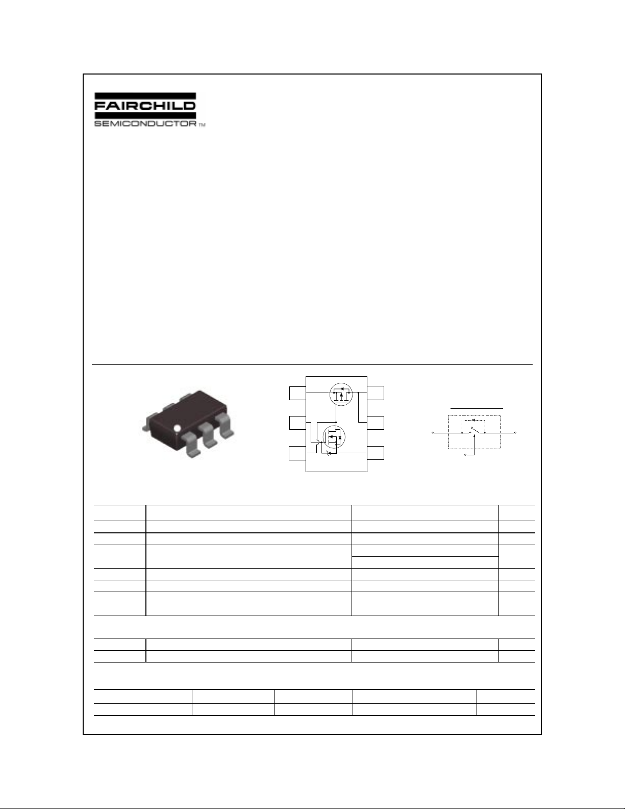
This device is particularly suited for compact power
management in portable electronic equipment where 3V
to 20V input and 2.3A output current capability are needed.
This load switch integrates a small N-Channel power
MOSFET (Q1) which drives a large P-Channel power
MOSFET (Q2) in one tiny SuperSOTTM-6 package.
Applications
• Power management
• Load actuation
Vin,R1
ON/OFF
R1,C1
SuperSOT -6
TM
Features
• V
= 0.2V @ VIN = 12V, IL=2.5 A. R
DROP
V
= 0.2V @ VIN= 5V,IL= 1.6 A. R
DROP
= 0.08 Ω
(ON)
= 0.125 Ω.
(ON)
• Control MOSFET (Q1) includes Zener protection for
ESD ruggedness (>6kV Human Body Model).
• High performance PowerTrenchTM technology for
extremely low on-resistance.
• SuperSOTTM-6 package design using copper lead frame
for superior thermal and electrical capabilities.
Vout,C1
Q1
3
EQUIVALE N T CIRCUIT
Vout,C1
2
IN
1
R2
ON/OFF
V
DRO P
+
4
Q2
5
6
Se e A pplic at ion Cir cu it
-
OUT
T
=25oC unless otherwise noted
Absolute Maximum Ratings
A
Symbol Parameter Ratings Units
V
IN
V
ON/OFF
I
D
Input Voltage Range
On/Off Voltage Range 1.5 - 8 V
Load Current - Continuous
- Pulsed 10
P
D
TJ, T
stg
Max im um Power D is sip ation
Operating and Storage Temperature Range -55 to +150
ESD Electro sta tic D is c ha rge Rating MIL-STD-883D
Human-Bod
-Model (100pf/1500 Ohm
(Note 1)
Note 2
(Note 1)
3 - 20 V
2.3 A
0.7 W
6kV
Thermal Characteristics
R
JA
θ
R
JC
θ
Thermal Resistance, Junction-to-Ambient
Thermal Resistance, Junction-to-Case
(Note 2)
(Note 2)
180
60
Package Marking and Ordering Information
Device Marking Device Reel Size Tape width
330 (
Denotes pin 1)
.
.
1999 Fairchild Semiconductor Corporation
FDC6330L 7’’ 8m m 3000 units
°
C/W
°
C/W
°
Qua ntity
FDC6330L Rev. C
C
Page 2
FDC6330L
Electrical Characteristics
TA=25oC unless otherwise noted
Symbol Parameter Test Conditions Min Typ Max Units
OFF Characteristics
I
FL
ON Characteristics
DROP
R
(ON)
L
Notes:
1. Range of Vin can be up to 30V, but R1 and R2 must be scaled such that VGS of Q2 does not exceed 20V.
2. R
surface of the drain pins. R
3. Pulse Test: Pulse Width < 300µs, Duty Cycle < 2.0%.
Leakage Current VIN = 20 V, V
(Note 3)
V
Conduction Voltage
IN
V
IN
= 12 V, V
= 5 V, V
Q2 - Static On-Resist ance VGS = -12 V, ID = -2.3 A
V
= -5 V, ID = -1.9 A
GS
V
Load Current
is the sum of the junction-to-case and case-to-ambient thermal resistance where the case thermal reference is defined as the solder mounting
θJA
is guaranteed by design while R
θJC
= 0.2 V, VIN = 12 V, V
DROP
= 0.2 V, VIN = 5 V, V
V
DROP
= 250 µA1
ON/OFF
= 3.3 V, IL = 2.5 A 0.2 V V
ON/OFF
= 3.3 V, IL = 1.6 A 0.2 V
ON/OFF
= 3.3 V 2.5 I
ON/OFF
= 3.3 V 1.6
ON/OFF
is determined by the user’s board design.
θJA
0.054
0.081
0.08
0.125
µ
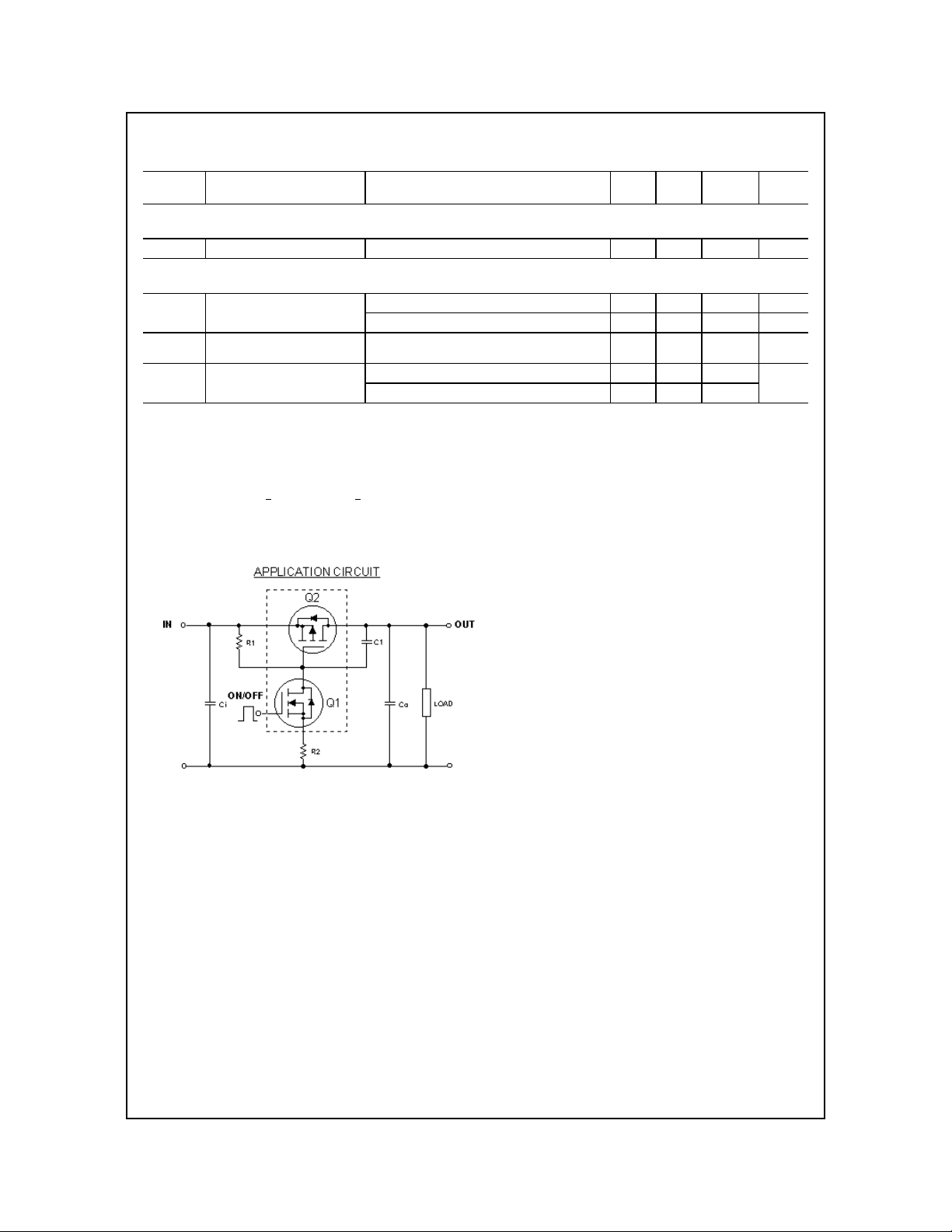
FDC6330L Load Switch Application
A
Ω
A
External Component Recommendation:
For applications where Co ≤ 1µF.
For slew rate control, select R2 in the range of 1k - 4.7kΩ .
For additional in-rush current control,C1 ≤ 1000pF can be added.
Select R1 so that the R1/R2 ratio ranges from 10 - 100. R1 is required to turn Q2 off.
FDC6330L Rev. C
Page 3
T ypical Characteristics (continued)
FDC6330L
0.4
0.3
0.2
DROP
V (V)
0.1
0
012345
I , (A)
L
T = 125°C
J
T = 25°C
J
V = 12V
IN
V = 1. 5 - 8 V
ON/OF F
PW =300 us, D≤ 2%
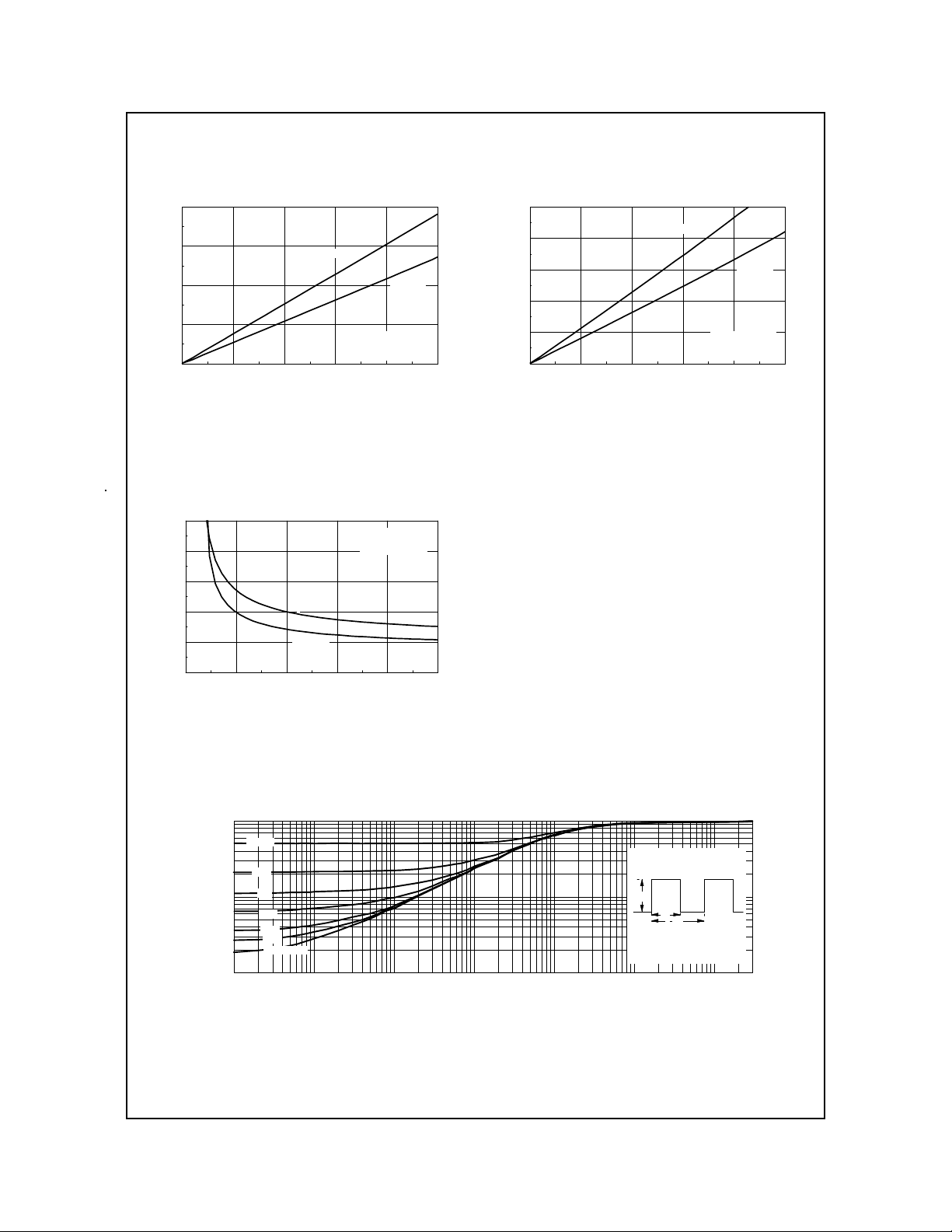
Figure 1. Conduction Voltage Drop
Variation with Load Current.
0.25
0.2
0.15
T = 125°C
0.1
(O N)
R ,(Ohm)
0.05
0
24681012
J
T = 25°C
J
V , (V)
IN
I = 1 A
L
V = 1.5 - 8V
ON/OFF
PW =30 0us, D≤ 2%
0.5
T = 125°C
I , (A)
L
J
T = 25°C
J
V = 5 V
IN
V = 1. 5 - 8 V
ON/OF F
PW =300 us, D≤ 2%
0.4
0.3
DROP
0.2
V (V)
0.1
0
012345
Figure 2. Conduction V oltage Drop
Variation with Load Current.
Figure 3. On-Resistance Variation
with Input Voltage.
1
D = 0.5
0.5
0.2
0.2
0.1
0.1
0.05
0.05
0.02
r(t), NORMALIZED EFFECTIVE
0.02
TRANSIENT THERMAL RESISTANCE
0.01
0.01
Single Pulse
0.0001 0.001 0.01 0.1 1 10 100 300
t , TIME (sec)
1
R (t) = r(t) * R
JA
θ
R =
180
JA
θ
P(pk)
t
1
t
2
T - T = P * R (t)
J
A
Duty Cycle, D = t / t
Figure 4.Transient Thermal Response Curve.
Thermal characterization performed using the conditions described in Note 2.
Transient themal response will change depending on the circuit board design.
°C/W
JA
θ
JA
θ
2
1
FDC6330L Rev. C
Page 4
TRADEMARKS
The following are registered and unregistered trademarks Fairchild Semiconductor owns or is authorized to use and is
not intended to be an exhaustive list of all such trademarks.
ACEx™
CoolFET™
CROSSVOLT™
E2CMOS
TM
FACT™
FACT Quiet Series™
®
FAST
FASTr™
GTO™
HiSeC™
ISOPLANAR™
MICROWIRE™
POP™
PowerTrench™
QS™
Quiet Series™
SuperSOT™-3
SuperSOT™-6
SuperSOT™-8
TinyLogic™
DISCLAIMER
FAIRCHILD SEMICONDUCTOR RESERVES THE RIGHT TO MAKE CHANGES WITHOUT FURTHER
NOTICE TO ANY PRODUCTS HEREIN TO IMPROVE RELIABILITY, FUNCTION OR DESIGN. FAIRCHILD
DOES NOT ASSUME ANY LIABILITY ARISING OUT OF THE APPLICATION OR USE OF ANY PRODUCT
OR CIRCUIT DESCRIBED HEREIN; NEITHER DOES IT CONVEY ANY LICENSE UNDER ITS PATENT
RIGHTS, NOR THE RIGHTS OF OTHERS.
LIFE SUPPORT POLICY
FAIRCHILD’S PRODUCTS ARE NOT AUTHORIZED FOR USE AS CRITICAL COMPONENTS IN LIFE SUPPORT
DEVICES OR SYSTEMS WITHOUT THE EXPRESS WRITTEN APPROVAL OF FAIRCHILD SEMICONDUCTOR CORPORATION.
As used herein:
1. Life support devices or systems are devices or
systems which, (a) are intended for surgical implant into
the body, or (b) support or sustain life, or (c) whose
failure to perform when properly used in accordance
with instructions for use provided in the labeling, can be
reasonably expected to result in significant injury to the
user.
2. A critical component is any component of a life
support device or system whose failure to perform can
be reasonably expected to cause the failure of the life
support device or system, or to affect its safety or
effectiveness.
PRODUCT STATUS DEFINITIONS
Definition of Terms
Datasheet Identification Product Status Definition
Advance Information
Preliminary
No Identification Needed
Obsolete
Formative or
In Design
First Production
Full Production
Not In Production
This datasheet contains the design specifications for
product development. Specifications may change in
any manner without notice.
This datasheet contains preliminary data, and
supplementary data will be published at a later date.
Fairchild Semiconductor reserves the right to make
changes at any time without notice in order to improve
design.
This datasheet contains final specifications. Fairchild
Semiconductor reserves the right to make changes at
any time without notice in order to improve design.
This datasheet contains specifications on a product
that has been discontinued by Fairchild semiconductor.
The datasheet is printed for reference information only.
 Loading...