

Page 1
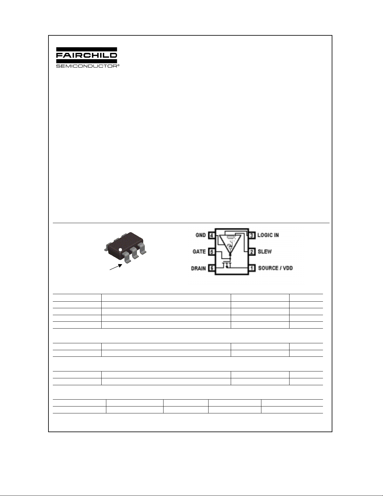
FDC6901L
Integrated Load Switch
General Description
This device is particularly suited for compact power
management. In portabl e electronic equipm ent where 2.5V
to 6V input capability is needed. This load switch integrates
a Slew Rate Control Driver that drives a P-Channel Power
MOSFET in one tiny SuperSOT-6 package. The
integrated slew rate cont rol driver is specifically designed
to control the turn on of the P-Channel MOSFET in order to
limit the inrush current in battery switching applications with
high capacitance loads. For turn-off, the IC pulls the
MOSFET gate up quickly.
Applications
• Load switch
• Power management
D2
S1
D1
May 2002
Features
• Three programmable slew rates
• Reduces inrush current
• Minimizes EMI
• Normal turn-off speed
• Low-power CMOS operates over wide voltage range
• High performance trench te chnology for extremely
low R
DS(ON)
FDC6901L
G2
G1
S2
=25oC unless otherwise noted
A
SuperSOT -6
TM
Pin 1
SuperSOT™-6
Absolute Maximum Ratings T
Symbol Parameter Ratings Units
VDD Supply Voltage –0.5 to 10 V
VIN DC Input Voltage (Logic Inputs) –0.7 to 6 V
PD Power Dissipation
T
Storage Junction Temperat ure Range –55 to +150 °C
STG
Recommended Operating Range
VDD Supply Voltage –0.5 to 10 V
TJ Operating Junction Temperat ure –55 to +150 °C
Thermal Characteristics
R
θJA
R
θJC
Thermal Resistance, Junction to Ambient 180 °C/W
Thermal Resistance, Junction to Case 60 °C/W
Package Marking and Ordering Information
Device Marking Device Reel Size Tape Width Quantity
.901 FDC6901L 7” 8mm 3000 units
2002 Fairchild Semiconductor Corporation
FDC6901L Rev C (W)
Page 2
µ
µ
Electrical Characteristics T
=25oC unless otherwise noted
A
FDC6901L
Symbol Parameter Test Conditions Min Typ Max Units
Logic Levels
VIH Logi c HIGH Input Voltage VDD = 2.7 V to 6.0 V
VIL Logic LOW Input Voltage VDD = 2.7 V to 6.0 V
75%*
V
DD
25%*
V
V
DD
V
OFF Characteristics – Slew Rate Control Driver
BVDG Supply Input Breakdown Voltage I
BV
Sl ew Input Breakdown Voltage I
SLEW
BVIN Logic Input Breakdown Voltage I
IRDG Supply Input Leakage Current V
IR
Slew Input Leakage Current V
SLEW
IRIN Logic Input Leakage Current V
= 10 µA, V
DG
= 10 µA, V
SLEW
= 10 µA, V
IN
= 8 V, V
DG
= 8 V, V
SLEW
= 8 V, V
IN
= 0 V, V
IN
= 0 V 9 V
IN
= 0 V 9 V
SLEW
= 0 V, V
IN
= 0 V 100 nA
IN
= 0 V 100 nA
SLEW
= 0 V 9 V
SLEW
= 0 V 100 nA
SLEW
OFF Characteristics – Slew Rate Control Driver + P-Channel MOSFET
BVIO IO Breakdown Voltage
I
= –250 µA
D
IRIO IO Leakage Current VR = 16 V 100 nA
9 V
ON Characteristics – Slew Rate Control Driver
IG Output/Gate Current VIN = 6V
= 2V
V
GATE
Slew Pin = OPEN
= GROUND
= V
DD
90
1
10
µA
µA
nA
ON Characteristics – P-Channel MOSFET
V
Gate Threshold Voltage
GS(th)
R
Stat i c Drain-Source On
DS(ON)
Resistance
V
= VGS , ID = –250 µA
DS
V
= –4.5 V, ID = –1.5 A
GS
= –2.5 V, ID = –1.2 A
V
GS
–0.6 –1.0 –1.5 V
120
170
145
210
mΩ
mΩ
ON Characteristics – Slew Rate Control Driver + P-Channel MOSFET
V
Dropout Voltage VDD = 6V, VIN = 2.5V to 6V, IL = 1.5 A
DROP
= 6V, VIN = 2.5V to 6V, IL = 1.2 A
V
DD
RON Load switch On Resistance VDD = 6V, VIN = 2.5V to 6V, IL = 1.5 A
= 6V, VIN = 2.5V to 6V, IL = 1.2 A
V
DD
I
Load Current
LOAD
V
= 2.5 V, VDS = 6 V
GS
160
130
105
110
3 A
300
300
180
210
mV
mV
mΩ
mΩ
P-Channel MOSFET Switching Times
Vsupply = 5.5V, VDD = 5.5V, Logic IN = 5.5V, I
Output Turn-On Delay Ti me S l ew Pin = OP E N
t
don
t
Output Rise Time Slew Pin = OPEN
rise
dv/dt Output Slew Rate Slew Pin = OPEN
= 1.5A
LOAD
= GROUND
= V
DD
= GROUND
= V
DD
= GROUND
= V
DD
6.20
42
115
6.75
124
162
600
41
24
µs
µs
s
µs
µs
s
V/ms
V/ms
V/ms
FDC6901L Rev C (W)
Page 3

Typical Characteristics
FDC6901L
220
VDD = 6V
= 2.55V to 6V
V
IN
200
180
160
140
120
Dropout Voltage, VDrop (mV)
100
-50 -25 0 25 50 75 100 125 150
Junction Temperature, oC
IL = 1.5A
IL = 1.2A
Figure 1. Dropout Voltage vs. Temperature.
SLEW = OPEN
200
180
160
140
120
Dropout Voltage, VDrop (mV)
TJ = 125oC
TJ = 25oC
450
VDD = 6V
= 2.55V to 6V
V
IN
400
350
300
250
200
150
100
Dropout Voltage, VDrop (mV)
50
0
0123
TJ = 125oC
TJ = 25oC
Load Current, Amps (A)
Figure 2. Dropout Voltage vs. Load Current.
SLEW = OPEN
(mΩ)
ON
On-Resistance, R
140
VDD = 6V
= 2.55V to 6V
V
IN
130
120
110
100
90
IL = 1.2A
IL = 1.5A
I
= 1A
LOAD
100
2.5 3 3.5 4 4.5
Input Voltage, VDD (V)
Figure 3. Dropout Voltage vs. Input Voltage.
SLEW = OPEN
10
VDD = 6V
= 2.55V to 6V
V
IN
)
Ω
(
1
ON
TJ = 125oC
0.1
On Resistance, R
0.01
0.01 0.1 1 10
TJ = 25oC
Load Current, Amps (A)
Figure 5. On-Resistance vs. Load Current.
SLEW = OPEN
80
-50 -25 0 25 50 75 100 125 150
Junction Temperature, oC
Figure 4. On-Resistance vs. Temperature.
SLEW = OPEN
200
180
)
Ω
(m
ON
160
140
On-Resistance, R
120
100
2.533.544.5
Input Voltage, VDD (V)
TJ = 125oC
TJ = 25oC
I
LOAD
Figure 6. . On-Resistance vs. Input Voltage.
SLEW = OPEN
= 1A
FDC6901L Rev C (W)
Page 4

trise
0
Typical Characteristics
FDC6901L
7.5
7.0
s)
µ
6.5
6.0
time, microseconds (
5.5
5.0
0 102030405
trise
tdon
Load Resistance, ohms (Ω)
Slew = Open
Vdd=Vin=5.5V
Figure 7. Switching Time vs. Load
Resistance. SLEW = OPEN
200
175
s)
µ
150
125
time, microseconds (
100
tris
tdon
Slew = Vdd
Vdd=Vin=5.5V
160
140
120
100
80
time, µsecs
60
40
20
0
0 1020304050
trise
tdon
Load Resistance, ohms (Ω)
Slew = Gnd
Vdd=Vin=5.5V
Figure 8. Switching Time vs. Load
Resistance. SLEW = GROUND
7.5
Slew = Open
Vdd=Vin=5.5V
7.0
6.5
sec)
µ
6.0
time, (
5.5
trise
tdon
75
0 1020304050
Load Resistance, ohms (Ω)
Figure 9. Switching Time vs. Load
Resistance. SLEW = V
160
Slew = Gnd
Vdd=Vin=5.5V
140
120
100
sec
µ
80
time,
60
40
20
0.0 0.5 1.0 1.5 2.0 2.5
tdon
Load Current, Amps (A)
DD
Figure 11. Switching time vs. Load Current.
SLEW = GROUND
5.0
0.0 0.5 1.0 1.5 2.0 2.5
Load Current, Amps (A)
Figure 10. Switching time vs. Load Current.
SLEW = OPEN
200
Slew = Vdd
Vdd=Vin=5.5V
175
s)
µ
150
125
time, microseconds (
100
75
0.0 0.5 1.0 1.5 2.0 2.5
trise
tdon
Load Current, Amps (A)
Figure 12. Switching time vs. Load Current.
SLEW = VDD
FDC6901L Rev C (W)
Page 5

TRADEMARKS
The following are registered and unregistered trademarks Fairchild Semiconductor owns or is authorized to use and is
not intended to be an exhaustive list of all such trademarks.
ACEx
Bottomless
CoolFET
CROSSVOL T
DenseTrench
DOME
EcoSPARK
E2CMOS
EnSigna
TM
TM
FACT
FACT Quiet Series
STAR*POWER is used under license
FAST
FASTr
FRFET
GlobalOptoisolator
GTO
HiSeC
2
I
C
ISOPLANAR
LittleFET
MicroFET
MicroPak
MICROWIRE
OPTOLOGIC
â
OPTOPLANAR
PACMAN
POP
Power247
PowerTrench
â
QFET
QS
QT Optoelectronics
Quiet Series
SILENT SWITCHER
SMART START
SPM
STAR*POWER
Stealth
SuperSOT-3
SuperSOT-6
SuperSOT-8
SyncFET
TinyLogic
TruTranslation
ââ
UHC
UltraFET
VCX
DISCLAIMER
FAIRCHILD SEMICONDUCTOR RESERVES THE RIGHT TO MAKE CHANGES WITHOUT FURTHER
NOTICE TO ANY PRODUCTS HEREIN TO IMPROVE RELIABILITY, FUNCTION OR DESIGN. FAIRCHILD
DOES NOT ASSUME ANY LIABILITY ARISING OUT OF THE APPLICATION OR USE OF ANY PRODUCT
OR CIRCUIT DESCRIBED HEREIN; NEITHER DOES IT CONVEY ANY LICENSE UNDER ITS PATENT
RIGHTS, NOR THE RIGHTS OF OTHERS.
LIFE SUPPORT POLICY
â
FAIRCHILDS PRODUCTS ARE NOT AUTHORIZED FOR USE AS CRITICAL COMPONENTS IN LIFE SUPPORT
DEVICES OR SYSTEMS WITHOUT THE EXPRESS WRITTEN APPROVAL OF FAIRCHILD SEMICONDUCTOR CORPORATION.
As used herein:
1. Life support devices or systems are devices or
systems which, (a) are intended for surgical implant into
the body, or (b) support or sustain life, or (c) whose
failure to perform when properly used in accordance
with instructions for use provided in the labeling, can be
reasonably expected to result in significant injury to the
user.
PRODUCT STATUS DEFINITIONS
Definition of Terms
Datasheet Identification Product Status Definition
Advance Information
Preliminary
No Identification Needed
Formative or
In Design
First Production
Full Production
2. A critical component is any component of a life
support device or system whose failure to perform can
be reasonably expected to cause the failure of the life
support device or system, or to affect its safety or
effectiveness.
This datasheet contains the design specifications for
product development. Specifications may change in
any manner without notice.
This datasheet contains preliminary data, and
supplementary data will be published at a later date.
Fairchild Semiconductor reserves the right to make
changes at any time without notice in order to improve
design.
This datasheet contains final specifications. Fairchild
Semiconductor reserves the right to make changes at
any time without notice in order to improve design.
Obsolete
Not In Production
This datasheet contains specifications on a product
that has been discontinued by Fairchild semiconductor.
The datasheet is printed for reference information only.
Rev. H5
 Loading...