

Page 1
August 2001
3
2
145
6
Vout,C1
R2Vin,R
1
R1,C1
SeeApplicationCircuit
T
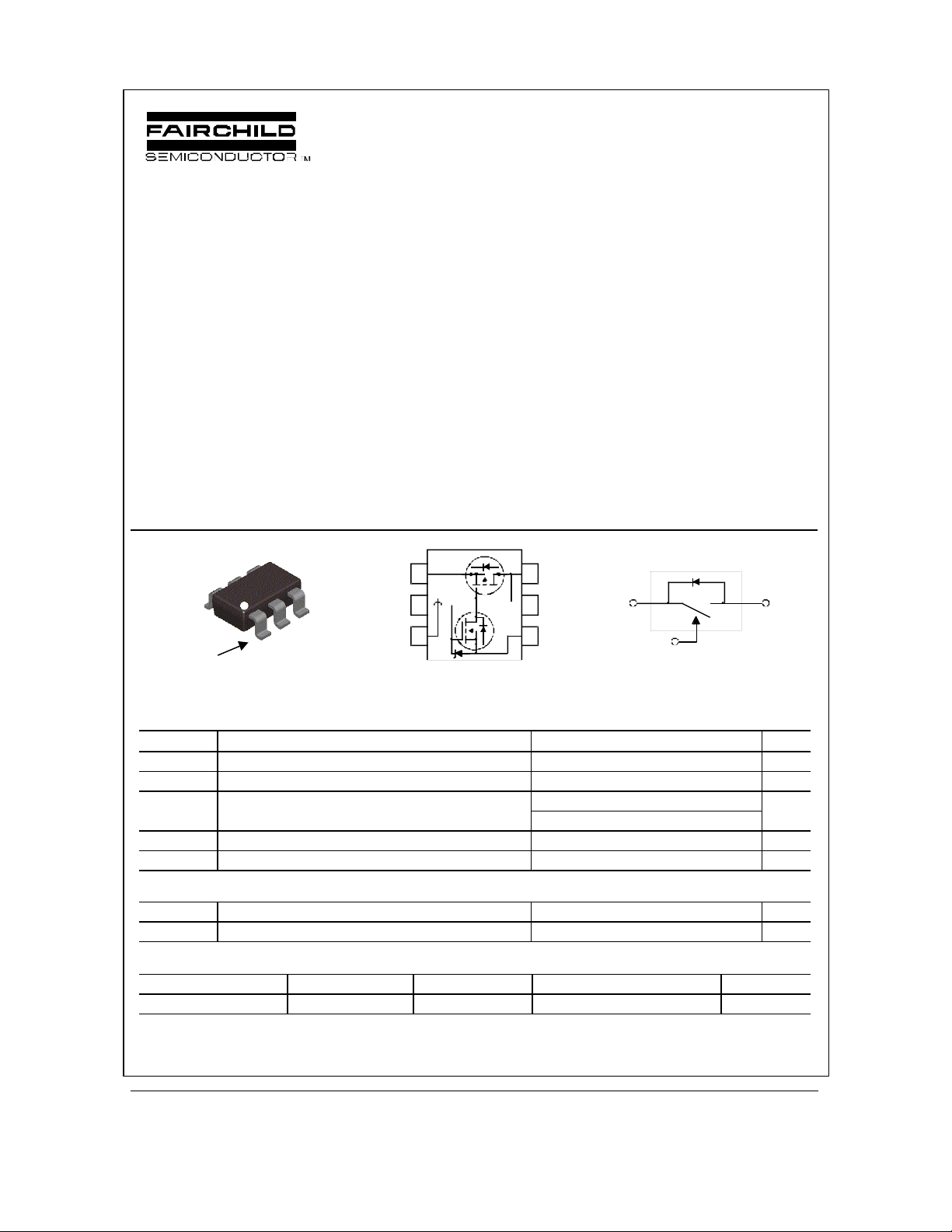
FDC6331L
FDC6331L
Integrated Load Switch
General Description
This device is particularly suited for compact power
management in portable electronic equipment where
2.5V to 8V input and 2.8A output current capability are
Features
• –2.8 A, –8 V. R
R
R
= 55 mΩ @ VGS = –4.5 V
DS(ON)
= 70 mΩ @ VGS = –2.5 V
DS(ON)
= 100 m Ω @ VGS = –1.8 V
DS(ON)
needed. This load switch integrates a s mall N-Channel
power MOSFET (Q1) that drives a large P-Channel
power MOSFET (Q2) in one tiny SuperSOTTM-6
package.
Applications
• Control MOSFET (Q1) includes Zener protection for
ESD ruggedness (>6KV Human body model)
• High performance trench technology for extremely
low R
DS(ON)
• Load switch
• Power management
D2
S1
D1
ON/OFF
G2
G1
S2
SuperSOT -6
TM
Pin 1
SuperSOT™-6
Absolute Maximum Ratings T
o
=25
C unless otherwise noted
A
Q2
Vout,C1
Q1
Equivalent Circuit
+ –IN OU
V
DROP
ON/OFF
Symbol Parameter Ratings Units
VIN Maximum Input Voltage ± 8 V
V
High level ON/OFF voltage range –0.5 to 8 V
ON/OFF
I
Load Current – Continuous (Note 1) –2.8 A
Load
– Pulsed –9
PD Maximum Power Dissipation (Note 1) 0.7 W
TJ, T
Operating and Storage Junction Temperature Range –55 to +150 °C
STG
Thermal Characteristics
R
θJA
R
θJC
Thermal Resistance, Junction-to-Ambient (Note 1) 180
Thermal Resistance, Junction-to-Case (Note 1) 60
°C/W
°C/W
Package Marking and Ordering Information
Device Marking Device Reel Size Tape width Quantity
.331 FDC6331L 7’’ 8mm 3000 units
2001 Fairchild Semiconductor Corporation FDC6331L Rev C(W)
Page 2
FDC6331L
Electrical Characteristics T
= 25°C unless otherw ise noted
A
Symbol Parameter Test Conditions Min Typ Max Units
Off Characteristics
BVIN Vin Breakdown Voltage V
I
Zero Gate Voltage Drain Current VIN = 6.4 V, V
Load
IFL Leakage Current, Forward V
IRL Leakage Current, Reverse V
= 0 V, ID = –250 µA 8 V
ON/OFF
= 0 V –1 µA
ON/OFF
= 0 V, VIN = 8 V –100 nA
ON/OFF
= 0 V, VIN = –8 V 100 nA
ON/OFF
On Characteristics (Note 2)
V
R
R
Gate Threshold Voltage VIN = V
ON/OFF (th)
Static Drain–Source
DS(on)
On–Resistance (Q2)
Static Drain–Source
DS(on)
On–Resistance (Q1)
, ID = –250 µA 0.4 0.9 1.5 V
ON/OFF
VIN = 4.5 V, ID = –2.8A
VIN = 2.5 V, ID = –2.5 A
VIN = 1.8 V, ID = –2.0 A
VIN = 4.5 V, ID = 0.4A
VIN = 2.7 V, ID = 0.2 A
34
45
64
3.1
3.8
55
70
100
4
5
m Ω
Drain–Source Diode Characteristics and Maximum Ratings
IS Maximum Continuous Drain–Source Diode Forward Current –0.6 A
VSD Drain–Source Diode Forward
V
= 0 V, IS = –0.6 A (Note 2) –1.2 V
ON/OFF
Voltage
Notes:
1. R
is the sum of the junction-to-case and case-to-ambient thermal resistance where the case thermal reference is defined as the solder mounting
θJA
surface of the drain pins. R
2. Pulse Test: Pulse Width < 300µs, Duty Cycle < 2.0%.
is guaranteed by design while R
θJC
is determined by the user’s board design.
θJA
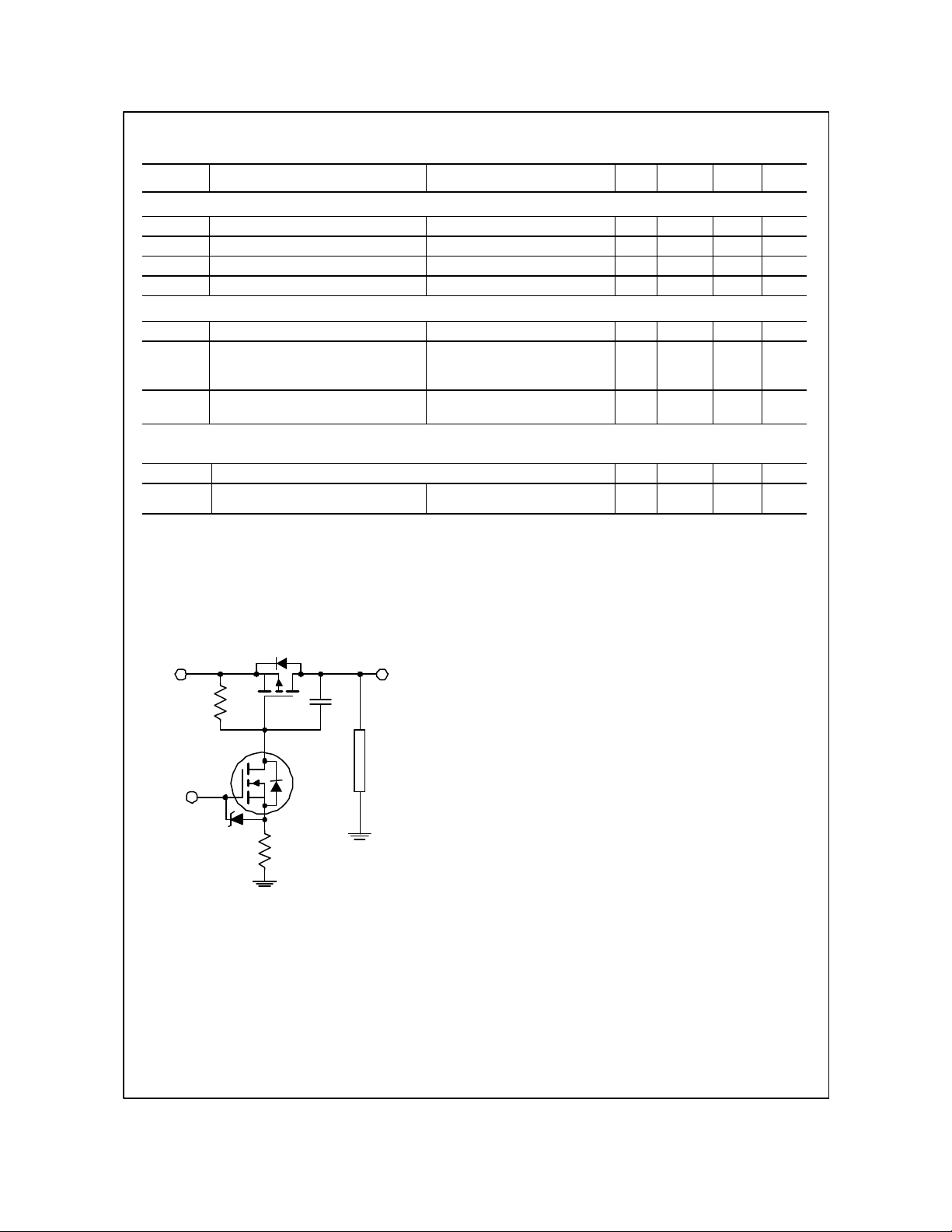
FDC6331L Load Switch Application Circuit
IN
Q2
OUT
Ω
R1
C1
Q1
LOAD
ON/OFF
R2
External Component Recommendation:
For additional in-rush current control, R2 and C1 can be added. For more information, see application note AN1030.
FDC6331L Rev C(W)
Page 3

P(pk)
0.02
0.05
FDC6331L
0.4
VIN = -1.8V
0.35
V
= -1.5V -8V
ON/OFF
PW = 300us, D < 2%
0.3
0.25
, (V)
0.2
DROP
-V
0.15
0.1
0.05
0
0 1 2 3 4 5 6
TJ = 125OC
TJ = 25OC
-IL, (A)
Figure 1. Conduction Voltage Drop
Variation with Load Current.
0.4
VIN = -4.5V
0.35
V
= -1.5V -8V
ON/OFF
PW = 300us, D < 2%
0.3
0.25
, (V)
0.2
DROP
-V
0.15
0.1
0.05
0
0 1 2 3 4 5 6
TJ = 125OC
-IL, (A)
Figure 3. Conduction Voltage Drop
Variation with Load Current.
TJ = 25OC
0.4
VIN = -2.5V
V
0.35
0.3
0.25
, (V)
0.2
DROP
-V
0.15
0.1
0.05
= -1.5V -8V
ON/OFF
PW = 300us, D < 2%
TJ = 125OC
TJ = 25OC
0
0 1 2 3 4 5 6
-IL, (A)
Figure 2. Conduction Voltage Drop
Variation with Load Current.
0.15
0.125
0.1
0.075
0.05
RDS(ON) , ON-RESISTANCE ( )
0.025
0
TJ = 25OC
1 2 3 4 5
-VIN, INPUT VOLTAGE (V)
TJ = 125OC
IL = -1A
V
= -1.5V -8V
ON/OFF
PW = 300us, D < 2%
Figure 4. On-Resistance Variation
With Input Voltage
1
0.1
D = 0.5
0.2
0.1
R
JA(t) = r(t) + RθJA
θ
R
JA = 156 °C/W
θ
t1
t2
TJ - TA = P * R
(t)
θJA
Duty Cycle, D = t1 / t2
r(t), NORMALIZED EFFECTIVE
TRANSIENT THERMAL RESISTANCE
0.01
0.01
SINGLE PULSE
0.0001 0.001 0.01 0.1 1 10 100 1000
FDC6331L Rev C(W)
Page 4

TRADEMARKS
The following are registered and unregistered trademarks Fairchild Semiconductor owns or is authorized to use and is
not intended to be an exhaustive list of all such trademarks.
ACEx™
Bottomless™
CoolFET™
CROSSVOLT™
DenseTrench™
DOME™
EcoSPARK™
E2CMOS
EnSigna
TM
TM
FACT™
FACT Quiet Series™
STAR*POWER is used under license
FAST
FASTr™
FRFET™
GlobalOptoisolator™
GTO™
HiSeC™
ISOPLANAR™
LittleFET™
MicroFET™
MicroPak™
MICROWIRE™
OPTOLOGIC™
OPTOPLANAR™
PACMAN™
POP™
Power247™
PowerTrench
QFET™
QS™
QT Optoelectronics™
Quiet Series™
SILENT SWITCHER
SMART START™
STAR*POWER™
Stealth™
SuperSOT™-3
SuperSOT™-6
SuperSOT™-8
SyncFET™
TinyLogic™
TruTranslation™
UHC™
UltraFET
VCX™
DISCLAIMER
FAIRCHILD SEMICONDUCTOR RESERVES THE RIGHT TO MAKE CHANGES WITHOUT FURTHER
NOTICE TO ANY PRODUCTS HEREIN TO IMPROVE RELIABILITY, FUNCTION OR DESIGN. FAIRCHILD
DOES NOT ASSUME ANY LIABILITY ARISING OUT OF THE APPLICATION OR USE OF ANY PRODUCT
OR CIRCUIT DESCRIBED HEREIN; NEITHER DOES IT CONVEY ANY LICENSE UNDER ITS PATENT
RIGHTS, NOR THE RIGHTS OF OTHERS.
LIFE SUPPORT POLICY
FAIRCHILD’S PRODUCTS ARE NOT AUTHORIZED FOR USE AS CRITICAL COMPONENTS IN LIFE SUPPORT
DEVICES OR SYSTEMS WITHOUT THE EXPRESS WRITTEN APPROVAL OF FAIRCHILD SEMICONDUCTOR CORPORATION.
As used herein:
1. Life support devices or systems are devices or
systems which, (a) are intended for surgical implant into
the body, or (b) support or sustain life, or (c) whose
failure to perform when properly used in accordance
with instructions for use provided in the labeling, can be
reasonably expected to result in significant injury to the
user.
PRODUCT STATUS DEFINITIONS
Definition of Terms
Datasheet Identification Product Status Definition
Advance Information
Preliminary
No Identification Needed
Formative or
In Design
First Production
Full Production
2. A critical component is any component of a life
support device or system whose failure to perform can
be reasonably expected to cause the failure of the life
support device or system, or to affect its safety or
effectiveness.
This datasheet contains the design specifications for
product development. Specifications may change in
any manner without notice.
This datasheet contains preliminary data, and
supplementary data will be published at a later date.
Fairchild Semiconductor reserves the right to make
changes at any time without notice in order to improve
design.
This datasheet contains final specifications. Fairchild
Semiconductor reserves the right to make changes at
any time without notice in order to improve design.
Obsolete
Not In Production
This datasheet contains specifications on a product
that has been discontinued by Fairchild semiconductor.
The datasheet is printed for reference information only.
Rev. H4
 Loading...