

Page 1
www.fairchildsemi.com
FAN1537
Dual 1A Adjustable/Fixed Low Dropout
Linear Regulators
Features
• Low dropout voltage
• Load regulation: 0.05% typical
• On-chip thermal limiting
• SO-8 and 5-lead SPAK and TO-252 DPAK packages
• Fixed 3.3V, and adjustable or 2.5V or 1.8V fixed
• Stable with low ESR output capacitors
Applications
• Hard Disk Drives, CD-ROMs, DVDs
• High efficiency linear regulators
• Post regulators for switching supplies
• ADSL and Cable Modems
• 5V to 3.3V and 2.5V linear regulators
• Motherboard with multiple supplies
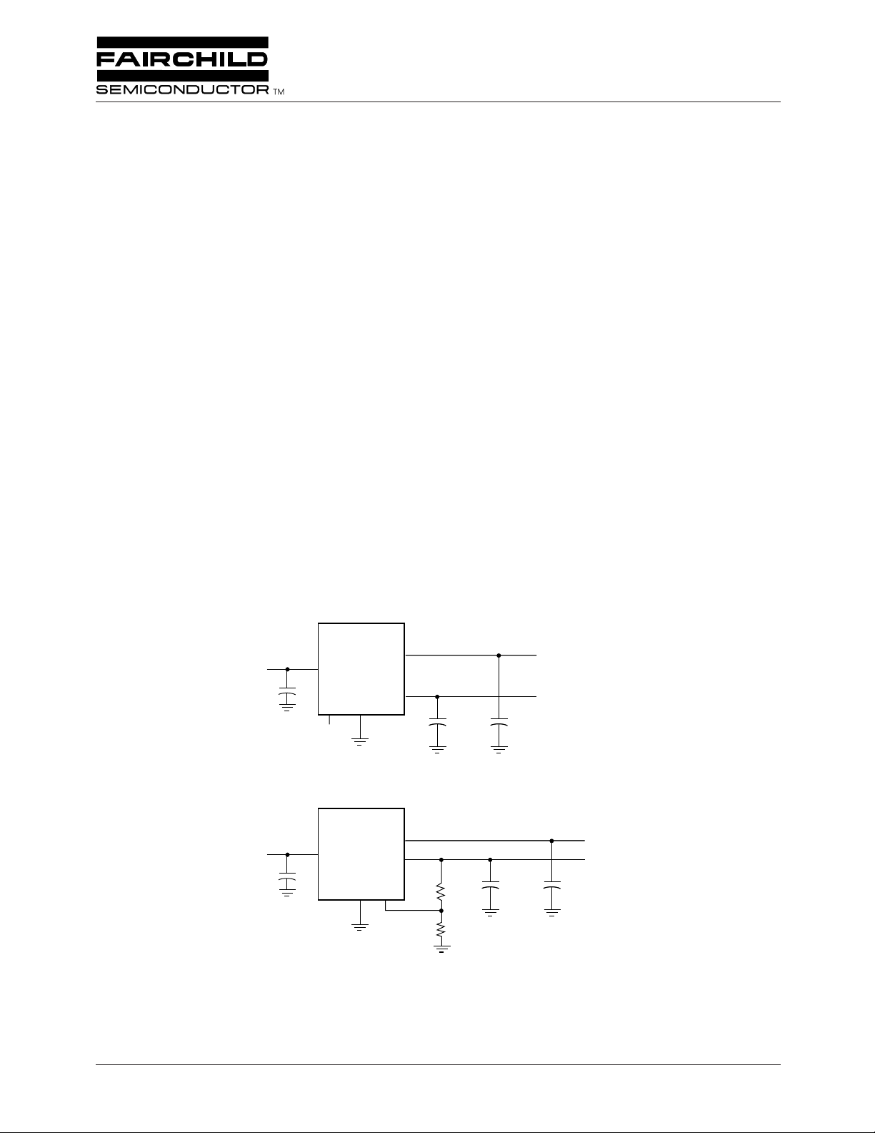
Typical Applications
FAN1537A
V
IN
= 5V
22µF
V
IN
+
GND
NC
V1
V2
Description
The FAN1537 provides 2 output voltages: 3.3V, and either
adjustable or 2.5V or 1.8V fixed with 1.0A each output
current capability. These devices have been optimized for
low voltage where transient response and minimum input
voltage are critical.
Current limit features protect the outputs against short circuit
currents. On-chip thermal limiting provides protection
against any combination of overload and ambient temperature that would create excessive junction temperatures.
The FAN1537 series regulators are available in SO-8 and
5-lead SPAK and TO-252 DPAK power packages.
3.3V at 1.0A
3.3V at 1.0A
2.5V at 1.0A
2.5V at 1.0A
+
+
22µF
22µF
+
+
22µF
22µF
FAN1537B
V
IN
= 5V
22µF
V
IN
+
V1
V2
GND FB
V2 = V
(1 + R1/R2)
REF
R1
54.9Ω
R2
124Ω
+
+
22µF
22µF
+
+
22µF
22µF
3.3V at 1.0A
3.3V at 1.0A
1.8V at 1.0A
REV. 1.1.1 3/20/02
Page 2
FAN1537 PRODUCT SPECIFICATION
Pin Assignments
V
NC
1
IN
2
V1
3
V2
4
8-Lead Plastic SO-8
TOP VIEW
Θ
=25°C/W
JC
FAN1537PA
FAN1537PC
FRONT VIEW
GND
8
GND
7
GND
6
GND
5
12345
IN
V
5-Lead SPAK
Θ
JC
NC
GND
=2°C/W
V1
V2
FAN1537PB
FRONT VIEW
12345
IN
FB
GND
=2°C/W
V2
V
5-Lead SPAK
Θ
JC
V1
FAN1537DA
FAN1537DC
FRONT VIEW
12345 12345
IN
V
V1
NC
GND
5-Lead Plastic TO-252 DPAK
=3°C/W Tab is GND
Θ
JC
Pin Descriptions
SPAK
Pin Name SO-8
V
IN
1 1 Input supply voltage
NC/FB 2 2 For V2 fixed, no connect. For V2 adjustable, feedback voltage.
V1 3 4/5 Output #1
V2 4 5/4 Output #2
GND 5, 6, 7, 8 3 Ground
DPAK Pin Function
V2
FAN1537DB
FRONT VIEW
IN
FB
V
GND
V2
V1
Absolute Maximum Ratings
Parameter Min. Max. Unit
V
IN
Operating Junction Temperature Range 0 150 °C
Storage Temperature Range -65 150 °C
Lead Temperature (Soldering, 10 sec.) 300 °C
10 V
2
REV. 1.1.1 3/20/02
Page 3
≤
≤
≤
•
≥
≤
≤
•
≤
•
≤
•
∆
•
•
≤
•
•
PRODUCT SPECIFICATION FAN1537
Electrical Characteristics
(Operating Conditions: V
IN
7V, T
=25°C unless otherwise specified.)
J
The • denotes specifications which apply over the specified operating temperature range of 0°C to 125°C junction temperature.
Parameter Conditions Min. Typ. Max. Units
Output Voltages 10mA ≤ I
4.75V ≤ V
Output Voltage 3.3V Output, V
Time to Output Voltages Valid From V
Reference Voltage, V
REF
10mA ≤ I
IN
4.75V ≤ V
Line Regulation
1,2
4.75V ≤ V
1A
OUT
IN
7V
= 4.5V, I
IN
OUT
= 1A
•
•
•
1.764
1.742
2.450
2.420
3.234
3.200
1.8
1.8
2.500
2.500
3.300
3.300
3.2 V
1.836
1.858
2.550
2.580
3.366
3.400
4.75V 5 msec
OUT
IN
IN
1A
7V
7V, I
OUT
= 10mA
1.225
1.210
1.250
1.250
1.275
1.290
0.005 0.5 %
V
V
(both outputs)
Load Regulation
1,2
V
= 4.75V, 10mA ≤ I
IN
OUT
1A
0.05 0.5 %
(both outputs)
Dropout Voltage
V
OUT
= 1%, I
OUT
= 1A
1.100 1.300 V
(3.3V output)
Current Limit
V
IN
= 5V
1.3 1.5 A
(both outputs)
Minimum Load Current
4.75V ≤ V
IN
7V
10 mA
(both outputs)
Quiescent Current V
Ripple Rejection
3
(both outputs)
Long-Term Stability T
RMS Output Noise (% of V
OUT
Thermal Resistance, Junction to
Case
Thermal Shutdown
Thermal Shutdown Hysteresis Junction Temperature
Notes:
1. See thermal regulation specifications for changes in output voltage due to heating effects. Load and line regulation are
measured at a constant junction temperature by low duty cycle pulse testing.
2. Power dissipation is determined by input/output differential and the output current. Guaranteed maximum output power will
not be available over the full input/output voltage range.
3. ESR = 0.2 Ω .
4. For adjust only, V
OUT
= V
(1 + R1/R2)
REF
= 7V
IN
f = 120Hz, C
V
= 5V, I
IN
= 125°C, 1000 hrs.
A
)T
= 25°C, 10Hz ≤ f ≤ 10kHz
A
OUT
OUT
= 1A
SO-8
= 22µF Tantalum,
615mA
60 dB
0.03 1.0 %
0.003 %
50 °C/W
TO-252 DPAK 3 °C/W
SPAK
2 °C/W
155 °C
10 °C
REV. 1.1.1 3/20/02
3
Page 4

FAN1537 PRODUCT SPECIFICATION
Application Hints
External Capacitors
Like any low-dropout regulator, the FAN1537 requires
external capacitors for stability.
Input Capacitor
A Tantalum input capacitor of 22µF is recommended. This
capacitor must be located at a distance of no more than 0.5"
from the input pin of the device and returned to a clean analog ground.
Output Capacitor
The FAN1537 is designed to work with Ceramic or Tantalum
load capacitors.
A value of 22µF is recommended on each output, but the
value can be reduced to 10µF to save space.
Additional capacitance can be added without limit for better
performance, e.g. improved transient response and lower
noise.
When a Ceramic multilayer capacitor is used, the X7R
dielectric is recommended which holds the capacitance
within ±15%. The output capacitor should be located not
more than 0.5" from the output pins of the device and
returned to a clean analog ground.
4
REV. 1.1.1 3/20/02
Page 5

PRODUCT SPECIFICATION FAN1537
Mechanical Dimensions
8-Lead SOIC Package
Symbol
A .053 .069 1.35 1.75
A1 .004 .010 0.10 0.25
B .013 0.33
C .0075 .010 0.20 0.25
D .189 .197 4.80 5.00
E .150 .158 3.81 4.01
e
H
h
L .016 .050 0.40 1.27
N8 8
α
ccc .004 0.10——
85
Inches
Min. Max. Min. Max.
.020 0.51
.050 BSC 1.27 BSC
.228 .244 5.79 6.20
.010 .020 0.25 0.50
0° 8° 0° 8°
EH
Millimeters
Notes
Notes:
1.
Dimensioning and tolerancing per ANSI Y14.5M-1982.
2.
"D" and "E" do not include mold flash. Mold flash or
protrusions shall not exceed .010 inch (0.25mm).
3.
"L" is the length of terminal for soldering to a substrate.
4.
5
2
2
3
6
Terminal numbers are shown for reference only.
5.
"C" dimension does not include solder finish thickness.
6.
Symbol "N" is the maximum number of terminals.
14
D
A
e
B
A1
SEATING
PLANE
– C –
LEAD COPLANARITY
ccc C
h x 45°
C
α
L
REV. 1.1.1 3/20/02
5
Page 6

FAN1537 PRODUCT SPECIFICATION
Mechanical Dimensions
5-Lead SPAK
Symbol
A 0.3600.350
B
b1
b2
C 0.080
c1 0.0500.040
c2
D
E
e
L 0.4200.410
L1
L2
L3
R
α
Inches
Min. Max. Min. Max.
0.220 NOM
0.268
0.0310.025
0.070
0.010 NOM
0.295 NOM
0.3750.365 9.529.27
0.067
0.0410.031 1.040.79
0.3600.350 9.148.89
0.3200.310 8.137.87
0.010 NOM 0.25 NOM
0° 8°
Millimeters
5.59 NOM
6.81
1.78
0.25 NOM
7.49 NOM
1.72
0° 8°
9.148.89
0.790.63
2.03
1.271.02
10.6710.41
E
A
B
Notes
Notes:
1. All linear dimensions are in inches (millimeters).
2. This drawing is subject to change without notice.
3. The center lead is in electrical contact with the thermal tab.
4. Dimensions do not include mold protrusions, not to exceed 0.006 (0,15).
C
c1
c2
D
L
51
e
b1
L3
b2
0.010 (0,25)
L2
M
Gage Plane
Thermal Ta b
(See Note 3)
Seating Plane
0.004 (0,10)
0.005 (0.13)
0.001 (0.03)
R
L1
3°–6°
6
REV. 1.1.1 3/20/02
Page 7

FAN1537 PRODUCT SPECIFICATION
Mechanical Dimensions
5-Lead TO-252 Package
0.57±0.07
0.25 M
6.30
5.90
C
(0.44)
6.00 MIN
1.27
3.81
2.40
2.18
B
0.60
0.40
6.56 MIN
3.00 MIN
1.00
5
A
1.27
0.50
1.02
0.60
0.69±0.15
6.25
1
1.27
LAND PATTERN RECOMMENDATION
6.80
6.35
5.64
5.04
3
2
1
MCA
4
1.27
5.08
(5.09)
(4.05)
10.42
9.20
B0.10
GAGE PLANE
0.60
0.40
10°
0°
5
(2.90)
1.78
1.40
SEE
DETAIL A
3
4
2
1
0.51
(1.54)
0.13 MAX
SEATING PLANE
NOTES: UNLESS OTHERWISE SPECIFIED
A) ALL DIMENSIONS ARE IN MILLIMETERS.
B) THIS PACKAGE CONFORMS TO JEDEC, TO-252,
ISSUE C, VARIATION AA, DATED NOV. 1999.
DETAIL A
(ROTATED 90°)
SCALE: 2X
7
REV. 1.1.1 3/20/02
Page 8

FAN1537 PRODUCT SPECIFICATION
Ordering Information
Example: FAN1537PA
FAN1537 AP
M = SO-8
P = SPAK
D = TO-252 DPAK
Table 1.
SuffixV1 V2
A 3.3V 2.5V
B 3.3V ADJ
C 3.3V 1.8V
Table 1
DISCLAIMER
FAIRCHILD SEMICONDUCTOR RESERVES THE RIGHT TO MAKE CHANGES WITHOUT FURTHER NOTICE TO ANY
PRODUCTS HEREIN TO IMPROVE RELIABILITY, FUNCTION OR DESIGN. FAIRCHILD DOES NOT ASSUME ANY
LIABILITY ARISING OUT OF THE APPLICATION OR USE OF ANY PRODUCT OR CIRCUIT DESCRIBED HEREIN; NEITHER
DOES IT CONVEY ANY LICENSE UNDER ITS PATENT RIGHTS, NOR THE RIGHTS OF OTHERS.
LIFE SUPPORT POLICY
FAIRCHILD’S PRODUCTS ARE NOT AUTHORIZED FOR USE AS CRITICAL COMPONENTS IN LIFE SUPPORT DEVICES
OR SYSTEMS WITHOUT THE EXPRESS WRITTEN APPROVAL OF THE PRESIDENT OF FAIRCHILD SEMICONDUCTOR
CORPORATION. As used herein:
1. Life support devices or systems are devices or systems
which, (a) are intended for surgical implant into the body,
or (b) support or sustain life, and (c) whose failure to
perform when properly used in accordance with
instructions for use provided in the labeling, can be
reasonably expected to result in a significant injury of the
user.
www.fairchildsemi.com
2. A critical component in any component of a life support
device or system whose failure to perform can be
reasonably expected to cause the failure of the life support
device or system, or to affect its safety or effectiveness.
3/20/02 0.0m 004
2001 Fairchild Semiconductor Corporation
Stock#DS30001537
 Loading...