

Page 1
FA7622CP(E)
1
FA7622CP(E)
■ Dimensions, mm
Á SSOP-20
1
7.2
10
11
20
5.3
0.6
0~10˚
0.65
7.9
±0.3
0.1
±0.1
0.3
0.2
+
0
.1
–0
.05
2.1max
Á DIP-20
1
20
11
10
24.4
6.4
7.62
3.6
5.1max
1.52
0.77
2.54min
0.51min
0~15˚
0~15˚
0.46
±0.1
2.54
±0.25
0.25
+0.1
–0.05
Bipolar IC
For Switching Power Supply Control
■ Description
The FA7622CP(E) is a DC-DC converter IC that can directly
drive a power MOSFET. This IC has all the necessary
protection functions for a power MOSFET. It is optimum for a
portable equipment power supply which uses low-voltage input
to output comparably large power.
■ Features
• Drive circuit for connecting a power MOSFET
(Io = ±600mA)
• Built-in voltage step-up circuit to drive a power MOSFET
gate: A converter circuit requires only an N-channel power
MOSFET.
• Dual control circuit
• Overcurrent limiting circuit
• Overload cutoff circuit with timer and latch circuit
• ON/OFF control pin
• Wide operating range: 3.6 to 28V
• High-frequency operation: up to 1MHz
• 20-pin package (DIP/SSOP)
■ Applications
• Battery power supply for portable equipment
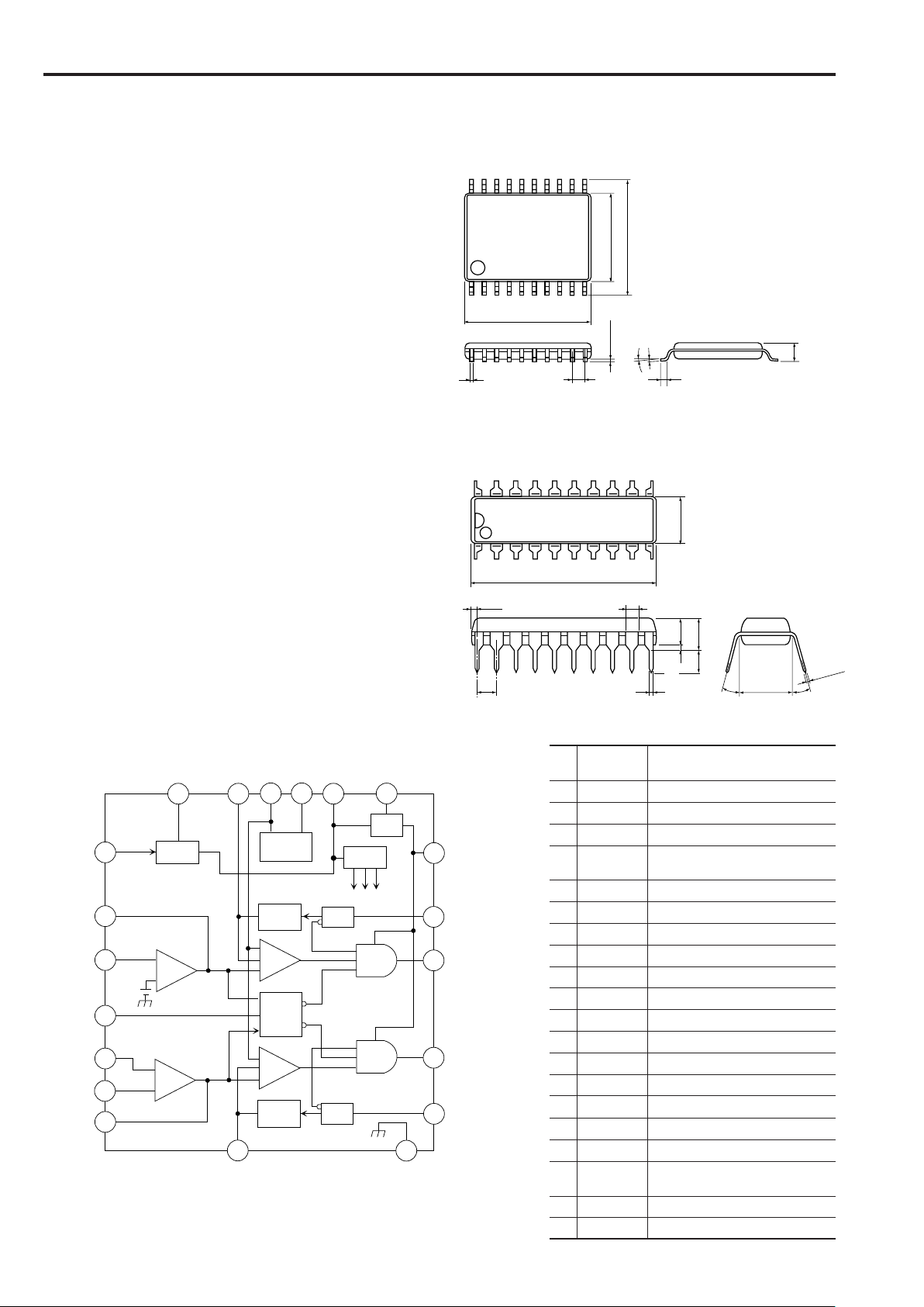
+
-
+
-
+
-
+
-
FB1
ON/OFF
19
17
IN1+
3
CP
IN2+
4
REF
DT1 CT RT VCC1 SW
20
16 1 2 14
13
BIAS
OSC
UVLO
Duty
limit
OCP
12
VCC2
15
OCL1
11
OUT1
PWM1
ER, AMP1
VB
ER, AMP2
PWM2
Duty
limit
OCP
10
OUT2
OCL2
8
GND
DT2
7
6
5
IN2-
FB2
-
Timer
&
latch
18
9
SW
Pin Pin Description
No. symbol
1 CT Oscillator timing capacitor
2 RT Oscillator timing resistor
3 CP Timer and latch circuit
4 IN2+ Non-inverting input to error
amplifier
5 IN2- Inverting input to error amplifier
6 FB2 Error amplifier output
7 DT2 Dead time adjustment
8 OCL2 Overcurrent limiting circuit 2
9 GND Ground
10 OUT2 CH.2 output
11 OUT1 CH.1 output
12 VCC2 Power supply 2
13 SW Switch for boost circuit
14 VCC1 Power supply 1
15 OCL1 Overcurrent limiting circuit 1
16 DT1 Dead time adjustment
17 FB1 Error amplifier output
18 IN1+ Non-inverting input to error
amplifier
19 ON/OFF Output ON/OFF control
20 REF Reference voltage output
■ Block diagram
Page 2

FA7622CP(E)
2
■ Electrical characteristics (Ta = 25°C, VCC = 6V, RT = 36kΩ, CT = 180pF)
Reference voltage section
Item Symbol Test condition Min. Typ. Max. Unit
Output voltage VREF IOR = 1mA 2.400 2.475 2.550 V
Line regulation LINE
V
CC
= 3.6 to 26V, IOR = 1mA
515mV
Load regulation LOAD IOR = 0.1 to 1mA 2 mV
Output voltage variation due to temperature change VTC1 Ta = –30 to +25°C–1 1%
VTC2 Ta = +25 to +85°C–1 1%
Oscillator section
Item Symbol Test condition Min. Typ. Max. Unit
Oscillation frequency fOSC CT = 180pF, RT = 36kΩ 100 110 120 kHz
Frequency variation 1 (due to supply voltage change) fdV VCC = 3.6 to 26V 1 %
Frequency variation 2 (due to temperature change) fdT Ta = –30 to +25°C5%
Error amplifier section (ch. 1)
Item Symbol Test condition Min. Typ. Max. Unit
Reference voltage VB 0.832 0.858 0.884 V
Input bias current IB 5 100 nA
Open-loop voltage gain AVO 40 dB
Unity-gain bandwidth fT 1.0 MHz
Maximum output voltage VOH No load 1.8 V
VOL No load 300 mV
Output source current IOH VOH = 0V 30 60 90
µ
A
Error amplifier section (ch. 2)
Item Symbol Test condition Min. Typ. Max. Unit
Input offset voltage VIO 210mV
Input bias current IB 5 100 nA
Common-mode input voltage VCOM 0 1.0 V
Open-loop voltage gain AVO 70 dB
Unity-gain bandwidth fT 1.0 MHz
Maximum output voltage VOH No load 1.8 V
VOL No load 300 mV
Output source current IOH VOH = 0V 40 80 120
µ
A
■ Absolute maximum ratings
Item Symbol Rating Unit
Supply VCC1 28 V
voltage
VCC1 20 V
Supply voltage VCC2 28 V
ON/OFF pin voltage VON/OFF –0.3 to +7 V
Out pin output current IOUT ±600 mA
Total power dissipation Pd 650 mW
Junction temperature Tj 125 °C
Operating temperature Topr –30 to +85 °C
Storage temperature Tstg –40 to +150 °C
Voltage boost
circuit not used
Voltage boost
circuit used
■ Recommended operating conditions
Item Symbol Min. Max. Unit
VCC1 3.6 26 V
VCC1 3.6 18 V
RNF 100 kΩ
CT 50 2200 pF
RT 24 100 kΩ
fOSC 50 1000 kHz
Supply
voltage
Feedback resistance
Timing capacitance
Timing resistance
Oscillation frequency
Voltage boost
circuit not used
Voltage boost
circuit used
Page 3

FA7622CP(E)
3
Pulse width modulation circuit section ( FB1, FB2 pin )
Item Symbol Test condition Min. Typ. Max. Unit
Input threshold voltage VTHO Duty cycle = 0% 1.6 1.8 V
Input threshold voltage VTHI Duty cycle = 100% 0.8 1.0 V
Dead time adjustment circuit section ( DT1, DT2 pin )
Item Symbol Test condition Min. Typ. Max. Unit
Input threshold voltage VTH0 Duty cycle = 0% 1.6 1.8 V
Input threshold voltage VTH1 Duty cycle = 100% 0.8 1.0 V
Standby voltage VSTR DT1, DT2 pin open 1.8 V
Overcurrent limiting circuit section
Item Symbol Test condition Min. Typ. Max. Unit
Input threshold voltage VTHOC 180 210 240 mV
Hysteresis voltage VHYOC 40 mV
Input bias current IOC 50 100
µ
A
Delay in OCL tdoc Overdriving: 50mV 120 ns
Timer and latch circuit section
Item Symbol Test condition Min. Typ. Max. Unit
Latch-mode threshold voltage VTHCP 1.00 1.25 1.50 V
Input bias current IINCP VCP = 1.5V, VFB = 0.3V 1
µ
A
CP pin voltage / LOW VSATC ICP = 20 µA, VFB = 1.0V 300 mV
Output ON/OFF control circuit section
Item Symbol Test condition Min. Typ. Max. Unit
OFF-to-ON threshold voltage VTHON 3.0 V
ON-to-OFF threshold voltage VTH OFF 0.60 V
Input bias current IIN VIN = 3V 180
µ
A
Undervoltage lock-out circuit section
Item Symbol Test condition Min. Typ. Max. Unit
OFF-to-ON threshold voltage VCCON 2.80 3.00 3.20 V
ON-to-OFF threshold voltage VCCOF 2.90 V
Voltage hysteresis VHYS 0.10 V
Output section
Item Symbol Test condition Min. Typ. Max. Unit
Saturation voltage (H level) VSAT+ IO = –50mA 1.50 2.00 V
Saturation voltage (L level) VSAT–
I
O
= 50mA
1.70 2.20 V
Voltage step-up circuit section
Item Symbol Test condition Min. Typ. Max. Unit
Output voltage VOUP L=330µH, C=1µF, No load 10.5 12.5 14.0 V
Overall device
Item Symbol Test condition Min. Typ. Max. Unit
Stand-by supply current ICCST Out pin open 0.1 10
µ
A
Operating VCC1 current ICC1 Normal operation 3.8 5.5 mA
Operating VCC2 current ICC2 Normal operation VCC2=12V 1.5 2.2 mA
OUT1, OUT2 open
Duty cycle=50%
Page 4

FA7622CP(E)
4
1. Oscillator section
This section charges and discharges an external capacitor C
T.
The charge current is determined by the external resistor R
T
connected to the IC. By charging and discharging the
capacitor, this section provides a 1.0 to 1.6V triangle wave at
the CT pin. The oscillation frequency can be set between
50kHz to 1MHz. The frequency can be
calculated approximately as follows:
f
OSC ( kHz ) ⫽
7.1 • 10
5
RT ( kΩ ) • CT ( pF )
(1)
...................…
2. Error amplifier section
Error amplifier
➀
As Fig. 3 shows, the inverting input of the error amplifier is
connected to the V
B reference voltage (0.858V typ.). The non-
inverting input IN1+ and output FB1 connect to external
terminals.
During ordinary operation, the IN1+ terminal voltage is almost
equal to V
B. The power-supply output VOUTA can be
determined as follows:
V
OUTA ⫽
R1 + R2
R2
(2)
.................................…
•V
B
The DC gain of the error amplifier is 40dB (typ.), regardless of
external parts connected to the IC. Correct the phase by
connecting capacitor C
1 between the VOUTA and FB1 pins.
Error amplifier
➁
• Voltage step-up or step-down chopper circuit
As Fig. 4 shows, the non-inverting input IN2+, inverting input
IN2–, and output FB2 of the error amplifier are connected to
external terminals.
The feedback voltage V
OUTB to the IN2+ pin can be
determined as follows:
V
OUTB ⫽
( R3 + R4 ) • R6
R4 • ( R5 + R6 )
(3)
..................……
• V
REF
The DC gain AV from the VOUTB to FB2 pin is 70dB (min),
when R
7 is not connected.
When R
7 is connected, the AV can be determined as follows:
AV ⫽
R
4
R3 + R4
(4)
...........
• 1 +
R
7 • (R5 + R6)
R
5 • R6
Fig. 3
To correct the phase, connect the resistor R8 and capacitor C2
in series between the IN2– and FB2 pins.
Fig. 4
Fig. 1 Oscillator
1
2
RTCT
C
T
V =1.0 (V)
RT
I = 앐
CT
1.0 (V)
R
T
R
T
1.0V
1.6V
CT pin voltage waveform
O S C
1
REF
CT
C
T
20
9
GND
I
V : 1.0
→ 1.6V
CT
CT
I
V : 1.6
→ 1.0V
CT
CT
Fig. 2
10
20
⫹
⫺
6
R3
VOUTB
FB2
ER.AMP2
C2
R4
R6
R5
IN2
IN2
REF
Q2
R8
R7
5
4
+
-
(Controlled by Q2)
OUT2
R1
18
17
11
⫹
⫺
VOUTA
R2
FB1
IN1
ER.AMP1
Q1
C1
+
(Controlled by Q1)
V
B
36kΩ
OUT1
■ Description of each circuit
Page 5

FA7622CP(E)
5
• Inverting chopper circuit
According to the circuit shown in Fig. 5, the power output
voltage V
OUTB can be determined as follows:
V
OUTB = –
R
11
R10
(5)
..............................
• V
REF
The AV between the VOUTB and FB2 pins can be determined
as follows:
A
V ⫹
–R11
R12
(6)
.................................................
To correct the phase, connect the resistor R
13 and capacitor
C
3 in series between the IN2– and FB2 pins.
By using this circuit, invert the output polarity of OUT2 with an
external transistor to drive a P-channel MOSFET (or PNP
transistor).
3. PWM comparator section
As Fig. 6 shows, a PWM comparator has three input
terminals. PWM comparator 1 determines the duty cycle of
the output from the OUT1 pin. This comparator compares the
C
T oscillator Voltage (Pin 1) with the FB1 voltage (Pin 17) or
the DT1 voltage (Pin 16), whichever is greater. When the
highest of these voltages is lower than the C
T voltage, the
PWM output is high. When it is higher than C
T, the PWM
output is low.
PWM comparator 2 determines the duty cycle of the output
from the OUT2 pin. To determine the PWM output, this
comparator compares the C
T oscillator voltage (Pin 1) with the
FB2 voltage (Pin 6) or the DT2 voltage (Pin 7) whichever is
higher.
During ordinary operation, the OUT1 and OUT2 pin voltages
have the same polarity as the output from each comparator.
When the power supply is turned on, the pulse width
gradually increases. The time constant for soft-start is
determined by the external resistor and capacitor across pins
16 and 7. In Figures 7 and 8, the time ts required for the pulse
width (duty-cycle) to reach about 30% after start-up can be
determined as follows:
(Units: µF for Cs and kΩ for Rs, Rs1, and Rs2)
Fig. 5
Fig. 8
Fig. 6
⫹
⫺
C3
Q3
FB2
R10
R9
REF
R11
R12
R13
IN2
IN2
ER.AMP2
V
CC1
+
-
VOUTB(Controlled by Q3
)
10
20
6
5
4
OUT2
⫹
⫺
PWM output
FB1(FB2)
DT1(DT2)
Time
CT
PWM output
PWM1
(PWM2)
DT1(DT2)
FB1(FB2)
CT
⫺
Fig. 7
DT1(DT2)
20
⫹
⫺
1
FB1(FB2)
CS
CT
RS
REF
PWM output
PWM1
(PWM2)
⫺
20
⫹
⫺
1
⫺
DT1(DT2)
FB1(FB2)
C
S
CT
R
S2
REF
PWM output
PWM1
(PWM2)
R
S1
Fig.8:
t
S (mS) = CS • ln
R
S1
0.417RS1 – 0.583 RS2
(7)
.................................
Fig.7:
t
S (mS) = 0.54CS • RS
Where, RS1 / RS2 > 0.716
(8)
……
R
S1 • RS2
RS1 ⫹ RS2
Please connect enough large capacitance between REF and
GND pins in order to prevent irregular output pulse caused by
minus voltage at DT1 or DT2 pin when IC is shut down.
Page 6

FA7622CP(E)
6
4. Timer and latch circuit for overload protection
Figure 9 shows the timer and latch circuit for overload
protection and Fig. 10 shows its timing during an overload.
If the power supply output decreases due to an overload, the
error amplifier output decreases. If the voltage decreases to
less than 0.3V, the switch that clamps the CP pin voltage to
the ground disconnects. This charges capacitor Cp from the
REF pin through the resistor Rcp and the CP pin voltage
increases. When the voltage reaches 1.25V, OUT1 (OUT2)
voltage is clamped to ground.
The N-channel MOSFET (or NPN transistor) connected to the
OUT1 (or OUT2) is turned OFF and cuts off the power supply.
The time t
L from when the circuit is overloaded until the power
supply is cut off can be determined as follows:
(9)
.................
t
L (mS) = 0.67CP (µF) • RCP (kΩ)
5. Overcurrent limiting circuit
This is a pulse-by-pulse overcurrent limiting circuit which
detects and limits the peak of each drain current pulse from the
main switching transistor (MOSFET).
Figure 11 shows the overcurrent limiting circuit and Fig. 12
shows its timing.
This circuit detects a drain current with a voltage sampling
resistor Rs. If a voltage lower than the VCC1 pin voltage by
210mV or more is input to OCL1 (OCL2), the OUT1 (OUT2) is
clamped to ground. At the same time, DT1 (DT2) is raised to
the reference voltage V
REF. (This reduces the duty-cycle to
0%)
This circuit has hysteresis to prevent noise from causing
malfunction.
The R
S voltage which is propotional to drain current is limited
to 210mV (typ.) and released at 170mV (typ).
Fig. 9
Fig. 10
Fig. 11
Fig. 12
⫺
OUT1
(OUT2)
OCL1
(OCL2)
VCC1
-0.21V
REF
DT1
(DT2) VCC1
D
I
⫹
Rs
OUT1
(OUT2)
Time
VCC1
VCC1
-0.2V
OCL1
(OCL2)
(Similar to ID)
Voltage waveforms
PWM output
FB1(FB2)
DT1(DT2)
Time
CP
CT
1.25V
(Threshold voltage
of CP pin)
Voltage waveforms
20
⫹
⫺
⫹
⫺
1.25V
CP
S1
REF
OUT1
(OUT2)
RCP
FB1
(FB2)
0.3V
CP
Page 7

FA7622CP(E)
7
6. IC ON/OFF control circuit
This control circuit turns the entire IC ON or OFF by an
external signal using an ON/OFF control pin to limit the IC’s
current consumption to 10µA or less.
Figure 13 shows the IC ON/OFF control circuit and Fig. 14
shows its timing.
To turn the IC OFF, this circuit clamps OUT1 (OUT2) to
ground when the ON/OFF pin voltage is controlled to less than
0.60V. The internal bias current is cut off to turn off the
switching transistor.
To turn the IC ON, raise the ON/OFF pin voltage immediately
to 3.0V or more to charge the soft-start capacitor gradually.
7. Voltage boost circuit
By using the circuit shown in Fig. 15, this IC generates a
voltage 6.5V (typ.) higher than the VCC1 input voltage at the
VCC2 pin. This circuit allows the IC to drive MOSFET gates
directly. With this circuit, the IC can drive a low-level side
N-channel MOSFET at 3.6 to 18V as VCC1 (not possible with
conventional ICs). In addition, an N-channel MOSFET can be
used on the high-level side of a buck chopper. In Fig. 15, the
inductor (L) is about 100µH or more and the capacitor (Cup)
should be greater than about 0.1µF.
If voltage boost is not necessary, connect the VCC1 and VCC2
pins directly, and SW pin must be opened.
8. Undervoltage lock-out circuit
This circuit prevents a malfunction at a low supply voltage.
When the supply voltage VCC1 rises and reaches 3.0V, this
circuit is activated. When VCC1 drops below 2.9V, this circuit
clamps OUT1 (OUT2) to ground. The CP pin voltage is reset
to low by means of cutting off a power supply input.
9. Output circuit
As Fig. 17 shows, OUT1 and OUT2 with a totempole
structure can drive a MOSFET.
Since both the maximum output source and sink currents are
600mA, a MOSFET can be switched at high speed.
Fig. 14 Control of output
Fig. 16
ON/OFF
3.0V
⫹
⫺
0.6V
OUT1
(OUT2)
ID
Fig. 13
OUT1
(OUT2)
Time
0V
ON/OFF
3.0V
Voltage waveforms
14 13 12
VCC1 VCC2SW
LD
CUP
R E G U L A T O R
Fig. 15
GND
OUT1
(OUT2)
VCC2
Page 8

FA7622CP(E)
8
■ Application circuit
Parts tolerances characteristics are not defined in the circuit design
sample shown above. When designing an actual circuit for a product,
you must determine parts tolerances and characteristics for safe and
economical operation.
+
+
+
+
20
19
18
17
16 15
14
13 12 11
10987
6
5432
1
REF
ON/OFF
IN1+ FB1
DT1
OCL1
VCC1 SW
OUT1
VCC2
OUT2GNDOCL2
DT2FB2
IN2-
IN2+CP
RTCT
FA7622P(M)
2.2k
10.6k
470k
683
683
684
330
472
330µ
683
1µ
10
0.33
47k
100µ
33µ
VIN
5.5~9V
5V
47µ
12V
100µ
33µ
0.33
47k
10
330
472
120k
470k
3.3k
102
360k
510k
683
180p
3.3K
100k
ON/OFF
1µ
64k
36k
 Loading...