

Page 1
FA7615CP(E)
1
■ Description
The FA7615CP(E) is a bipolar IC containing basic circuit
necessary for PWM-type switching power supply control. This
IC can be operated by external synchronizing pulses.
■ Features
• External synchronization input terminal
• Low-voltage operation (V
CC = 3.6 to 22V)
• Totem-pole predriver
• Latch-mode short-circuit protection function (no malfunction
due to electrical noise)
• One capacitor shared for short-circuit protection and for softstart to minimize the number of external discrete components
■ Applications
• Battery power supply for portable equipment
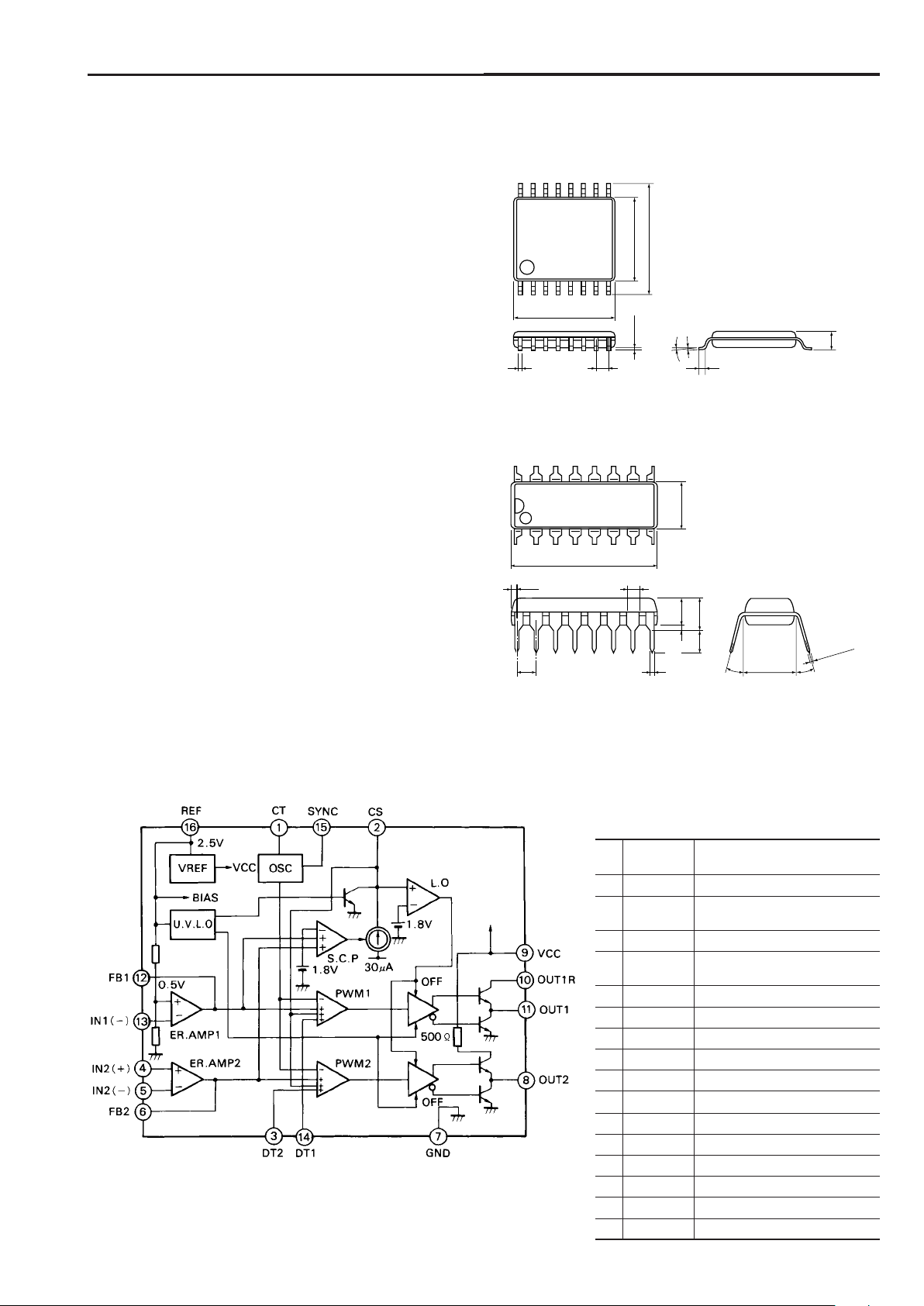
■ Dimensions, mm
Á SSOP-16
1
8
9
16
0.6
0~10˚
0.65
7.9
±0.3
5.3
6.2
0.1
±0.1
0.2
+0.1
–0.05
0.3
2.1max
Á DIP-16
■ Block diagram
FA7615CP(E)
Bipolar IC
For Switching Power Supply Control
Pin Pin Description
No. symbol
1 CT Oscillator timing capacitor
2 CS
Capacitor for soft-start,
short-circuit protection and delay
3 DT2 Dead time adjustment
4 IN2 (+) Non-inverting input to error
amplifier
5 IN2 (–) Inverting input to error amplifier
6 FB2 Error amplifier output
7 GND Ground
8 OUT2 CH. 2 Output
9 VCC Power supply
10 OUT1R CH. 1 Current limiting resistor
11 OUT1 CH. 1 Output
12 FB1 Error amplifier output
13 IN1 (–) Inverting input to error amplifier
14 DT1 Dead time adjustment
15 SYNC External synchronization input
16 REF Reference voltage output (2.5V)
1
16
9
8
19.4
6.5
7.6
3.4
4.3max
1.5
0.81
3.1min
0.2min
0~15˚
0~15˚
0.5
±0.1
2.54
±0.25
0.3
+0.1
–0.05
Page 2
FA7615CP(E)
2
■ Electrical characteristics (Ta = 25°C, VCC = 6V, RT = 47kΩ, CT = 1000pF)
Reference voltage section
Item Symbol Test condition Min. Typ. Max. Unit
Output voltage VREF IOR = 1mA 2.383 2.432 2.481 V
Line regulation LINE VCC = 3.6 to 20V, IOR = 1mA 4 12 mV
Load regulation LOAD IOR = 0.1 to 1mA 1 6 mV
Output voltage variation due to temperature change VTC1 Ta = –20 to +25°C–1 1%
VTC2 Ta = +25 to +85°C–1 1%
Oscillator section
Item Symbol Test condition Min. Typ. Max. Unit
Oscillation frequency fOSC CT = 1000pF, RT = 47kΩ 17 20 23 kHz
Frequency variation 1 (due to supply voltage change) fdV VCC = 3.6 to 20V 1 %
Frequency variation 2 (due to temperature change) fdT Ta = –20 to +85°C5%
Synchronizing terminal input current ISYNC VSYNC = 2V 0.4 1.0 mA
Synchronizing terminal input voltage VSYNC 1 2.5 V
Error amplifier section
Item Symbol Test condition Min. Typ. Max. Unit
Reference voltage VB 0.484 0.494 0.504 V
Input bias current IB 5 100 nA
Open-loop voltage gain AV 70 dB
Unity-gain bandwidth GB 1.0 MHz
Maximum output voltage (Pin 6 and Pin 12) VOM+ RNF = 100kΩ
V
REF
–0.2
V
VOM– RNF = 100kΩ 200 mV
Output source current (Pin 6 and Pin 12) IOM+ VOM = 1V 40 85 200
µ
A
PWM comparator section
Item Symbol Test condition Min. Typ. Max. Unit
Input threshold voltage (Pin 6 and Pin 12) VTH0 Duty cycle = 0% 0.38 0.48 V
Input threshold voltage (Pin 6 and Pin 12) VTH50 Duty cycle = 50% 0.6 V
■ Absolute maximum ratings
Item Symbol Rating Unit
Supply voltage VCC 22 V
Reference voltage output current
IOR 5mA
Output current IO ±50 mA
Total power dissipation Pd 400 mW
Operating temperature Topr –20 to +85 °C
Storage temperature Tstg –40 to +150 °C
■ Recommended operating conditions
Item Symbol Min. Max. Unit
Supply voltage VCC 3.6 20 V
Feedback resistance RNF 100 kΩ
Oscillator timing capacitor CT 220 22,000 pF
Oscillator timing resistance RT 10 100 kΩ
Oscillation frequency fOSC 5 200 kHz
Page 3

FA7615CP(E)
3
Dead time adjustment circuit section
Item Symbol Test condition Min. Typ. Max. Unit
Input bias current (Pin 3 and Pin 14) IBDT 80 300 nA
Input threshold voltage (Pin 3 and Pin 14) VTH DT0 Duty cycle = 0% 0.38 0.48 V
Input threshold voltage (Pin 3 and Pin 14) VTH DT50 Duty cycle = 50% 0.60 V
Short-circuit protection circuit section
Item Symbol Test condition Min. Typ. Max. Unit
Input threshold voltage (Pin 6 and Pin 12) VTH PC 1.60 1.80 2.00 V
Charge current (Pin 2) ICHG
Pin 2 = 0V, Pin 6, Pin 12 = 2V
18 30 42
µ
A
Latch-mode threshold voltage (Pin 2) VTH LA 1.60 1.80 2.00 V
Undervoltage lockout section
Item Symbol Test condition Min. Typ. Max. Unit
OFF-to-ON threshold voltage VTH ON 2.65 V
ON-to-OFF threshold voltage VTH OFF 2.60 V
Voltage hysteresis VHYS 50 mV
Output section
Item Symbol Test condition Min. Typ. Max. Unit
Output saturation voltage H-level (CH.1) VO1H
Output source current = 20mA
0.3 0.8 V
L-level (Common to CH.1 and CH.2)
VO1L/2L Output sink current = 20mA 0.3 0.8 V
CH. 1 Output source current (Pin 11) ISOURCE1 Pin 11 = 0V 6 11 15 mA
CH. 2 Output source current (Pin 8) ISOURCE2 VCC = 16V, Pin 8 = 0V 19 27 36 mA
Overall device
Item Symbol Test condition Min. Typ. Max. Unit
Supply current ICC LA Latch mode 2.0 3.0 mA
Operating-state supply current ICC AV RL = ∞ Duty cycle = 50% 3.5 6.0 mA
Page 4

FA7615CP(E)
4
■ Characteristic curves (Ta = 25°C)
Oscillation frequency (fOSC) vs. Output duty cycle vs. CS terminal voltage (VCS)
timing resistor resistance (R
T)
Output duty cycle vs. DT terminal voltage (VDT) Output duty cycle vs. FB terminal voltage (VFB)
H-level output saturation voltage (VO1H) CH-2 output source current (ISOURCE2)
vs. CH. 1 output source current (I
SOURCE1) vs. supply voltage (VCC)
VO1H [V]
ISOURCE [mA]
Page 5

FA7615CP(E)
5
L-level output voltage (VOL) vs. output sink current (ISINK) Supply current (ICC) vs. supply voltage (VCC)
Error amplifier frequency (f) vs. voltage gain (AV)/phase (θ)
AV[dB]
f [Hz]
Phase θ [deg]
Page 6

FA7615CP(E)
6
■ Application circuit
Á Flyback-transformer type and chopper type boost converter circuit
Parts tolerances characteristics are not defined in the circuit design
sample shown above. When designing an actual circuit for a product,
you must determine parts tolerances and characteristics for safe and
economical operation.
Please connect a capacitor, which the value is about 0.01µF to 0.1µF,
between VCC and REF terminals in order to prevent from irregular
output pulse at start-up.
 Loading...