

Page 1

FA5500AP/AN, FA5501AP/AN
Quality is our message
Quality is our message
Quality is our messageQuality is our message
FUJI Power Supply Control IC
Power Factor Correction
FA5500AP/AN
FA5501AP/AN
1
November `02
Fuji Electric Co., Ltd.
Matsumoto Factory
Page 2

FA5500AP/AN, FA5501AP/AN
1.This Data Book contains the product specifications, characteristics, data, materials, and structures
as of November 2002. The contents are subject to change without notice for specification changes
or other reasons. When using a product listed in this Data Book, be sure to obtain the latest
specifications.
2. All applications described in this Data Book exemplify the use of Fuji's products for your reference
only. No right or license, either express or implied, under any patent, copyright, trade secret or other
intellectual property right owned by Fuji Electric Co., Ltd. is (or shall be deemed) granted. Fuji
makes no representation or warranty, whether express or implied, relating to the infringement or
alleged infringement of other's intellectual property rights which may arise from the use of the
applications descri bed herein.
3. Although Fuji Electric is enhancing product quality and reliability, a small percentage of
semiconductor products may become faulty. When using Fuji Electric semiconductor products in
your equipment, you are requested to take adequate safety measures to prevent the equipment
from causing a physical injury, fire, or other problem if any of the products become faulty. It is
recommended to make your design fail-safe, f la m e ret ardant , and free of malfunction.
4.The products introduced in this Data Book are intended for use in the following electronic and
electrical equipment w h i ch has normal reliability requirements.
• Computers • OA equipment • Communications equip me nt (t erminal devices)
• Measurement equipment • Machine tools • Audiovisual equipment • Electrical home
appliances • Personal equipment • Industrial robots etc.
5.If you need to use a product in this Data Book for equipment requiring higher reliability than normal,
such as for the equipment listed below, it is imperative to contact Fuji Electric to obtain prior
approval. When using these products for such equipment, take adequate measures such as a
backup system to prevent the equipment from malfunctioning even if a Fuji's product incorporated in
the equipment becomes f ault y.
• Transportation equipment (mounted on cars and ships) • Trunk communications equipment
• Traffic-signal control equipment • Gas leakage detectors with an auto-shut-off feature
• Emergency equipment for respondi ng t o disasters and anti-burglary dev ices • Safety devices
6. Do not use products in this Data Book for the equipment requiring strict reliability such as (without
limitation)
• Space equipment • Aeronautic equipment • Atomic control equipment
• Submarine repeater equipment • Medical equipment
7. Copyright © 1995 by Fuji Electric Co., Ltd. All rights reserved. No part of this Data Book may be
reproduced in any form or by any means without the express permission of Fuji Electric.
8. If you have any question about any portion in this Data Book, ask Fuji Electric or its sales agents
before using the product. Neither Fuji nor its agents shall be liable for any injury caused by any use
of the products not in accordance with i nst ruct i ons set forth herein.
WARNING
Quality is our message
Quality is our message
Quality is our messageQuality is our message
2
Page 3

FA5500AP/AN, FA5501AP/AN
Quality is our message
Quality is our message
Quality is our messageQuality is our message
CONTENTS
1. Description ……………. 4
2. Features ……………. 4
3. Outline ……………. 4
4. Types of FA5500A/01A ……………. 4
5. Block diagram ……………. 5
6. Pin assignment ……………. 5
7. Ratings and c h aracteristics ……………. 6 – 8
8. Characteristic c ur ves ……………. 9 – 12
Pages
9. Description of PFC converter ……………. 13 – 14
10. Description of e ac h circuit ……………. 15 – 18
11. Design advice ……………. 19 –25
12. Example of a p pl ic ation circuit ……………. 26
Note
• Parts tolerance and characteristics are not defined in all application described in this Data book. When design an
actual circuit for a product, you must determine parts tolerances and characteristics for safe and economical
operation.
3
Page 4
FA5500AP/AN, FA5501AP/AN
Quality is our message
Quality is our message
Quality is our messageQuality is our message
1. Description
FA5500A/FA5501A are control ICs for a power factor correction converter using critical conduction mode of operation.
This IC uses a CMOS device with high dielectric strength (30V) to implement low power consumption. These ICs contain
compensated current sense comparator for light load and open/short protection at feedback (FB) pin. Compensated current
sense comparator for light load keeps output voltage constant from no-load to full-load. Open/short protection at FB pin
stops output pulses when voltage divider to detect output voltage becomes fault.
2. Features
• Low current consumption by CMOS process
Start-up : 20µA(max.), Operating : 1mA(typ.)
• Drive circuit for connecting a power MOSFET directly
• Output peak current, source : 500mA, sink : 1000mA
• Compensated current sense compar ator for light load
• Open/short protection at feedback (FB) pin
• Undervoltage Lockout
FA5500A: 11.5V ON / 9V OFF FA5501A:13V ON / 9V OFF
• Overvoltage protection
• Restart timer
• Package: DIP-8 / SOP-8
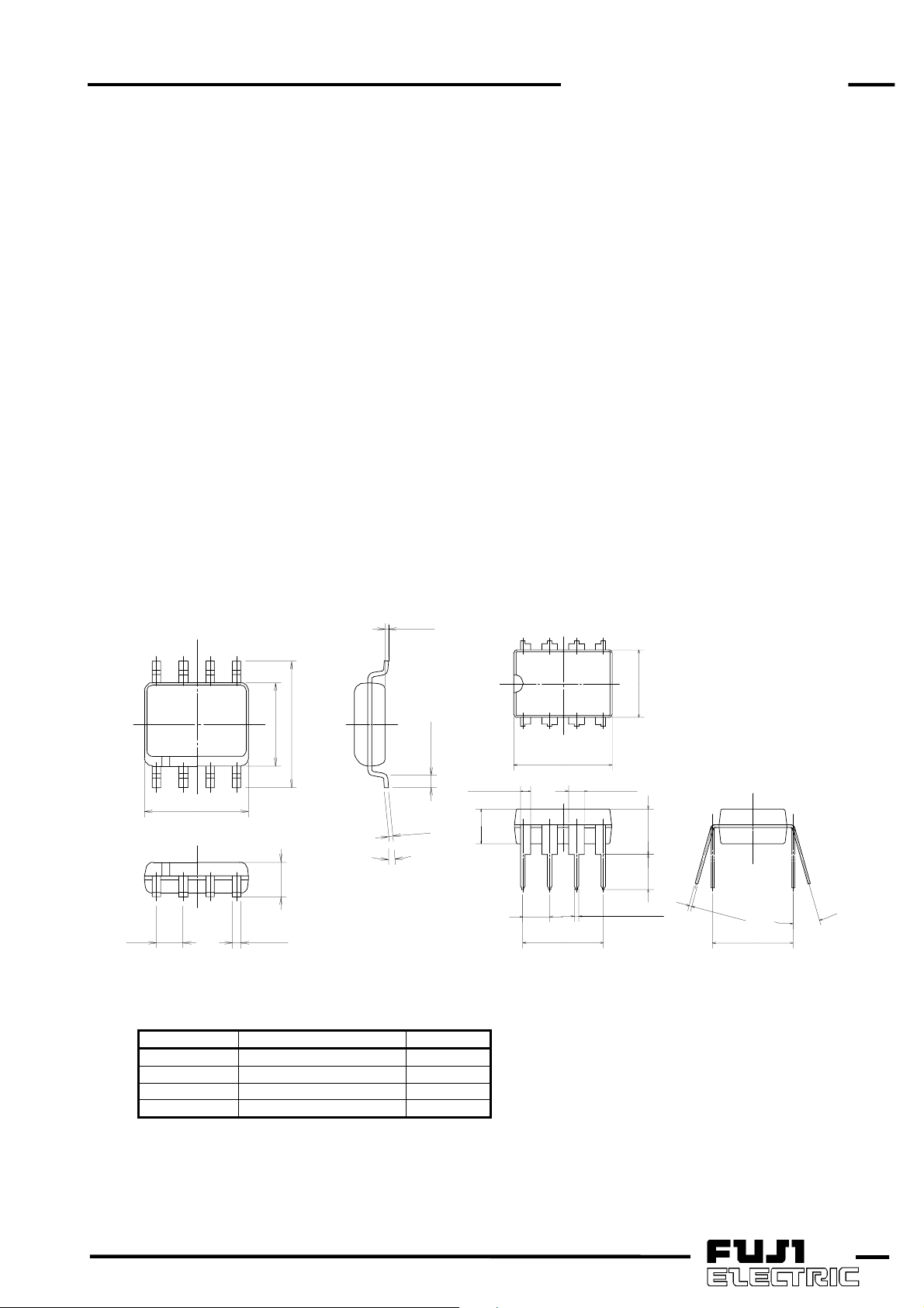
3. Outline
SOP-8 DIP-8
5
4
0.4 ±0.1
3.9
6 ±0.2
8
1
4.9
1.27
4. Types of FA5500A/01A
Type Startup Threshold Package
FA5500AP 11.5V(typ.) DIP-8
FA5500AN 11.5V(typ.) SOP-8
FA5501AP 13V(typ.) DIP-8
FA5501AN 13V(typ.) SOP-8
1.8 MAX
0.18 ±0.08
0.65 ±0.25
+0.10
0.20
-0.05
oo
80 −
1.0 ±0.3
3.3
8
1
2.54
2.54×3=7.62
9.3
5
4
1.5 ±0.3
0.46 ±0.1
6.4
3 MIN 4.5 MAX
0.25
+0.1
- 0.05
7.62
oo
150 −
4
Page 5
FA5500AP/AN, FA5501AP/AN
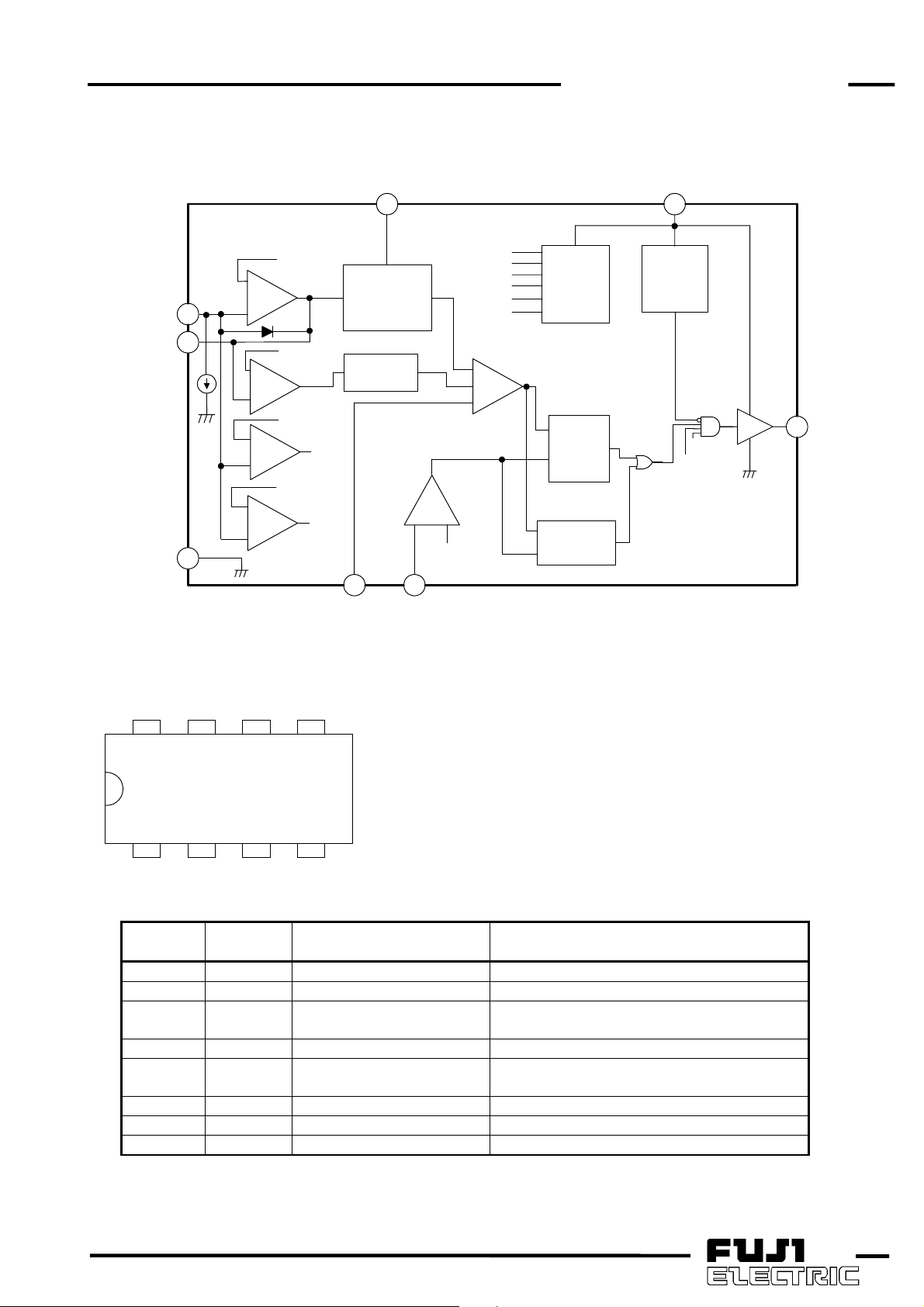
5. Block diagram
Quality is our message
Quality is our message
Quality is our messageQuality is our message
FB
COMP
2.5µA
GND
MUL
VREF(2.5V)
+
1
2
6
ERRAMP
-
+
-
-
+
+
-
VOS(2.0V)
VSP(0.3V)
SP
VOVP
(1.09VREF)
OVP
MUL
AOC
VREF(2.5V)
VDD(5.0V)
VOVP(1.09VREF)
VZCD(1.5V/1.33V)
VOS(2.0V)
VSP(0.3V)
+
-
+
-
VZCD(1.5V/1.33V)
54
REF
R
S
R
TIMER
R
Q
VCC
83
UVLO
SP
OVP
7
OUT
ZCDIS
6. Pin assignment
OUTVCC GND ZCD
8765
1234
FB COMP MUL IS
Pin No. Pin
symbol
1 FB Voltage Feedback Input Input for monitoring PFC output voltage
2 COMP Compensation Output of error amplifier
3 MUL Multiplier Input Input of multiplier for monitoring sinusoidal
4 IS Current Sense Input Input for sensing MOSFET current signal
5 ZCD Zero Current Detect Input Input for detecting that the inductor current
6 GND Ground Ground
7 OUT Output Output for direct driving a power MOSFET
8 VCC Power Supply Power supply for IC
Function Description
waveform
reaches zero
5
Page 6
FA5500AP/AN, FA5501AP/AN
Quality is our message
Quality is our message
Quality is our messageQuality is our message
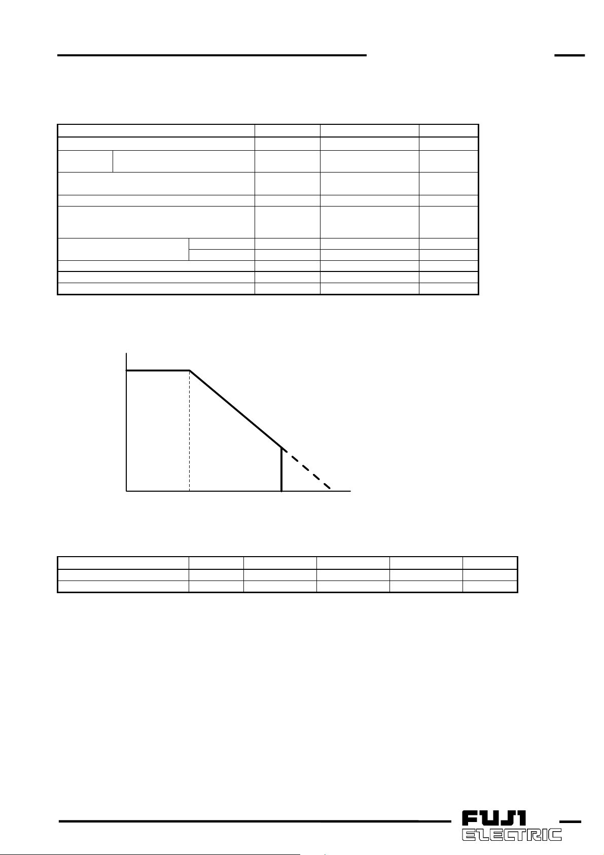
7. Ratings and characteristics
The contents are subject to change without notice. When using a product, be sure to obtain the latest specifications.
(1) Absolute Maximum Ratings
Item Symbol
Total Power Supply and Zener Current Icc+Iz 30 mA
Supply
Voltage
Output Current Sink
Source
Input voltage(IS,MUL,FB) Vin -0.3 to 5 V
Zero Current Detect Input
High State Forward Current
Low State Reverse Current
Operating Ambient Temperature Ta -30 to +105 °C
Operating Junction Temperature Tj +150 °C
Storage Temperature Tstg -55 to +150 °C
Maximum dissipation curve
400mW(SOP)
800mW(DIP)
Zener Clamp (Icc+Iz<30mA) Vcc Self Limiting V
Io
Iin
DIP-8 Pd1 800 mW Power dissipation
SOP-8 Pd2 400 mW
Ratings Unit
+1000
-500
-50
10
mA
mA
mA
Maximum dissipation Pd [mW]
-30 25 105 150
Ambience temperature Ta(°C)
(2) Recommended Operating Conditions
Item Symbol Min Typ Max Unit
Supply Voltage Vcc 10 12 28 V
ZCD pin current Izcd ±3 mA
6
Page 7
FA5500AP/AN, FA5501AP/AN
Quality is our message
Quality is our message
Quality is our messageQuality is our message
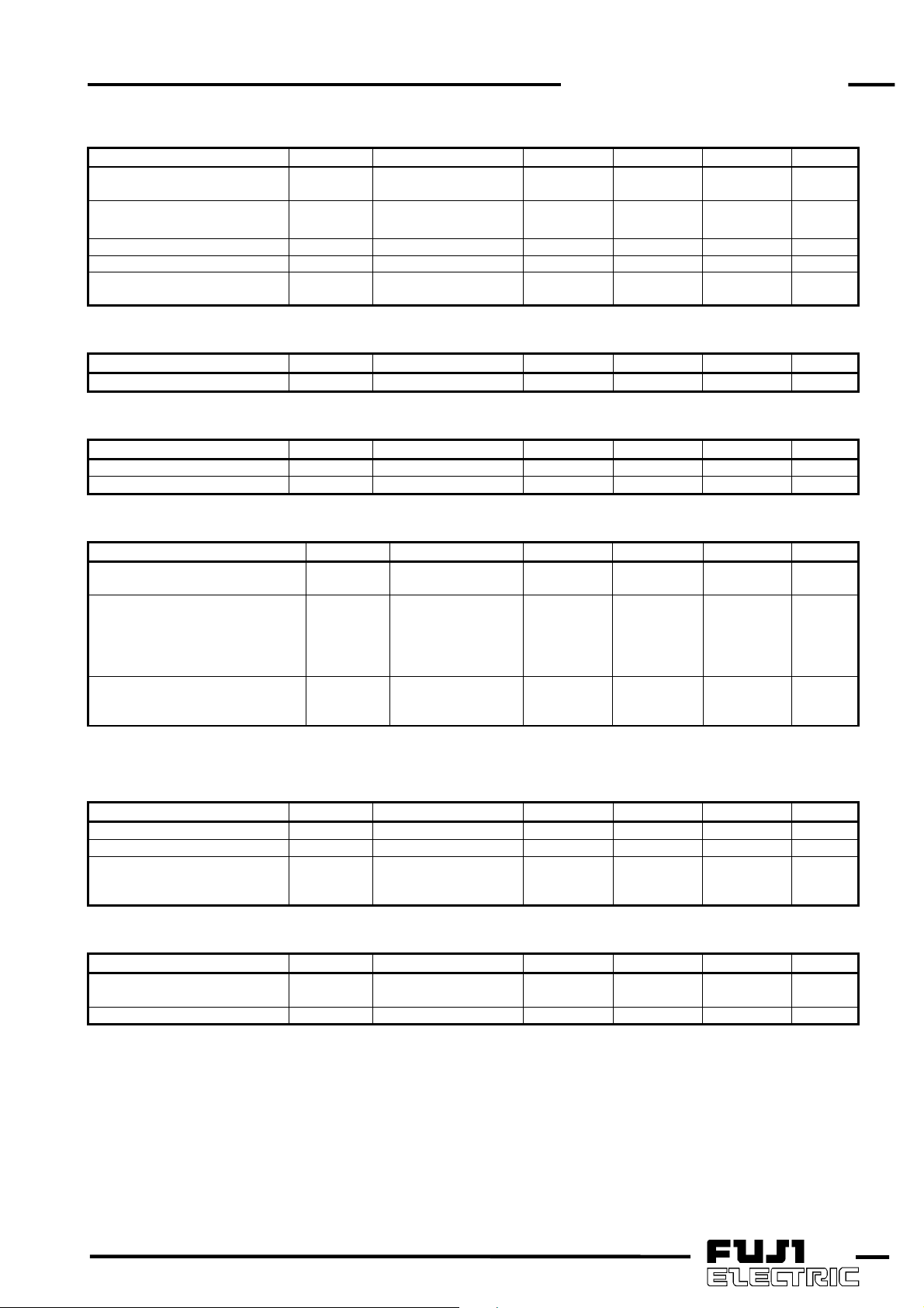
(3) Electrical Characteristics (Unless otherwise specified, Ta=25°C and Vcc=12V)
ERROR AMPLIFIER(FB,COMP Pin)
Item Symbol Condition Min Typ Max Unit
Voltage Feedback Input
Threshold
Line Regulation Regline
Temperature stability VdT Ta=-30°C to +105°C ±0.5 mV/°C
Transconductance Gm Ta=25°C 70 90 120 µmho
Output Current Io
OVERVOLTAGE COMPARATER (FB Pin)
Item Symbol Condition Min Typ Max Unit
Input Threshold Vthovp 1.075Vfb 1.09Vfb 1.105Vfb V
FB SHORT COMPARATOR(FB Pin)
Item Symbol Condition Min Typ Max Unit
Input Threshold Vthsht 0.1 0.3 0.5 V
Pulldown Current Ifb 0.5 2.5 5 µA
MULTIPLIER(COMP,MUL Pin)
Item Symbol Condition Min Typ Max Unit
Input Threshold
Pin2(COMP)
Dynamic Input Voltage Range
Pin3(MUL)
Pin2(COMP)
Gain K
K=Pin4Threshold/{Vpin3(Vpin2-Vthcomp)}
Vfb Ta=25°C 2.465 2.500 2.535 V
Vcc=12V to 28V
Ta=25°C
Source(Vfb=2.3V)
Sink(Vfb=2.7V)
Vthcomp 1.79 2.04 - V
Vpin3
Vpin2
Vpin3=0.5V
Vpin2=Vthcomp
+1.0V
-50 -20 - mV
-
-
0 to 2.5
Vthcomp to
Vthcomp
+1.0
0.53 0.75 0.97 1/V
10
10
0 to 3.5
Vthcomp to
Vthcomp
+1.5
-
-
-
µA
V
ZERO CURRENT DETECTOR (ZCD Pin)
Item Symbol Condition Min Typ Max Unit
Input Threshold Voltage Vthzcd Vin increasing 1.33 1.50 1.87 V
Hysteresis Vh Vin decreasing 100 170 300 mV
Input Clamp Voltage
“H” state
“L” state
CURRENT SENSE COMPARATOR (IS Pin)
Item Symbol Condition Min Typ Max Unit
Maximum Current Sense
Input Threshold
Delay to Output Tphl - 170 400 ns
Vih
Vil
Vthis
Idet=+3.0mA
Idet=-3.0mA
Vpin1=1.0V
Vpin3=3.0V
7.0
0.3
1.3 1.5 1.8 V
7.6
0.6
-
1.0
V
7
Page 8
FA5500AP/AN, FA5501AP/AN
DRIVE OUTPUT (OUT Pin)
Item Symbol Condition Min Typ Max Unit
Output Voltage Low State Vol
Output Voltage High State Voh
Output Voltage Rise Time Tr CL=1.0nF - 50 120 ns
Output Voltage Fall Time Tf CL=1.0nF - 25 100 ns
RESTART TIMER
Item Symbol Condition Min Typ Max Unit
Restart Time Delay Tdly 100 200 - µs
UNDERVOLTAGE LOCKOUT (VCC Pin)
Item Symbol Condition Min Typ Max Unit
Startup Threshold Von
Minimum Operating Voltage
After Turn-On
Hysteresis Vhysvcc
TOTAL DEVICE (VCC Pin)
Item Symbol Condition Min Typ Max Unit
Power Supply Zener Voltage Vz Icc=25mA 30 33 36 V
Startup Power Supply Current Istart Vcc=8.0V - - 20 µA
Operating Power Supply
Current
Dynamic Operating Power
Supply Current
Voff
Icc Vcc=12V 1.0 2.0 mA
Iop 50kHz,CL=1.0nF 2.0 4.0 mA
Vcc=12V
Isink=200mA
Vcc=12V
Isouce=200mA
FA5500A 10 11.5 13 V
FA5501A 11.5 13 14.5 V
FA5500A 1.8 2.5 3.2 V
FA5501A 3.3 4 4.7 V
Quality is our message
Quality is our message
Quality is our messageQuality is our message
- 1.2 3.3 V
7.8 8.4 V
8 9 10 V
8
Page 9

FA5500AP/AN, FA5501AP/AN
8. Characteristics curves
(Unless otherwise specified, Ta=25°C and Vcc=12V)
Quality is our message
Quality is our message
Quality is our messageQuality is our message
Error ampl ifi er volt age feedbac k input
thres hol d(V fb) vs . s uppl y volt age(V cc )
2.55
2.54
2.53
2.52
2.51
2.50
Vfb(V)
2.49
2.48
2.47
2.46
2.45
10 15 20 25 30
Vcc(V)
Overvoltage com parat or inpu t t hres ho ld
(Vt hovp) vs. suppl y voltage(Vcc )
1.100
Error ampl ifi er volt age feedbac k input
thres hol d(V fb) vs . jun c t i on t em perature(Tj)
2.55
2.54
2.53
2.52
2.51
2.50
Vfb(V)
2.49
2.48
2.47
2.46
2.45
-50 0 50 100 150
Overvoltage com parat or inpu t t hres ho ld
(Vt hovp) vs. junct i on t em perat ure (Tj)
1.100
Tj(°C)
1.095
1.090
Vthovp(×Vfb(V))
1.085
1.080
Error ampl ifi er transc onduct ance(Gm) and
120
100
80
60
Gm(µmho)
40
20
0
1 10 100 1000 10000
10 15 20 25 30
phase vs. frequency(f)
Gm
Vcc(V)
Phase
f(kHz)
RL=100k
CL=10pF
180
Ω
150
120
90
60
30
0
1.095
1.090
Vthovp(×Vfb(V))
1.085
1.080
1.55
1.50
1.45
1.40
Vthis(V)
Phase(deg)
1.35
1.30
-50 0 50 100 150
Tj(°C)
ZCD input hres hol d voltage(Vthzc d) vs.
junc tion temperature(Tj)
Upper thr eshold
(Vin, inc r easing)
Lower thr eshold
(Vin, decreasing)
-50 0 50 100 150
Tj(°C)
9
Page 10

FA5500AP/AN, FA5501AP/AN
Quality is our message
Quality is our message
Quality is our messageQuality is our message
FB short c om praor inp ut t hres h old(V ths ht ) vs.
junc tion temperature(Tj)
0.40
0.35
0.30
Vthsht(V)
0.25
0.20
-50 0 50 100 150
Tj(°C)
Current s ens e com parat or t hers ho ld(V IS ) vs.
MUL input voltage(V mu l)
1600
1400
1200
Vcomp=3.25V
Vcomp=3.5
Vcomp=4
Vcomp=3V
1000
800
600
VIS(mV)
400
200
0
-200
0.0 1.0 2.0 3.0 4.0
Vmul(V)
Vcomp=2V
Vcomp=2.75V
Vcomp=2.5
Vcomp=2.25
Vcomp=2.1V
Vcomp=1VVcomp=0V
FB short com parator pull down current(Ifb) vs.
junc tion temperature(Tj)
2.65
2.60
2.55
Ifb(µA)
2.50
2.45
2.40
-50 0 50 100 150
Tj(°C)
Current s ens e c om parat or t hers hol d(V IS) vs.
MUL input volt age(V mul) (enlarged)
75
Vcomp= 4V
Vcomp=3V
Vcomp= 2.5V
50
25
0
-25
VIS(mV)
-50
-75
-100
0.0 0.1 0.2 0.3 0.4
Vmul(V)
Vcomp= 2.25
Vcomp=2.1
Vcomp=2
Vcomp= 1.8
Vcomp=1.7
Vcomp=1.5
Vcomp= 1.3
Vcomp=1
Vcomp= 0.5
Vcomp=0
Multiplier gain(K) vs.
junc tion temperature(Tj)
1.0
0.9
Restart tim er deley tim e(Tdly ) vs.
junc tion temperature(Tj)
220
215
210
0.8
0.7
K
0.6
Tdly(µs)
205
200
195
190
0.5
0.4
-50 0 50 100 150
Tj(°C)
185
180
-50 0 50 100 150
Tj(°C)
10
Page 11

FA5500AP/AN, FA5501AP/AN
Quality is our message
Quality is our message
Quality is our messageQuality is our message
1.510
1.505
1.500
Vthis(V)
1.495
1.490
13.0
Current s ens e com parat or ma x i m um
thres h ol d(Vthi s) vs. supply voltage(Vcc )
10 15 20 25 30
Vcc(V)
UVLO st art up thres hol d(V on ) vs.
junc tion temperature(Tj)
FA5500A
1.525
1.520
1.515
1.510
Vthis(V)
1.505
1.500
1.495
14.0
Current s ens e com parat or ma x i m um
thres h ol d(Vthi s) vs. j unct i on temperature(Tj)
-50 0 50 100 150
Tj(°C)
UVLO st art up thres hol d(V on ) vs.
junc tion temperature(Tj)
FA5501A
12.5
12.0
11.5
Von(V)
11.0
10.5
10.0
-50 0 50 100 150
Tj(°C)
UVLO m i nim um operat i ng voltage(Vo ff) vs.
junc tion temperature(Tj)
10.0
9.5
9.0
Voff(V)
13.5
13.0
12.5
Von(V)
12.0
11.5
11.0
-50 0 50 100 150
Tj(°C)
8.5
8.0
-50 0 50 100 150
Tj(°C)
11
Page 12

FA5500AP/AN, FA5501AP/AN
Quality is our message
Quality is our message
Quality is our messageQuality is our message
5.0
4.5
4.0
3.5
3.0
2.5
2.0
Vcc-VOH(V)
1.5
1.0
0.5
0.0
30
25
20
15
Iop(mA)
10
OUT pin high st ate volt age(V OH) vs.
output c urrent (Io)
0 100 200 300
Io(mA)
Dynam i c operat i ng power supply c urrent(Iop)
vs. supply volt age(V c c)
50kHz
CL=1nF
OUTpin low st at e voltage(V OL) vs.
1.8
1.6
1.4
1.2
1
0.8
VOL(V)
0.6
0.4
0.2
0
0 100 200 300
Dynam i c operati ng power s upply current (Iop)
2.5
50kHz
CL=1nF
2.0
1.5
1.0
Iop(mA)
output c urrent (Io)
Io(mA)
vs. supply voltage(Vcc ) (enlarged)
FA5500A FA5501A
5
0
0 10203040
Vcc(V)
Operati ng power supply c urrent(Icc ) vs.
junc tion temperature(Tj)
1.2
1.0
0.8
0.6
Icc(mA)
0.4
0.2
0.0
-50 0 50 100 150
Tj(°C)
0.5
0.0
579111315
Dynam i c operat i ng power supply c urrent(Iop)
vs. j unc t i on t em perature(Tj)
2.2
2.0
1.8
1.6
Iop(mA)
1.4
1.2
1.0
50kHz
CL=1nF
-50 0 50 100 150
Vcc(V)
Tj(°C)
12
Page 13

FA5500AP/AN, FA5501AP/AN
9. Description of PFC converter
FA5500A/FA5501A are control ICs for a power factor
correction converter using a boost type topology that
operates in critical conduction mode. The operations,
which are (1) Switching operation and (2) Power factor
correction operation, are described here with the circuit
shown in Fig. 1.
(1) Switching operation
This IC operates in critical conduction current mode
and does not use a fixed frequency oscillator for
switching operation. The waveform of each part in
switching operation in steady state is shown in Fig. 2.
The operation is described in detail below:
) rises
t1. When Q1 turns on, the inductor current (I
from zero.
t2. When the inductor current reaches up to the
threshold of the current comparator (CUR.comp.)
set by the multiplier (MUL), CUR.comp. resets R-S
flip-flo p and then Q1 turn s off. When Q1 is off, the
voltage of L1 reverses polarity and the L1 current
) decreases supplying a current through D1 to
L1
(I
the output. During this period, the voltage of the
auxiliary winding (Vsub) also reverses polarity, then
the positive voltage occurs.
reaches zero, the voltage of L1 drops
t3. When I
L1
rapidly. At the same time, Vsub also drops rapidly.
t4. When Vsub drops below 1.33V (the threshold of
ZCD. comp.), the output of zero current detector
(ZCD. comp.) turns to low and sets R-S flip-flop.
Then Q1 turns on, and the next switching cycle
starts. (Back to t1)
L1
Quality is our message
Quality is our message
Quality is our messageQuality is our message
By repeating the steps from t1 to t4, the switching
operation continues in critical cond uct ion mode.
In the PFC converter that operates in critical
conduction mode, the switching frequency always
changes according to the instantaneous AC line
voltage. In addition, the switching frequency also
changes when the AC line voltage or the load changes.
OUT
(Q1 gate)
Q1
Vds
L1
I
Q1
I
D1
I
Vsub
CUR.comp.
output
(reset)
ZCD.comp.
output
(set)
t1 t2 t3 t4
Fig.2 Timing chart of switching operation
AC
MUL
3
Iin I
MUL
1.5V/1.33V
FA5500A/01A
L1
C1
ZCD IS
5 4
L1
Vsub
ZCD.comp
CUR.comp
COMP
2
C3
Q1
R
S
ERRAMP
Vds
Rs
Q
Fig.1 Outline of PFC converter circuit
2.5V
D1
Vo
OUT
7
1
FB
13
Page 14

FA5500AP/AN, FA5501AP/AN
(2) Power factor correction operation
As described in “(1) Switching operation”, inductor
current is repeated triangular waveform. The average
current (I
L1(mean)
is one half of the peak current (I
Then, the inductor peak current is controlled to be
sinusoidal and the high frequency content of inductor
current is filtered. As a result, it is possible to force the
AC input current into sinusoidal waveform.
I
L1
) of this repeated triangular waveform
).
L1(peak)
I
L1(peak)
I
L1(mean)
=1/2×I
L1(peak)
enlarged
2×I
in(peak)
Quality is our message
Quality is our message
Quality is our messageQuality is our message
In an actual circuit, the internal multiplier (MUL)
controls the inductor peak current as sinusoidal
waveform.
The voltage of COMP pin, which is the output of error
amplifier (ERRAMP), is almost DC voltage in steady
state by C3. This voltage is input to the multiplier. The
other input of multiplier monitors the rectified waveform
of AC line voltage. As a result, the multiplier outputs the
sinusoidal waveform that is proportional to AC line
voltage as the product of two input voltages.
This sinusoidal voltage is input to the current
comparator (CUR. comp.) as the threshold of inductor
current.
As a result, the inductor current becomes repeated
triangular waveform of which peak current envelope is
sinusoidal. The switching ripple of inductor current is
then filtered by C1 and AC input current becomes
sinusoidal waveform.
I
I
L1
filtered the high
frequency content
by C1
I
I
in
in(peak)
Fig.3 Outline of inductor and AC input current
L1
AC
V
sinusoidal
MUL
3
t
COMP
C3
MUL
2
C1
V
V
t
V
sinusoidal
t
4
t
ERRAMP
t
Q1
Rs
IS
CUR.comp
1
FB
Fig.4 Outline of waveform of each part
14
Page 15

FA5500AP/AN, FA5501AP/AN
10. Description of each circuit
(1) Error amplifier
The error amplifier controls the output voltage of PFC
converter to be constant. The amplifier is a
transconductance type, which has controlled
voltage-to-current gain.
The non-inverting input is internally connected to the
reference voltage of 2.5 V (typ.) and the inverting input
is pinned out to FB pin. The output of PFC converter is
divided down by resistor and monitored by the FB pin.
In addition, 2.5µA of constant-current source is
internally connected to the FB pin for “Open/short
protection at FB pin”.
The output of error amplifier is connected to the
multiplier. According to the dynamic range of multiplier,
the output voltage of error amplifier ranges from 2.04 V
to 3.54 V (typ.) in normal operation. The lower output
voltage of error amplifier is limited by a diode
connected between the input and the output of error
amplifier, in order to prevent over drop in a transient
condition such as rapid change of the load.
The output voltage of PFC converter contains low
frequency ripple voltage associated with 2X the line
frequency. If too much ripples appear at error amplifier.
output, the PFC converter does not operate stable.
Therefore, a capacitor is connected between COMP
pin (the error amplifier output) and GND so that the
cutoff frequency is set to about 20Hz in order to
suppress the ripple voltage.
SP
0.3V
OUT
7
OVP
Vo
1.09VREF
R1
Quality is our message
Quality is our message
Quality is our messageQuality is our message
which is set to 1.09 times of the reference voltage
(VREF).
In normal operation the FB pin voltage is
approximately 2.5 V, roughly the same as the reference
voltage VREF. If the PFC output voltage rises more
than normal voltage and then the FB pin voltage
reaches the threshold of OVP comparator, the output of
the comparator (OVP) turns to low and stops output
pulses.
When the output voltage comes back to normal,
output pulses appear again.
(3) Open/short protection at FB pin circuit
In the circuit shown in Fig. 6, if FB pin cannot monitor
the PFC output voltage because of a short-circuit
failure in voltage dividing resistor R2 or an open failure
in R1, the PFC output voltage abnormally rises. The
overvoltage limiting circuit does not operate either in
this case, because the output voltage is not monitored.
To avoid these, this IC features a open/short
protection at FB pin circuit. This circuit consists of a
comparator (SP) with threshold voltage of 0.3V (typ.). If
the input voltage of FB pin drops below 0.3V due to a
short-circuit failure in R2 or an open failure in R1, the
output of comparator (SP) turns to low and stops the
output pulses.
In the PFC converter, because of a boost type
topology, the voltage rectified the AC line is supplied to
the PFC output even before the converter operates.
Therefore, if the PFC converter is normal, voltage is
always applied to FB pin and this protection circuit
does not operate.
If an open failure occurs between FB pin and the
voltage divider, the FB pin voltage is forced to lower by
the 2.5µA of constant current source internally
connected to FB pin. Then comparator (SP) stops the
output pulses in the same way.
If the FB pin voltage comes back to normal after this
protection circuit operates, output pulses appear again.
MUL
C3
ERRAMP
2
COMP
VREF
=2.5V(typ.)
2.5µA
1
FB
R2
Fig.5 Error amplifier circuit
(2) Overvoltage limiting circuit
This circuit prevents the PFC output voltage
exceeding the programmed voltage. The output voltage
may exceed the voltage programmed by error amplifier
when the converter starts up or the load changes
rappidly. This circuit limits rise of the output voltage in
such cases.
As shown in Fig. 5, the overvoltage limiting circuit
consists of a comparator (OVP) with threshold voltage,
Vo
OUT
7
SP
detect
shutdown
FB
2.5µA
0.3V
1
R1
VFB=0V
R2
open
short
Fig.6 Open/short protection at FB pin
15
Page 16

FA5500AP/AN, FA5501AP/AN
(4) Multiplier
The multiplier is a circuit to control input current into
sinusoidal waveform.
One of the inputs is connected to MUL pin. The
rectified AC line voltage is divided down by resistor and
monitored by MUL pin. The other input is internally
connected to the output of error amplifier. Typically, the
output of error amplifier is almost DC
line cycle. Therefore, the multiplier outputs the
sinusoidal voltage of which amplitude changes in
proportion to the output of error amplifier. This output
becomes the threshold of current comparator and the
AC input current is controlled into sinusoidal waveform.
Based on the dynamic range of multiplier, the peak
voltage applied to MUL pin should be within 2.5 V in
normal operation.
The rectified AC line voltage contains much
switching noises from Q1. To avoid the influence of the
noises, a capacitor (C6) is connected for a filter.
over a given AC
Quality is our message
Quality is our message
Quality is our messageQuality is our message
D1
Q1
Rs
RSQ
ZCD.comp
C2
Output
circuit
IS
MUL
L1
C1
R6
C4
4
CUR.comp
1.8V
(max)
Q1
CUR.comp
MUL
D1
C2
ERRAMP
L1
AC
R3
R4
C6
Fig.7 Multiplier circuit
C1
MUL
3
(5) Current sense comparator
One of the inputs is internally connected to the
output of multiplier as the threshold. The other input is
connected to IS pin to monitor the MOSFET source
current converted to voltage by current sense resistor
(Rs). In each switching cycle, when MOSFET current
reaches up to the threshold determined by the
multiplier, the output of current comparator turns high
and reset the RS flip-flop. As a result, MOSFET turns
off, and the on cycle of MOSFET is over.
The threshold voltage of current comparator is
internally clamped to 1.8V (max.). Therefore, when
PFC starts up or load and input voltage changes rapidly,
the maximum current of MOSFET is limited at the value
calculated with the following equation:
Fig.8 Current sense comparator circuit
(6) Zero current detector
This IC operates in critical conduction current mode
without a fixed frequency oscillator. The zero current
detector circuit (ZCD) detects the inductor current
reaches zero to turn the MOSFET on at the next
switching cycle.
The voltage of auxiliary winding (sub) is monitored by
ZCD pin as shown in Fig. 9. During OFF period of
MOSFET, positive voltage occurs in the auxiliary
winding. When the inductor current reaches zero, the
voltage of auxiliary winding falls rapidly. ZCD.comp.
detects it and sets the RS flip-flop to turn the MOSFET
on at the next switching cycle.
The voltage of auxiliary winding varies significantly
according to input and output voltage. To protect the IC
against the various voltages, a clamp circuit is built in
with the upper limit of 7.6V(typ.) and the lower limit of
0.6V(typ.).
C1
Clamp circuit
Clamp
L1
sub
R5
ZCD
5
ZCD.comp
D1
Q1
Rs
RSQ
1.8
.)Id(max =
Rs
To prevent malfunction by noises, RC filter is typically
connected between IS pin and the current sense
resistor Rs.
1.33/1.5V
Fig.9 ZCD circuit
A resistor for current limit is typically connected
between the ZCD pin and the auxiliary winding
because of rating current of ZCD pin.
16
Page 17

FA5500AP/AN, FA5501AP/AN
A current out of or into the ZCD pin should be
within 3mA so that the IC will operate normally.
On the other hand, if the current out of or into the
ZCD pin is too small, unstable operation may occur.
Therefore, current limiting resistor of R5 should be
below 47kΩ.
While MOSFET is on, negative voltage is generated
in the auxiliary winding. A current flows out of the
clamp circuit and the ZCD pin voltage is clamped to
0.6V (typ.). While MOSFET is off, positive voltage is
generated in the auxiliary winding. A current flows into
the clamp circuit and the ZCD pin voltage is clamped to
7.6V (typ.).
Q1 : ON
Clamp
ZCD.comp
Fig.10 Clamp circuit of ZCD pin(1)
ZCD
Clamp circuit
current
5
R5
sub
0.6V
Quality is our message
Quality is our message
Quality is our messageQuality is our message
(7) Compensation circuit for light load
If the output of multiplier, which determines the
threshold of current comparator, does not have offset
voltage, the input current to the converter is
approximately zero under condition that the PFC
converter operates in no load. But an actual multiplier
may have offset voltage. If the offset voltage is positive,
the input current, which corresponds to the offset
voltage, flows into the converter even when the PFC
converter operates in no load. In this case, the PFC
output voltage rises abnormally because of too much
input current.
To avoid these, this IC has an automatic offset
correction circuit (AOC) for light load. The output
voltage of error amplifier is approximately 2V or higher
in normal operation. When the output voltage of error
amplifier drops below 2V, AOC circuit operates.
If the output of multiplier has a positive offset, the
output voltage of error amplifier falls below 2V in the
case that the PFC converter operates in no load or light
load. Then, the offset voltage is corrected in the current
comparator by AOC circuit. Because of this operation,
even in the no load or light load condition, the PFC
output voltage does not rise abnormally, but is always
kept constant. The amount of correction changes
linearly according to the output of error amplifier so that
the operation can be made stable.
Q1 : OFF
ZCD
Clamp circuit
current
5
7.6V
Clamp
ZCD.comp
Fig.11 Clamp circuit of ZCD pin(2)
R5
sub
17
Page 18

FA5500AP/AN, FA5501AP/AN
Input current
without compensation
full load
AC input current
offset currnt
0
with compensation
result of compensattion
AC input current
0
Output voltage
no load
1/2 of line frequency
full load
no load
1/2 of line frequency
Quality is our message
Quality is our message
Quality is our messageQuality is our message
(8) Restart timer
In steady state, set signals from the ZCD circuit turns
MOSFET on at each switching cycles. But a trigger
signal is needed when starting up or stabilizing
operation in the light load condition. This IC includes a
restart timer. If off period of output pulse continues
200µs or more, it automatically generates a trigger
signal.
(9) Undervoltage lockout circuit
These IC contain an undervoltage lockout circuit to
t
prevent malfunction when the supply voltage drops.
When the su pply volt age r ise s from 0V, FA5500A starts
operation at 11.5V(typ.) and FA5501A starts operation
at 13V(typ.). If the supply voltage drops after the IC
starts up, both IC stops operation at 9V(typ.). When IC
stops operation by undervoltage lock out circuit, OUT
pin voltage is kept in low state and the current
consumption of IC decreases below 20µA.
(10)O utput circuit
This IC contains a push-pull output stage and can
directly drive the MOSFET. The peak current of output
stage is sink: 1.0A (max.), source: 0.5A (max.)
t
without compensation
PFC output voltage
Fig.12 Outline of operation when multiplier has a
with compensation
0
positive offset
PFC output power
18
Page 19

FA5500AP/AN, FA5501AP/AN
(
)
11. Design advice
(1) Designing a PFC converter
The following description is a sample of designing of
a PFC converter with FA5500A/FA5501A using a circuit
shown in Fig. 13. However, this is just a sample of
calculating. If you want to use the components or
circuits calculated in this process, be sure to test and
determine in actual circuit. In addition, be sure to
consider and check the characteristics, the tolerance
and the rating of each component including this IC.
(1-1) Specification of PFC converter
To begin designing, the following specification of PFC
converter is determined.
Input voltage range (Vrms): Vac(min.) to Vac(max.)
Output voltage (V): Vo (>
Maximum Output power(W): Po
Output voltage (Vo) should be set higher than the
peak value of input voltage (=
the PFC converter is a boost type topology.
(1-2) Designing inductance of L1
The switching frequencies are determined with
input-output conditions and the value of inductor
because PFC converter operates in critical conduction
mode (see Supplement). Therefore, the value of
inductor L1 (Lp) can be determined with input-output
conditions and the minimum operati ng frequ ency.
When efficiency of PFC is η and the minimum
operating frequency is fsw (min.), Lp is calculated by
following equation.
2
Lp=
.)(min
.)(min
Vac
2 ×Vac (max.) )
×Vac (max.)) because
2
)Vac2(VoVac
η××−×
.)(min
VoPofsw2
×××
C1
L1
Np
Ns
Quality is our message
Quality is our message
Quality is our messageQuality is our message
It is recommended to set fsw(min) between
20kHz-100kHz. Assume that the efficiency η is
approximately 90% in calculating.
Supplement: Inductance and switching frequencies
On and off period of each switching cycle can be
calculated with the following equation.
PoLp2
Ton
=
=
Toff
where,
ω=2×π×fac
fac: AC line frequency (Hz)
In theory, according to the equation above, if
input-output conditions are constant, Ton is also
constant. On the other hand, Toff changes
corresponding to each instantaneous voltage of AC line,
maximum at ωt =90°, minimum at ωt =0°. Then,
switching frequencies can be calculated with the
following equation according to the relationships
described above:
fsw
The switching frequencies always change
corresponding to each instantaneous voltage of AC line.
××
2
Vac
η×
××
PoLp2
2
Q1
2
D1
×η×
Vac
=
C2
Vo
ω××
×××
VoPoLp2
R1
−
1
tnsiVac2
tnsiVac2VoVac
η×ω××−×
Vo
Po
Rs
R3 R6
R7 D2
FA5500A/01A
VCC
FB
COMP OUT
MUL GND
R4C6C3
IS ZCD
C4
Fig.13 Typical application circuit
R5 R8
C5
19
R2
Page 20

FA5500AP/AN, FA5501AP/AN
(1-3) Designing auxiliary winding of L1
The auxiliary winding typically has two functions:
-Detecting that inductor current reaches zero
-Supplying Vcc voltage of IC
To achieve these functions, you have to determine a
proper ratio of it to the main winding.
The voltage of auxiliary winding always changes
according to each instantaneous voltage of AC line. The
outline of the auxiliary winding voltage is shown in Fig.
14.
auxilliary winding
voltage
0
1/2 of line frequency
Fig.14 Auxiliary winding voltage
The following conditions should be satisfied based on
this various voltage.
ZCD Threshold Voltage
The threshold voltage of ZCD comparator is
1.87V(max.) when ZCD pin voltage rises. It is
necessary for the minimum voltage of auxiliary winding
to exceed this threshold voltage. Therefore, the
following condition must be sat isfi ed.
Np/Ns×−>
()
Vcc voltage
The following condition must be satisfied, so that Vcc
voltage will be set between 12V and 28V according to
the recommended condition.
12
Vo
The turns ratio Ns/Np must satisfy both two condition.
If the boost voltage ratio of PFC (the ratio of Vo to
Vac) is too small, the turns ratio can not satisfy both
condition. This problem can be solved with following
methods.
-Attach two auxiliary windings for both ZCD and Vcc
respectively.
-Set ZCD condition preceding Vcc condition. In this
case, there is possibility for Vcc to exceed the
recommended conditions. Therefore, clamp the Vcc
with internal ZD or additional ZD (Fig. 15). In this
case, a resistance for current limit (R11) is needed
between the auxiliary winding and Vcc pin. In
addition, especially when using internal ZD, mind
that “Total power supply and zener current” and
Ns/Np
<<
28
Vo
1.87
Vac2Vo
envelope
()
.max
Vo×
Vac2 ××
Ns
Np
)Vac2Vo( ××−
Ns
Np
Ns
Np
“Power dissipation” must not exceed the absolute
maximum rating value.
(1-4) ZCD pin circuit
The auxiliary winding voltage is monitored by ZCD
pin in order to detect that the inductor current reaches
zero. A resistor for current limit (R5) is connected
between ZCD pin and the auxiliary winding because of
rating current of ZCD pin. The most appropriate value of
R5 is determined by evaluating in the actual circuit.
However, a current out of or into the ZCD pin
should be within 3mA as shown in the recommended
operating conditions so that the IC will operate
normally. Therefore, the following conditions should
be satisfied.
For lower clamp
5R
>
For upper clamp
Vo
5R
>
On the other hand, if the current out of or into the
ZCD pin is too small, unstable operation may occur.
Therefore, current limiting resistor of R5 should be
below 47kΩ.
Quality is our message
Quality is our message
Quality is our messageQuality is our message
using internal ZD
VCC
8
internal
ZD
using external ZD
VCC
8
C5
Fig.15 Vcc clamp circuit
103
×
Ns
0.7
−×
Np
−
3
103
×
Ω< k475R
L1 D1
R5
5
ZCD
Fig.16 ZCD pin circuit
C5
external
ZD
.)Vac(max20.1
××+
Np
−
3
Ns
R11
R11
Q1
Rs
D2
sub
D2
sub
20
Page 21

FA5500AP/AN, FA5501AP/AN
In actual circuit, the value of R5 also influences
MOSFET switching.
MOSFET(Q1) turns on when the current of inductor
L1 reaches zero. Just before turning on, the drain
voltage of MOSFET (Vds) begins sinusoidal oscillation
because of resonance of L1 and the parasitic capacitor.
If the value of R5 is set properly, MOSFET can be
turned on at the bottom of the voltage oscillation. This
can minimize the switching loss and surge current at
turn on. If the value of R5 is too small, MOSFET turns
on too early and if it is too large MOSFET turns on too
late. The adequate value of R5 depends on each
circuits or input and output conditions. Therefore,
determine the most appropriate value by evaluating the
operation in the actual circuit.
Vds
Quality is our message
Quality is our message
Quality is our messageQuality is our message
L1
R7
C1
D2
VCC
8
Fig.19 Vcc pin circuit
In steady state, Vcc is supplied from the auxiliary
winding of inductor. When the IC is just starting up,
however, it takes time for the voltage from auxiliary
winding to rise enough. The value of capacitor C5
connected to Vcc pin should be determined to prevent
Vcc from falling below the UVLO threshold voltage
during the this period. The capacity of C5 should be
tested and determined in the actual circuit because the
time lag is different in each circuit.
C5
0
Fig.17 Vds waveform at turn on
(with adequate R5)
Vds
0
R5 is too small. R5 is too large.
Fig.18 Vds waveform at turn on
(with inadequate R5)
t
Vds
0
t
(1-5) Vcc Pin circuit
The startup resistor R7 should satisfy the following
formula in order to supply with at least 20µA of IC
startup current.
7R
<
Where,
Von(max.): maximum voltage of startup threshold of
This formula is, however, just the minimum condition
to start the IC. The startup time required for PFC
converter must also be decided on. The value of R7
should be tested and determined in actual circuit for
appropriate startup time.
−×
−
6
1020
×
UVLO
FA5500A: Von(max.)=13V
FA5501A: Von(max.)=14.5V
.)(maxVon.)Vac(min2
Vcc
UVLO
ON
UVLO
OFF
t
Even after PFC starts up, Vcc may fall due to rapidly
changes of the load or inputs. To prevent the IC from
stopping in those cases, the circuit shown in Fig.21 is
effective to prolong the hold time of the Vcc voltage.
After the PFC converter starts up, Vcc is supplied
through C7. Therefore, you can prolong the hold time of
Vcc by using a large capacity for C7.
Fig.20 Vcc voltage at startup
Vcc must not drop
below UVLO OFF.
Auxiliary winding voltage
Time t
R7
VCC
D2 D3
sub
C5 C7
Fig.21 Vcc pin circuit (2)
In some case, the Vcc voltage cannot be supplied
enough in light load condition. In this case, the circuit
shown in Fig.22 may be effective to improve the Vcc. In
this circuit, R10 suppress the surge current of MOSFET
at turn on to prevent the malfunctions. (See (1-7) IS pin
21
Page 22

FA5500AP/AN, FA5501AP/AN
circuit ) The appropriate value of C8 and R10 should be
tested and determined in actual circuit because they
depend on each circuit.
R7
D2
C8
VCC
R10
sub
C5
D4
Fig.22 Vcc pin circuit (3)
(1-6) MUL Pin circuit
The input voltage of MUL pin is related to IS pin
threshold voltage range. To prevent the distortion of AC
input current, the value of resistor divider R3 and R4
should be determined so that the maximum peak
voltage of MUL pin (V
MUL-P(max)
) is below 2.5V when
the AC line voltage is maximum.
4R
××=
4R3R
+
2.5[V]
<
Vac(max)2V
(max)PMUL
−
C1
R3
MUL
3
C6
R4
Fig.23 MUL pin circuit
In an actual circuit, the rectified voltage contains
many noises from switching. To avoid this influence, a
capacitor C6 is typically connected between MUL pin
and GND pin. If the capacity of C6 is too small, the
filtering is not effective. If the capacity is too large, the
input voltage of MUL pin is distorted and then AC input
current is also distorted. In calculating, the cutoff
frequencies determined with C6 and R3, R4 should be
set to about 1 or 2kHz.
1
××π×
4)//R3(R6C2
2[kHz]or1
≈
Where;
R3//R4 represents the resistance of parallel
connection of R3 and R4.
(1-7) IS Pin circuit
The input current becomes the greatest when AC line
voltage is minimum (Vac(min.)). Even in this case, it is
necessary to set the current detector resistance Rs so
that required input current can be supplied.
After setting a voltage divider connected to MUL pin,
the threshold voltage range of IS pin is calculated as
follows.
When AC line voltage is minimum, the minimum
clamp voltage of IS pin threshold voltage
) can be calculated according to the
IS-P(min)
(Vth
Quality is our message
Quality is our message
Quality is our messageQuality is our message
characteristics of multiplier and the input voltage range.
V
(min)pthIS
−
V1VVK
−
(min)PMUL
−
()()()
1V53.0
××=
−+××=
thcompthcomp(min)PMUL(min)
Where,
V
MUL-P(min)
: MUL pin peak voltage at minimum AC
line voltage
: multiplier gain
K
(min.)
Note:
When Vth
IS-P(min)
>1.3V, use Vth
IS-P(min)
=1.3V.
Set the current sense resistance Rs in order to flow
necessary current even when clamp voltage is
. The maximum of the inductor peak current
IS-P(min)
Vth
(I
) is approximately expressed with the following
LP(max.)
equation.
××
LP
=
.)(maxI
×η
Po22
.)Vac(min
Therefore, the value of Rs can be calculated with the
following equation.
V
LP
(min)pthIS−
.)(maxI
Rs
=
When MOSFET turns on, surge current caused by
driving MOSFET or discharging of parasitic capacitor
flows to Rs. This IC controls the peak current of
MOSFET. Therefore if this surge current is too large,
the AC input current can be distorted by malfunctions.
In addition, depending on the magnitude or timing of
surge current, irregular narrow pulses may appear on
the output pulses when OUT pin goes high. Therefore,
a RC filter R6 and C4 is typically connected. In order
not to influence normal operation, it is necessary to set
the cutoff frequency of RC filter higher than the
switching frequency. In this calculation, the cutoff
frequency is assumed about 1 or 2 MHz.
1
≈
6R4C2
××π×
C1
L1
]MHz[2or1
Q1
D1
C2
Rs
R6
C4
IS
4
Fig.24 IS pin circuit
22
Page 23

FA5500AP/AN, FA5501AP/AN
If the effect of RC filter is not enough, connect OUT
pin and MOSFET as shown in Fig. 25 in order to reduce
driving current to turn the MOSFET on. In this circuit,
drive currents to turn the MOSFET on and off can be
set independently.
OUT
OUT
or
R8
7
R9
Rs
7
R8
R9
Rs
Fig.25 Gate drive circuit
The inductor current reaches zero just before the
MOSFET turns on and MOSFET current rises from
around zero when MOSFET is on. Therefore, even if
the driving current to turn on is set small and the
switching speed becomes a little slow, the loss of
MOSFET does not increase extremely.
(1-8) Input/output of error amplifier
PFC output voltage Vo is divided down and input to
FB pin. Vo is controlled so that the FB pin voltage is
equal to the internal reference. This IC has a current
source (I
Therefore, the relationship between Vo and the voltage
divider resistor can be expressed with the following
equation.
Vo
PFC output voltage contains ripple voltage
associated with twice the line frequency. If this ripple
voltage appears at the output of error amplifier, PFC
does not operate stably. To avoid this, a capacitor
should be inserted between COMP pin and GND so
that the bandwidth is set to about 20Hz. The bandwidth
can be expressed with the following equation.
) of 2.5µA(typ.) connected FB pin internally.
FB
I
+
2R1R
=
Vref
2R
FB
+×
Gm
×+
I1R
FB
amplifiererrorofcetancTranscondu:Gm,where
Quality is our message
Quality is our message
Quality is our messageQuality is our message
(1-9) Input/output capacitor
The input capacitor C1 rejects the switching ripples of
inductor current and prevents it from flowing to AC line.
Therefore, the larger C1 is, the smaller the switching
ripples contained in AC input current are. But larger C1
may causes of lowering power factor.
In calculation, capacity of C1 is assumed as 1µF per
1A of maximum AC input current. The most appropriate
capacity should be determined by evaluating power
factor and AC line noises in the actual circuit.
switching
ripple current
C1
Fig.27 Input capacitor circuit
PFC output contains ripple voltage of twice the line
frequency. The output capacitor C2 suppresses this
ripple voltage.
The ripple voltage appearing on the output voltage
can be expressed by the following equation.
oI
V
≈
p)ripple(0
−
where,
fac2 ×π×=ω
fac: AC line frequency [Hz]
If the output voltage including ripple voltage reaches
up to the overvoltage threshold, the IC cannot operate
properly. Therefore, C2 should be selected satisfying
the following equation.
ripple(0-p)
V
<0.075×Vo
ripple(0-p)
V
Vo
Fig.28 Output ripple voltage
L1
Q1
D1
C2
Rs
×ω×
2C2
2×fac
Gm
=
BW
MUL
ERRAMP
2
COMP
C3
Vref
=2.5V(typ)
3C2
×π×
Vo
R1
1
FB
I
=2.5µA
(typ)
FB
R2
Fig.26 Input/output of error amplifier circuit
23
Page 24

FA5500AP/AN, FA5501AP/AN
(2) Improving operation around
zero-crossing
The dead time of AC input current may appear
around zero crossing. A high value resistor R12
(several 100k or several MegΩ) connected between
MUL pin and Vcc pin may reduce the dead time. But too
much correction, which means connecting too small
resistance, causes distortion of AC input current or
overvoltage at light load. Be careful when R12 is
connected.
Iin
0
t
Quality is our message
Quality is our message
Quality is our messageQuality is our message
(3) Prevent malfunction caused by negative
voltage applied to a pin
When large negative voltage is applied to each IC pin,
a parasitic element in the IC may operate and cause
malfunction. Be careful not to allow the voltage applied
to each pin to drop below -0.3V. Especially for the OUT
pin, voltage oscillation caused after the MOSFET turns
off may be applied to the OUT pin via the parasitic
capacitance of the MOSFET, causing the negative
voltage to be applied to the OUT pin. If the voltage falls
below -0.3V, add a Schottky diode between the OUT
pin and the ground. The forward voltage of the Schottky
diode can suppress the voltage applied to the OUT pin.
Use the low forward voltage of the Schottky diode.
OUT
7
R8
Fig.29 Input current including dead time
C1
R3
R12
C6 MUL
Fig.30 Compensation circuit of dead time
On the other hand, surge current may appear around
zero crossing in some application.
This surge current can influence harmonic currents. In
this case, a high value resistor R13 (several 100k or
several MegΩ) connected between IS pin and Vcc pin
may suppress this surge current.
0
Fig.31 Input current including surge current
R4
L1
C1
Q1
8
VCC
3
D1
C2
SBD
Fig.33 Protection circuit of OUT pin against the
negative voltage
Similarly, be careful not to cause the voltages at other
pins to fall below -0.3V.
Rs
(4) Prevent malfunction caused by noise
Noise applied to each pin may causes malfunction of
IC. Capacitor of RC filter for IS pin and MUL pin should
be connected as close as possible to suppress noise
effectively.
Noise applied to COMP pin may also cause
malfunction. The capacitor between COMP and GND
pin should be connected as close as possib le, too.
(5) Open/short protection at FB pin
This IC has Open/short protection at FB pin circuit,
which shuts off output, if complete open circuit or short
circuit failures may occur on voltage divider for
monitoring PFC output voltage. But, if voltage divider
resistance varies because of degradation, this circuit
may not protect enough. Therefore, be sure to consider
and evaluate your set, component characteristics and
the like sufficiently, and then design an additional
protection circuit if needed.
8
VCC
4
IS
Fig.32 Compensation circuit of surge current
R13
R6
C4
Rs
24
Page 25

FA5500AP/AN, FA5501AP/AN
(6) ON/OFF operation by external signal
The following methods make it possible to turn on or
off the PFC by external signal.
(i) Shut down supply voltage to Vcc pin
To shut down supply voltage to Vcc pin by external
signals leads IC’s shut down.
(ii) Lower COMP pin voltage below Vthcomp
It can stop the output pulses to lower COMP pin
voltage below Vthcomp. In this case, lower COMP pin
voltage below 1V, considering temperature
characteristic and so on. An example circuit is shown
in Fig. 34.
COMP
2
Quality is our message
Quality is our message
Quality is our messageQuality is our message
C3
Fig.34 ON/OFF control circuit (1)
If the discharging current of capacitor C3 should be
limited, connect a resistor R19 as shown in Fig. 35.
The value of R19 should be selected 1kΩ or smaller.
In addition, check that COMP pin voltage is lowered
below 1V.
COMP
C3
Fig.35 ON/OFF control circuit (2)
When lowering COMP pin voltage, in addition to the
output current of error amplifier, current, which flows
voltage divider connected FB pin, appears at COMP
pin through diode connected between input and output
of error amplifier. When designing and evaluating the
circuit, consider this current sufficiently, too. (See 10.
Description of Each Circuit (1) Error amplifier)
Do not use “Open/short protection at FB pin” as
ON/OFF control by lowering FB pin voltage. In this case,
there is a possibility of an abnormal rise of PFC output
voltage at the turning on and off.
Q3
2
R19
Q3
R17
R16
R17
R16
ON/OFF
signal
ON/OFF
signal
25
Page 26

FA5500AP/AN, FA5501AP/AN
12. Example of application circuit
80 to 264Vac
3A
0.22µF
2200pF
0.22µF 2200pF
600V4A
5D11
0.47µF
9.1k
680k
680k
33
2200pF
Quality is our message
Quality is our message
Quality is our messageQuality is our message
390µH ERC25-06
ERA91-02
100k
100k
FB
COMP
MUL
IS
FA5501A
22
VCC
OUT
GND
ZCD
220
47k
100µF
47k
2SK3520
0.1
ERA91-02
ERA91-02
5.6
0.1µF
100µF
410V
100W
680k
470k
470k
10k
0.47µF
0.01µF
Note
This application circuit exemplifies the use of IC for your reference only. Parts tolerance, parts characteristics,
influence of noise, etc. are not defined in this application circuit. When design an actual circuit for a product, you must
determine parts tolerance, parts characteristics, influence of noise, etc. for safe and economical operation. Neither Fuji
nor its agents shall be liable for any injury caused by any use of this circuit.
26
 Loading...