

Page 1

1
EM78911
EM78911EM78911
EM78911
88--bit micro
bit micro-
-controller
controller
EM78911
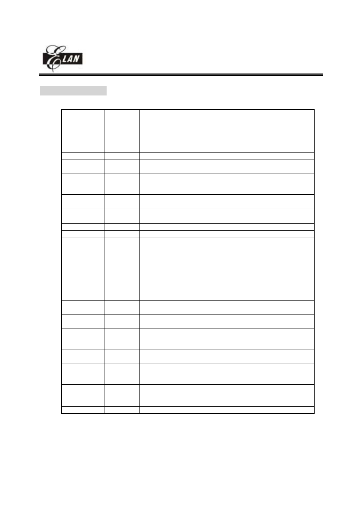
I.General Description
The EM78911 is an 8-bit CID (Call Identification) RISC type microprocessor with low power , high speed CMOS
technology . Integrated onto a single chip are on_chip watchdog (WDT) , RAM , ROM , programmable real time
clock /counter , internal interrupt , power down mode , LCD driver , FSK decoder ,CALL WAITING decoder, DTMF
generator and tri-state I/O . The EM78911 provides a single chip solution to design a CID of calling message_display .
II.Feature
CPU
•Opera t ing voltage range : 2.5V〜5.5V
•16K× 13 on chip ROM
•2.8K× 8 on chip RAM
•Up to 36 bi-directional tri-state I/O ports
•8 level stack for subroutine nesting
•8-bit real time clock/counter (TCC)
•Two sets of 8 bit counters can be interrupt sources
•Selective signal sources and trigger edges , and with overflow interrupt
•Programmable free running on chip watchdog timer
•99.9% single instruction cycle commands
•Four modes (internal clock 3.579MHz)
1. Sleep mode : CPU and 3.579MHz clock turn off, 32.768KHz clock turn off
2. Idle mode : CPU and 3.579MHz clock turn off, 32.768KHz clock turn on
3. Green mode : 3.579MHz clock turn off, CPU and 32.768KHz clock turn on
4. Normal mode : 3.579MHz clock turn on , CPU and 32.768KHz clock turn on
•Ring on voltage detector and low battery detector
•Input port wake up function
•9 interrupt source , 4 external , 5 internal
•100 pin QFP or chip
•Port key scan function
•Clock frequency 32.768KHz
•Eight R-option pins
CID
•Operation Volltage 3.5 〜6V for FSK
•Operation Volltage 2.5 〜6V for DTMF
•Bell 202 , V.23 FSK demodulator
•DTMF generator
•Ring detector on chip
CALL WAITING
•Operation Volltage 3.6 〜5.5V
•Compatible with Bellcore special report SR-TSV-002476
•Call-Waiting (2130Hz plus 2750Hz) Alert Signal Detector
•Good talkdown and talkoff performance
•Sensitivity compensated by adjusting input OP gain
LCD
•LCD operation voltage chosen by software
•Common driver pins : 16
•Segment driver pins : 60
•1/4 bias
Page 2

2
EM78911
EM78911EM78911
EM78911
88--bit micro
bit micro-
-controller
controller
•1/8,1/16 duty
III.Application
1. adjunct units
2. answering machines
3. feature phones
IV.Pin Configuration
Fig1. Pin Assignment
OTP writer PIN NAME MASK ROM PIN NAME P.S.
1.VDD VDD,AVDD
2.VPP /RESET
3.DINCK P77
4.ACLK P76
5.PGMB P75
6.OEB P74
7.DATA P73
8.GND VSS,AVSS
AVSS
DTMF
PLLC
RINGTIME
RDET1
RING
TIP
GAIN
CWTIP
XIN
XOUT
AVDD
COM7
COM6
COM5
COM4
COM3
COM2
COM1
COM0
SEG0
SEG1
SEG2
SEG3
SEG4
SEG5
SEG6
SEG7
SEG8
SEG9
SEG29
SEG28
SEG27
SEG26
SEG25
SEG24
SEG23
SEG22
SEG21
SEG20
SEG19
SEG18
SEG17
SEG16
SEG15
SEG14
SEG13
SEG12
SEG11
SEG10
SEG30
SEG31
SEG32
SEG33
SEG34
SEG35
SEG36
SEG37
SEG38
SEG39
VSS
TEST
COM8/P60
COM9/P61
COM10/P62
COM11/P63
COM12/P64
COM13/P65
COM14/P66
COM15/P67
SEG40/P54
SEG41/P55
SEG42/P56
SEG43/P57
SEG44/P80
SEG45/P81
SEG46/P82
SEG47/P83
SEG48/P84
SEG49/P85
SEG50/P86
SEG51/P87
SEG52/P90
SEG53/P91
SEG54/P92
SEG55/P93
SEG56/P94
SEG57/P95
SEG58/P96
SEG59/P97
P70/INT0
P71/INT1
P72/INT2
P73/INT3
P74
P75
P76
P77
/RESET
VDD
1234567891011121314151617181920212223242526272829
30
50
49
48
47
46
45
44
43
42
41
40
39
38
37
36
35
34
33
32
31
51
52
53
54
55
56
57
58
59
60
61
62
63
64
65
66
67
68
69
70
71
72
73
74
75
76
77
78
79
80
81
82
83
84
85
86
87
88
89
90
91
92
93
94
95
96
97
98
99
100
Page 3
3
EM78911
EM78911EM78911
EM78911
88--bit micro
bit micro-
-controller
controller
V.Functional Block Diagram
Fig2. Block diagram1
Fig3. Block diagram2
CPU
CPU
TIMING CONTROL
TIMING CONTROL
TIMER
TIMER
ROM
ROM
RAM
RAM
LCD DRIVER
LCD DRIVER
LCD
IO PORT
IO PORT I/O
FSK
DTMF
CALL WAITING
FSK
DTMF
CALL WAITING
Xin Xout
Oscillator
timing control
Control sleep
and wake-up
on I/O port
R1(TCC)
WDT timer
prescalar
GENERAL
RAM
R4
Interruption
control
ROM
Instruction
register
Instruction
decoder
R2
STACK
ALU
ACC
R3
R5
DATA & CONTROL BUS
2.5k RAM
PORT6
IOC6 R6
P60~P67
PORT7
IOC7 R7
P70~P77
PORT8
IOC8 R8
P80~P87
PORT9
IOC9 R9
P90~P97
PORT5
IOC5 R5
P54~P57
FSK
DTMF
CALL WAITING
Page 4
4
EM78911
EM78911EM78911
EM78911
88--bit micro
bit micro-
-controller
controller
VI.Pin Descriptions
PIN I/O DESCRIPTION
VDD
AVDD
POWER digital power
analog power
GND
AVSS
POWER digital ground
analog ground
Xtin I Input pin for 32.768 kHz oscillator
Xtout O Output pin for 32.768 kHz oscillator
COM0..COM7
COM8..COM15 O O (PORT6)
Common driver pins of LCD drivers
SEG0...SEG43
SEG44..SEG51
SEG52..SEG59
O
O (PORT8)
O (PORT9)
Segment driver pins of LCD drivers
PORT9 AS FUNCTION KEY CAN WAKE UP WATCHDOG.
PLLC I Phase loop lock capacitor, connect a capacitor 0.01u to 0.047u with
AVSS
TIP I Should be connected with TIP side of twisted pair lines for FSK.
RING I Should be connected with RING side of twisted pair lines for FSK.
CWTIP I Should be connected with TIP side of twisted pair lines for CW.
GAIN I OP output pin for gain adjustment.
RDET1 I Detect the energy on the twisted pair lines . These two pins coupled to
the twisted pair lines through an attenuating network.
/RING TIME I Determine if the incoming ring is valid.An RC network may be
connected to the pin.
INT0
INT1
INT2
INT3
PORT7(0)
PORT7(1)
PORT7(2)
PORT7(3)
PORT7(4:7)
PORT7(0)~PORT7(3) signal can be interrupt signals.
Int2 and int3 has the same interrupt flag.
IO port
P5.4 ~P5.7 PORT5 PORT 5 can be INPUT or OUTPUT port each bit.
Shared with LCD segment signals
P6.0 ~P6.7 PORT6 PORT 6 can be INPUT or OUTPUT port each bit.
Shared with LCD common signals
P7.0 ~P7.7 PORT7 PORT 7 can be INPUT or OUTPUT port each bit.
Internal Pul l high function.
Key scan function.
P8.0 ~P8.7 PORT8 PORT 8 can be INPUT or OUTPUT port each bit.
And shared with Segment signal.
P9.0 ~P9.7 PORT9 PORT 9 can be INPUT or OUTPUT port each bit.
And can be set to wake up watch dog timer.
And shared with Segment signal.
TEST I Test pin into test mode , normal low
DTMF O DTMF tone output
RESET I
Page 5
5
EM78911
EM78911EM78911
EM78911
88--bit micro
bit micro-
-controller
controller
VII.Functional Descriptions
VII.1 Operational Registers
1. R0 (Indirect Addressing Register)
* R0 is not a ph ysically imp lemented register. It is useful as indirect a ddressing p ointer. A ny instructio n using
R0 as register actually accesses data pointed by the RAM Select Register (R4).
2. R1 (TCC)
* Increased by an external signal edge applied to TCC , or by the instruction cycle clock.
Written and read by the program as any other register.
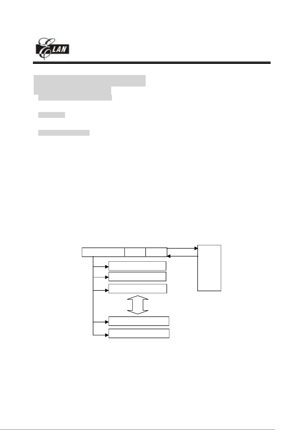
3. R2 (Program Counter)
* The structure is depicted in Fig. 4.
* Generates 16K × 13 on-chip ROM addresses to the relative programming instruction codes.
* "JMP" instruction allows the direct loading of the low 10 program counter bits.
* "CALL" instruction loads the low 10 bits of the PC, PC+1, and then push into the stack.
* "RET'' ("RETL k", "RETI") instruction loads the program counter with the contents at the top of stack.
* "MOV R2,A" allows the loading of an address from the A register to the PC, and the ninth and tenth bits are
cleared to "0''.
* "ADD R2,A" allows a relative address be added to the current PC, and contents of the ninth and tenth bits are
cleared to "0''.
* "TBL" allows a relative address be added to the current PC, and contents of the ninth and tenth bits don't
change. The most significant bit (A10~A13) will be loaded with the content of bit PS0~PS3 in the status register
(R5) upon the execution of a "JMP'', "CALL'', "ADD R2,A'', or "MOV R2,A'' instruction .
Fig.4 Program counter organization
PC
A13 A12 A11 A10 A9 A8 A7~A0
0000 PAGE0 0000~03FF
0001 PAGE1 0400~07FF
1110 PAGE14 3800~3BFF
1111 PAGE15 3C00~3FFF
0010 PAGE3 0800~0BFF
STACK1
STACK2
STACK3
STACK4
STACK5
STACK6
STACK7
STACK8
CALL
RET
RETL
RETI
Page 6
6
EM78911
EM78911EM78911
EM78911
88--bit micro
bit micro-
-controller
controller
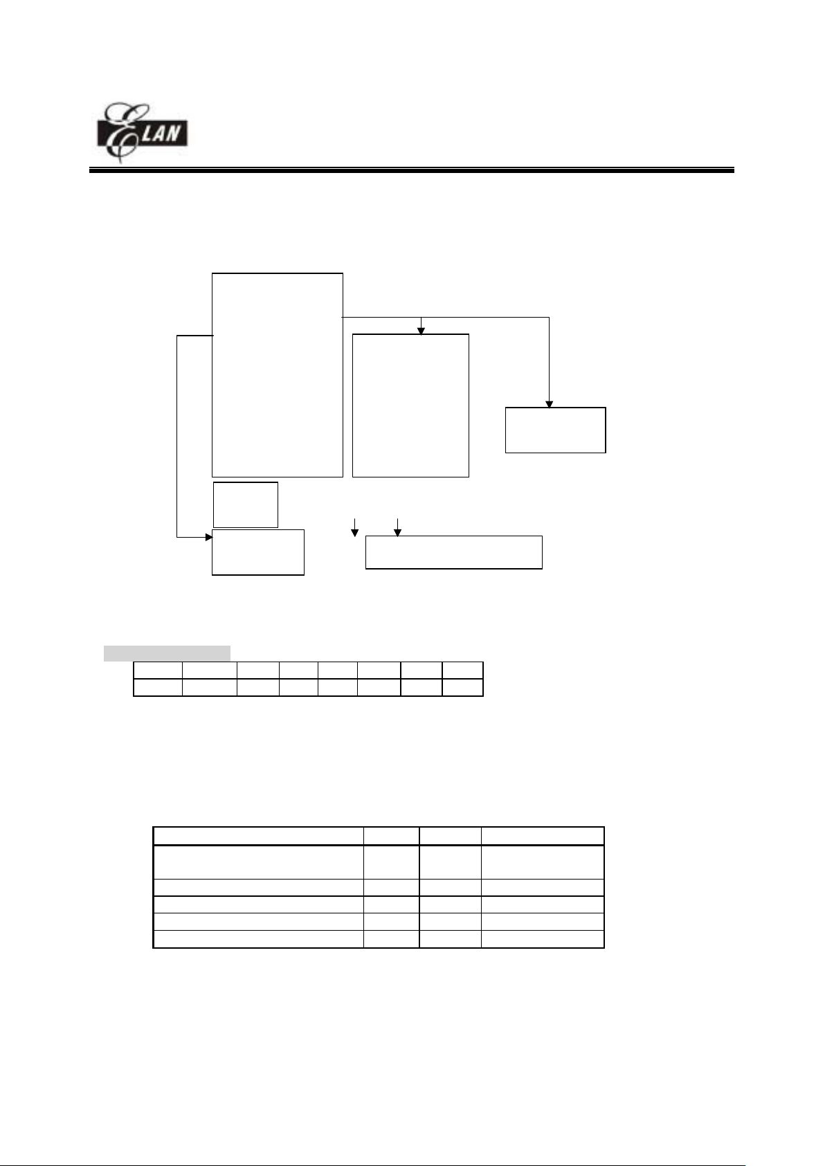
Fig.5 Data memory configuration
4. R3 (Status Register)
7 6 5 4 3 2 1 0
CAS PAGE - T P Z DC C
* Bit 0 (C) Carry flag
* Bit 1 (DC) Auxiliary carry flag
* Bit 2 (Z) Zero flag
* Bit 3 (P) Power down bit. Set to 1 during power on or by a "WDTC" command and reset to 0 by a "SLEP"
command.
* Bit 4 (T) Time-out bit. Set to 1 by the "SLEP" and "WDTC" command, or during power up and reset to 0 by
WDT timeout.
EVENT T P REMARK
WDT wake up from
sleep mode
0 0
WDT time out (not sleep mode) 0 1
/RESET wake up from sleep 1 0
power up 1 1
Low pulse on /RESET x x x .. don't care
* Bit 5 unused
* Bit 6 PAGE : change IOCB ~ IOCE to another page , 0/1 => page0 / page1
* Bit7 (CAS : CALL WAITING Output)
0/1= CW data valid/No data
00
01
02
03
04
05
06
07
08
09
0A
0B
0C
0D
0E
0F
R0
R1(TCC)
R2(PC)
R3(STATUS)
R4(RSR)
R5(ROM PAGE & R5)
R6(PORT6)
R7(PORT7)
R8(PORT8)
R9(PORT9)
RA(CLK,FSK)
RB(DTMF)
RC(2.5K RAM ADDRES S)
RD(2.5K RAM DATA)
RE(WDT)
RF(INT FLAG)
10
:
1F
16X8
COMMON
REGISTER
20
:
3F
BANK0 ~BANK3
32X8 ~32X8
REGISTER
IOC6
IOC7
IOC8
IOC9
IOCA
IOCB(LCD ADDRESS)
IOCC(LCD DATA)
IOCD(PULL HIGH)
IOCE(IO, LCD)
IOCF(INT CONTROL)
IOCB(COUNTER1)
IOCC(COUNTER2)
IOCD(R-OPTION)
page0
page1
BANK1 BANK2 …………..BANK10
256X8 256X8 …………….256X8
RC(ADDRESS) RD(DATA)
0
:
255
ADDRESS REGISTER CONTROL REGISTER
(PAGE0)
CONTROL REGISTER
(PAGE1)
Page 7
7
EM78911
EM78911EM78911
EM78911
88--bit micro
bit micro-
-controller
controller
5. R4 (RAM Select Register)
* Bits 0 ~ 5 are used to select up to 64 registers in the indirect addressing mode.
* Bits 6 ~ 7 determine which bank is activated among the 4 banks.
* See the configuration of the data memory in Fig. 5.
6. R5 (Program Page Select Register)
7 6 5 4 3 2 1 0
R57 R56 R55 R54
PS3 PS2 PS1 PS0
* Bit 0 (PS0) ~ 3 (PS3) Page select bits
Page select bits
PS3 PS2 PS1 PS0 Program memory page (Address)
0 0 0 0 Page 0
0 0 0 1 Page 1
0 0 1 0 Page 2
0 0 1 1 Page 3
0 1 0 0 Page 4
0 1 0 1 Page 5
0 1 1 0 Page 6
0 1 1 1 Page 7
1 0 0 0 Page 8
1 0 0 1 Page 9
1 0 1 0 Page 10
1 0 1 1 Page 11
1 1 0 0 Page 12
1 1 0 1 Page 13
1 1 1 0 Page 14
1 1 1 1 Page 15
*User can use PAGE instruction to change page. To maintain program page by user. Otherwise, user can use
far jump (FJMP) or far call (FCALL) instructions to program user's code. And the program page is
maintained by EMC's complier. It will change user's program by inserting instructions within program.
*Bit4~7 : PORT5 4-bit I/O register
6. R6 ~ R9 (Port 6 ~ Port 9)
* Four 8-bit I/O registers.
7. RA (FSK Status Register)(bit 0,1,2,4 read only)
7 6 5 4 3 2 1 0
IDLE
/358E /LPD /LOW_BAT /FSKPWR DATA /CD /RD
* Bit0 (Read Only) (Ring detect signal) 0/1 : Ring Valid/Ring Invalid
* Bit1(Read Only)(Carrier detect signal) 0/1 : Carrier Valid/Carrier Invalid
* Bit2(Read Only)(FSK demodulator output signal)
Fsk data transmitted in a baud rate 1200 Hz.
* Bit3(read/write)(FSK block power up signal)
1/0 : FSK demodulator block power up/FSK demodulator power down
Page 8
8
EM78911
EM78911EM78911
EM78911
88--bit micro
bit micro-
-controller
controller
* The relation between Bit0 to Bit3 is shown in Fig.6.
sleep mode
sleep modesleep mode
sleep mode
wake up
wake up wake up
wake up
mode
modemode
mode
/RINGTIME ='0'
/RINGTIME ='0'/RINGTIME ='0'
/RINGTIME ='0'
FSK decoder
FSK decoderFSK decoder
FSK decoder
begin its work
begin its workbegin its work
begin its work
/FSKPWR='1'
/FSKPWR='1'/FSKPWR='1'
/FSKPWR='1'
DATA transfer
DATA transfer DATA transfer
DATA transfer
to Micro
to Microto Micro
to Micro
/RD and /CD ='1' and
/RD and /CD ='1' and/RD and /CD ='1' and
/RD and /CD ='1' and
nothing to do for 30
nothing to do for 30 nothing to do for 30
nothing to do for 30
sec , /FSKPWR='0'
sec , /FSKPWR='0'sec , /FSKPWR='0'
sec , /FSKPWR='0'
or external keys
or external keysor external keys
or external keys
pressed
pressedpressed
pressed
/RD and /CD ='1'
/RD and /CD ='1'/RD and /CD ='1'
/RD and /CD ='1'
SLEEP MODE
SLEEP MODESLEEP MODE
SLEEP MODE
Begin
Begin Begin
Begin
set /FSKPWR='0'
set /FSKPWR='0'set /FSKPWR='0'
set /FSKPWR='0'
/RINGTIME ='0'
/RINGTIME ='0'/RINGTIME ='0'
/RINGTIME ='0'
or external keys
or external keysor external keys
or external keys
pressed
pressedpressed
pressed
WAKE UP MODE
WAKE UP MODEWAKE UP MODE
WAKE UP MODE
8-bit wake up and
8-bit wake up and 8-bit wake up and
8-bit wake up and
set /FSKPWR='1'
set /FSKPWR='1'set /FSKPWR='1'
set /FSKPWR='1'
accept data from
accept data fromaccept data from
accept data from
FSK decoder
FSK decoderFSK decoder
FSK decoder
/RD and /CD ='1'
/RD and /CD ='1'/RD and /CD ='1'
/RD and /CD ='1'
data end and 30
data end and 30data end and 30
data end and 30
sec nothing to do.
sec nothing to do.sec nothing to do.
sec nothing to do.
Yes
YesYes
Yes
No
NoNo
No
No
NoNo
No
Yes
YesYes
Yes
STATE Diagram between 8-bit
STATE Diagram between 8-bit STATE Diagram between 8-bit
STATE Diagram between 8-bit
and FSK decoder
and FSK decoderand FSK decoder
and FSK decoder
Flow Diagram between 8-bit
Flow Diagram between 8-bit Flow Diagram between 8-bit
Flow Diagram between 8-bit
and FSK decoder
and FSK decoderand FSK decoder
and FSK decoder
Fig6. The relation between Bit0 to Bit3.
* Bit4(Read Only)(Low battery signal) 0/1 = Battery voltage is low/Normal .
If the VDD voltage is under low power range (controlled by IOCA bit0) then sends a '0' signal to
/LOW_BAT bit or a '1' signal to this Bit.
* Bit5(read/Write)(Low battery detect enable)
0/1 = low battery detect DISABLE/ENABLE.
The relation between /LPD,/POVD and /LOW_BAT can see Fig7.
Vdd
VddVdd
Vdd
Vref
VrefVref
Vref
s2
s2s2
s2
1 on
1 on1 on
1 on
0 off
0 off0 off
0 off
s2
s2s2
s2
1 on
1 on1 on
1 on
0 off
0 off0 off
0 off
1 on
1 on1 on
1 on
to Low bat
to Low batto Low bat
to Low bat
To reset
To resetTo reset
To reset
/POVD
/POVD/POVD
/POVD
/LPD
/LPD/LPD
/LPD
/LPD
/LPD/LPD
/LPD
++++
----
1 on
1 on1 on
1 on
Fig7. The relation between /LPD,/POVD
* Bit6(read/write)(PLL enable signal)
0/1=DISABLE/ENABLE
The relation between 32.768K and 3.579M can see Fig8.
Fig8. The relation between 32.768K and 3.579K .
Sub-clock
32.768KH z
PLL
3.579M Hz
RA bit6 sw itch To system clock
1
0
Page 9
9
EM78911
EM78911EM78911
EM78911
88--bit micro
bit micro-
-controller
controller
* Bit7 IDLE: sleep mode selection bit
0/1=sleep mode/IDLE mode. This bit will decide SLEP instruction which mode to go.
These two modes can be waken up by TCC clock or Watch Dog or PORT9 and run from “SLEP” next
instruction.
Wakeup signal SLEEP mode IDLE mode GREEN mode NORMAL mode
RA(7,6)=(0,0)
+ SLEP
RA(7,6)=(1,0)
+ SLEP
RA(7,6)=(x,0)
no SLEP
RA(7,6)=(x,1)
no SLEP
TCC time out X Wake-up
+ Interrupt
+ Next instruction
Interrupt
Interrupt
WDT time out RESET Wake-up
+ Next instruction
RESET RESET
Port9
/RINGTIME pin
RESET Wake-up
+ Next instruction
X X
PORT70~73 X Wake-up
+ Interrupt
+ Next instruction
Interrupt
Interrupt
*P70 ~ P73 's wakeup function is co ntrolled by IOCF(1,2,3) and ENI instruction.
*P70 's wakeup signal is a rising or falling signal defined by CONT REGISTER bit7.
*/RINGTIME pin , Port9 ,Port71,Port72 and Port73 's wakeup signal is a falling edge signal.
8. RB(DTMF tone row and column register) (read/write)
7 6 5 4 3 2 1 0
c7 c6 c5 c4 r3 r2 r1 r0
* Bit 0 - Bit 3 are row-frequency tone.
* Bit 4 - Bit 7 are column-frequency tone.
* Initial RB is equal to high. Bit 7 ~ 0 are all " 1" , turn off DTMF power .
bit 3~0 Row freq
1110 699.2Hz 1 2 3 A
1101 771.6Hz 4 5 6 B
1011 854Hz 7 8 9 C
0111 940.1Hz * 0 # D
Column freq 1203Hz 1331.8Hz 1472Hz 1645.2Hz
bit 7~4 1110 1101 1011 0111
9. RC(CALLER ID address)(read/write)
7 6 5 4 3 2 1 0
CIDA7 CIDA6 CIDA5 CIDA4 CIDA3 CIDA2 CIDA1 CIDA0
* Bit 0 ~ Bit 7 select CALLER ID RAM address up to 256.
10. RD(CALLER ID RAM data)(read/write)
* Bit 0 ~ Bit 8 are CALLER ID RAM data transfer register.
User can see IOCA register how to select CID RAM banks.
Page 10
10
EM78911
EM78911EM78911
EM78911
88--bit micro
bit micro-
-controller
controller
11. RE(LCD Driver,WDT Control)(read/write)
7 6 5 4 3 2 1 0
CWPWR /WDTE /WUP9H /WUP9L /WURING LCD_C2 LCD_C1 LCD_M
* Bit0 (LCD_M):LCD_M decides the methods, including duty, bias, and frame frequency.
* Bit1~Bit2 (LCD_C#):LCD_C# decides the LCD display enable or blanking. change the display duty must set
the "LCD_C2,LCD_C1" to "00".
LCD_C2,LCD_C1 LCD Display Control LCD_M duty bias
0 0 change duty
Disable(turn off LCD)
0
1
1/16 1/4
1/8 1/4
0 1 Blanking : :
1 1 LCD display enable : :
* Bit3 (/WURING, RING Wake Up Enable): used to enable the wake-up function of /RINGTIME input pin.
(1/0=enable/disable)
* Bit4 (/WUP9L, PORT9 low nibble Wake Up Enable): used to enable the wake-up function of low nibble in
PORT9.(1/0=enable/disable)
* Bit5 (/WUP9H, PORT9 high nibble Wake Up Enable): used to enable the wake-up function of high nibble in
PORT9.(1/0=enable/disable)
* Bit6 (/WDTE,Watch Dog Timer Enable)
Control bit used to enable Watchdog timer.(1/0=enable/disable)
The relation between Bit3 to Bit6 can see the diagram 9.
* Bit7(Power control of Call Waiting circuit)
.(1/0=enable circuit /disable circuit) Please enable PLL before enable Call Waiting circuit.
/WURING
/WURING/WURING
/WURING
/RINGTIME
/RINGTIME/RINGTIME
/RINGTIME
/WUP9L
/WUP9L/WUP9L
/WUP9L
PORT9(3:0)
PORT9(3:0)PORT9(3:0)
PORT9(3:0)
/WUP9H
/WUP9H/WUP9H
/WUP9H
PORT9(7:4)
PORT9(7:4)PORT9(7:4)
PORT9(7:4)
/WDTE
/WDTE/WDTE
/WDTE
/WDTEN 0/1=enable/disable
/WDTEN 0/1=enable/disable/WDTEN 0/1=enable/disable
/WDTEN 0/1=enable/disable
fig.9 Wake up function and control signal
12. RF (Interrupt Status Register)
7 6 5 4 3 2 1 0
INT3 FSK/CW C8_2 C8_1 INT2 INT1 INT0 TCIF
* "1" means interrupt request, "0" means non-interrupt
* Bit 0 (TCIF) TCC timer overflow interrupt flag. Set when TCC timer overflows .
* Bit 1 (INT0) external INT0 pin interrupt flag .
* Bit 2 (INT1) external INT1 pin interrupt flag .
* Bit 3 (INT2) external INT2pin interrupt flag .
* Bit 4 (C8_1) internal 8 bit counter interrupt flag .
* Bit 5 (C8_2) internal 8 bit counter interrupt flag .
* Bit 6 ( FSK/CW ) FSK data or Call waiting data interrupt flag
* Bit 7 (INT3) external INT3 pin interrupt flag.
* High to low edge trigger , Refer to the Interrupt subsection.
* IOCF is the interrupt mask register. User can read and clear.
Page 11
11
EM78911
EM78911EM78911
EM78911
88--bit micro
bit micro-
-controller
controller
13. R10~R3F (General Purpose Register)
* R10~R3F (Banks 0~3) all are general purpose registers.
VII.2 Special Purpose Registers
1. A (Accumulator)
* Internal data transfer, or instruction operand holding
* It's not an addressable register.
2. CONT (Control Register)
7 6 5 4 3 2 1 0
INT_EDGE
INT TS TE PAB PSR2 PSR1 PSR0
* Bit 0 (PSR0) ~ Bit 2 (PSR2) TCC/WDT prescaler bits.
PSR2 PSR1 PSR0 TCC Rate WDT Rate
0 0 0 1:2 1:1
0 0 1 1:4 1:2
0 1 0 1:8 1:4
0 1 1 1:16 1:8
1 0 0 1:32 1:16
1 0 1 1:64 1:32
1 1 0 1:128 1:64
1 1 1 1:256 1:128
* Bit 3 (PAB) Prescaler assignment bit.
0/1 : TCC/WDT
* Bit 4 (TE) TCC signal edge
0: increment from low to high transition on TCC
1: increment from high to low transition on TCC
* Bit 5 (TS) TCC signal source
0: internal instruction cycle clock
1: 16.384KHz
* Bit 6 : (INT)
INT enable flag
0: interrupt masked by DISI or hardware interrupt
1: interrupt enabled by ENI/RETI instructions
* Bit 7 : INT_EDGE
0:P70 's interruption source is a rising edge signal.
1:P7 0 's interruption source is a falling edge signal.
* CONT register is readable and writable.
Page 12
12
EM78911
EM78911EM78911
EM78911
88--bit micro
bit micro-
-controller
controller
3. IOC5 (I/O Port Control Register)
7 6 5 4 3 2 1 0
IOC57 IOC56 IOC55 IOC54 0 0 0 P5S
* Bit0: P5S is switch register for I/O port or LCD signal switching.
0/1= normal I/O port/SEGMENT output .
* Bit1~3: unused
* Bit 4 to Bit7 are PORT5 I/O direction control registers.
* "1" put the relative I/O pin into high impedance, while "0" put the relative I/O pin as output.
4. IOC6 ~ IOC9 (I/O Port Control Register)
* four I/O direc tion control registers.
* "1" put the relative I/O pin into high impedance, while "0" put the relative I/O pin as output.
* User can see IOCB register how to switch to normal I/O port.
5. IOCA (CALLER ID RAM,IO ,PAGE Control Register)(read/write,initial "00000000")
7 6 5 4 3 2 1 0
P8SH P8SL 0 CALL_4 CALL_3 CALL_2 CALL_1 RANGE
* Bit0 : register to control low power detection range .
0/1=3.2V/3.6V
* Bit4~Bit1:"000" to "1001" are ten blocks of CALLER ID RAM area. User can use 2.5K RAM with RD
ram address.
* Bit 5 unused
* Bit6: port8 low nibble switch, 0/1= normal I/O port/SEGMENT output .
* Bit7: port8 high nibble switch , 0/1= normal I/O port/SEGMENT output
6. IOCB (LCD ADDRESS)
PAGE0 : Bit6 ~ Bit0 = LCDA6 ~ LCDA0
The LCD display data is stored in the data RAM . The relation of data area and COM/SEG pin is as below:
COM15 ~ COM8 COM7 ~ COM0
40H (Bit15 ~ Bit8) 00H (Bit7 ~ Bit0) SEG0
41H 01H SEG1
: : :
: : :
: : :
: : :
7AH 4AH SEG58
7BH 3BH SEG59
7CH 3CH Empty
: : :
7FH 3FH Empty
PAGE1 : 8 bit up-counter (COUNTER1) preset and read out register . ( write = preset ) . After a
interruption , it will count from “00”.
Page 13

13
EM78911
EM78911EM78911
EM78911
88--bit micro
bit micro-
-controller
controller
7. IOCC (LCD DATA)
PAGE0 : Bit7 ~ Bit0 = LCD RAM data register
PAGE1 : 8 bit up-counter (COUNTER2) p r eset and read o ut register . ( write = preset) After a interruption , it
will count from “00”.
8. IOCD (Pull-high Control Register)
PAGE0:
7 6 5 4 3 2 1 0
PH7 PH6 PH5 PH4 PH3 PH2 PH1 PH0
* Bit 0 ~ 7 (/PH#) Control bit used to enable the pull-high of PORT7(#) pin.
1: Enable internal pull-high
0: Disab le internal pull-high
PAGE1:
7 6 5 4 3 2 1 0
RO7 RO6 RO5 RO4 RO3 RO2 RO1 RO0
* Bit 7 ~ 0 (RO7~0) Control bit used to enable the R-OPTION of PORT97~PORT90 pin.
1: Enable
0: Disable
RO is used for R-OPTION . Setting RO to ‘1’ will enable the status of R-option pin (P90 ~ P97) to read by
controller. Clearing RO will disable R-option function. If the R-option function is used, user must connect
PORT9 pins to GND by 560K external register . If the register is connected/disconnected , the R9 will
read as “ 0/1” when RO is set to ‘1’.
9. IOCE (Bias,PLL Control Register)
PAGE0 :
7 6 5 4 3 2 1 0
P9SH P9SL P6S Bias3 Bias2 Bias1
0 SC
* Bit 0 :SC (SCAN KEY signal ) 0/1 = disable/enable. Once you enable this bit , all of the LCD signal will
have a low pulse during a common period. This pulse has 30us width. Please use the procedure to
implement the key scan function.
a. set port7 as input port
b. set IOCD page0 port7 pull high
c. enable scan key signal
d. Once push a key . Set RA(6)=1 and switch to normal mode.
e. Blank LCD. Disable scan key signal.
f. Set P6S =0. Port6 sent probe signal to port7 and read port7. Get the key.
g. Note!! A probe signal should be delay a instruction at least to another probe signal.
h. Set P6S =1. Port6 as LCD signal. Enable LCD.
Page 14

14
EM78911
EM78911EM78911
EM78911
88--bit micro
bit micro-
-controller
controller
Fig.10. Key scan circuit
Fig.11.key scan signal
* Bit 1 :PORT7 PULL HIGH register option. Please use default value.
P70P71P72P73
P60
P61
P62
P63
KEY1
KEY2
KEY5
KEY3
KEY4
com2
seg
vdd
v1
v2
v3
vlcd
Gnd
vdd
v1
v2
v3
vlcd
Gnd
30us
Page 15

15
EM78911
EM78911EM78911
EM78911
88--bit micro
bit micro-
-controller
controller
* Bit 2~4 (Bias1~Bias3) Control bits used to choose LCD operation voltage .
LCD operate voltage Vop (VDD 5V) VDD=5V
000
001
010
011
100
101
110
111
0.60VDD
0.66VDD
0.74VDD
0.82VDD
0.87VDD
0.93VDD
0.96VDD
1.00VDD
3.0V
3.3V
3.7V
4.0V
4.4V
4.7V
4.8V
5.0V
* Bit5:port6 switch , 0/1= normal I/O port/COMMON output
* Bit6:port9 low nibble switch , 0/1= normal I/O port/SEGMENT output . Bit7:port9 high nibble switch
PAGE1 :
7 6 5 4 3 2 1 0
OP77 OP76 C2S C1S PSC1 PSC0 CDRD 0
* Bit0: unused
* Bit1: cooked data or raw data select bit , 0/1 ==> cooked data/raw data
* Bit3~Bit2: counter1 prescaler , reset=(0,0)
(PSC1,PSC0) = (0,0)=>1:1 , (0,1)=>1:4 , (1,0)=>1:8 , (1,1)=>reserved
* Bit4:counter1 source , (0/1)=(32768Hz/3.579MHz if enable) scale=1:1
* Bit5:counter2 source , (0/1)=(32768Hz/3.579MHz if enable) scale=1:1
* Bit6:P76 opendrain control (0/1)=(disable/enable)
* Bit7:P77 opendrain control (0/1)=(disable/enable)
10. IOCF (Interrupt Mask Register)
7 6 5 4 3 2 1 0
INT3 FSK/CW C8_2 C8_1 INT2 INT1 INT0 TCIF
* Bit 0 ~ 7 interrupt enable bit.
0: disable interrupt
1: enable interrupt
* IOCF Register is readable and writable.
VII.3 TCC/WDT Prescaler
There is an 8-bit counter available as prescaler for the TCC or WDT. The prescaler is available for the TCC only or
WDT only at the same time.
• An 8 bit counter is available for TCC or WDT determined by the status of the bit 3 (PAB) of the CONT register.
• See the prescaler ratio in CONT register.
• Fig. 10 depicts the circuit diagram of TCC/WDT.
• Both TCC and prescaler will be cleared by instructions which write to TCC each time.
•
The prescaler will be cleared by the WDTC and SLEP instructions, when assigned to WDT mode.
Page 16

16
EM78911
EM78911EM78911
EM78911
88--bit micro
bit micro-
-controller
controller
•
The prescaler will not be cleared by SLEP instructions, when assigned to TCC mode.
Fig. 10 Block diagram of TCC WDT
VII.4 I/O Ports
The I/O registers, Port 6 ~ Port 9, are bi-directional tri-state I/O ports. Port 7 can be pulled-high internally by
software control. The I/O ports can be defined as "input" or "output" pins by the I/O control registers (IOC6 ~ IOC9 )
under program control. The I/O registers and I/O control registers are both readable and writable. The I/O interface
circuit is shown in Fig.11.
Fig. 11 The circuit of I/O port and I/O control register
16.38KHz
Page 17

17
EM78911
EM78911EM78911
EM78911
88--bit micro
bit micro-
-controller
controller
VII.5 RESET and Wake-up
The RESET can be caused by
(1) Power on reset, or Voltage detector
(2) WDT timeout. (if enabled and in GREEN or NORMAL mode)
Note that only Power on reset, or only Voltage de tector in Case(1) is e nabled in the syste m by CODE Option bit. I f
Voltage detector is disabled, Power on reset is selected in Case (1). Refer to Fig. 12.
Fig. 12 Block diagram of Reset of controller
Once the RESET occurs, the following functions are performed.
• The oscillator is running, or will be started.
• The Program Counter (R2) is set to all "0".
• When power on, the upper 3 bits of R3 and the upper 2 bits of R4 are cleared.
• The Watchdog timer and prescaler are cleared.
• The Watchdog timer is disabled.
• The CONT register is set to all "1"
• The other register (bit7..bit0)
R5 = PORT
IOC5 = "11110000"
R6 = PORT IOC6 = "11111111"
R7 = PORT IOC7 = "11111111"
R8 = PORT IOC8 = "11111111"
R9 = PORT IOC9 = "11111111"
RA = "x00x0xxx IOCA = "00000000"
RB = "11111111" Page0 IOCB = "00000000" Page1 IOCB = "00000000"
RC = "00000000" Page0 IOCC = "0xxxxxxx" Page1 IOCC = "00000000"
RD = "xxxxxxxx" Page0 IOCD = "00000000"
Page1 IOCD = “00000000”
RE = "00000000" Page0 IOCE = "00000000" Page1 IOCE = "00000000"
RF = "00000000" IOCF = "00000000"
The controller can be awakened from SLEEP mode or IDLE mode (execution of "SLEP" instruction, named
as SLEEP MODE or IDLE mode) by (1)TCC time out (2) WDT time-out (if enabled) or, (3) external input at
PORT9. The three cases will cause the controller wake up and run from next instruction. After wake-up , user
should control WATCH DOG in case of reset in GREEN mode or NORMAL mode. The last two should be open
Page 18

18
EM78911
EM78911EM78911
EM78911
88--bit micro
bit micro-
-controller
controller
RE register before into sleep mode or IDLE mode . The first one case will set a flag in RF bit0 .But it will not go to
address 0x08.
Page 19

19
EM78911
EM78911EM78911
EM78911
88--bit micro
bit micro-
-controller
controller
VII.6 Interrupt
The CALLER ID IC has internal interrupts whic h are falling edge triggered, as followed : TCC ti mer overflow
interrupt (internal) , two 8-bit counters overflow interrupt .
If these interrupt sources change signal from high to low , then RF register will generate '1' flag to
corresponding register if you enable IOCF register.
RF is t he interrupt status register which records the interrupt request in flag bit. IOCF is the interrupt mask
register. Global interrupt is enabled by ENI instruction and is disabled by DISI instruction. When one of the
interrupts (when enabled) generated, will cause the next instruction to be fetched from address 008H. Once in the
interrupt service routine the source of the interrupt can be determined by po lling the flag bits in t he RF register. The
interrupt flag bit must be cleared in software before leaving the interrupt service routine and enabling interrupts to
avoid recursive interrupts.
There are four external interrupt pins including INT0 , INT1 , INT2 , INT3 . And four internal interrupt
available.
Internal signals include TCC,CNT1,CNT2,FSK and CALL WAITING data. The last two will generate a
interrupt when the data trasient from high to low.
External interrupt INT0 , INT1 , INT2 , INT3 signals are from PORT7 bit0 to bit3 . If IOCF is enable then
these signal will cause interrupt , or these signals will be treated as general input data .
After reset, the next instruction will be fetched from address 000H and the instruction inturrept is 001H and the
hardware inturrept is 008H.
TCC will go to address 0x08 in GREEN mode or NORMAL mode after time out. And it will run next
instruction from “SLEP” instruction. These two cases will set a RF flag.
It is very important to save ACC,R3 and R5 when processing a interruption.
Address Instruction Note
0x08 DISI ;Disable interrupt
0x09 MOV A_BUFFER,A ;Save ACC
0x0A SWAP A_BUFFER
0x0B SWAPA 0x03 ;Save R3 status
0x0C MOV R3_BUFFER,A
0x0D MOV A,0x05 ;Save ROM page register
0x0E MOV R5_BUFFER,A
: :
: :
: MOV A,R5_BUFFER ;Return R5
: MOV 0X05,A
: SWAPA R3_BUFFER ;Return R3
: MOV 0X03,A
: SWAPA A_BUFFER ;Return ACC
: RETI
VII.7 Instruction Set
Instruction set has the following features:
(1). Every bit of any register can be set, cleared, or tested directly.
(2). The I/O register can be regarded as general register. That is, the same instruction can operates on I/O register.
Page 20

20
EM78911
EM78911EM78911
EM78911
88--bit micro
bit micro-
-controller
controller
The symbol "R" represents a register designator which specifies which one of the 64 registers (including
operational registers and general purpose registers) is to be utilized by the instruction. Bit s 6 and 7 in R4 determine
the selected register bank. "b'' represents a bit field designator which selects the number of the bit, located in the
register "R'', affected by the operation. "k'' represents an 8 or 10-bit constant or literal value.
INSTRUCTION BINARY
HEX
MNEMONIC OPERATION
STATUS
AFFECTE
D
0 0000 0000 0000 0000 NOP No Operation None
0 0000 0000 0001 0001 DAA Decimal Adjust A C
0 0000 0000 0010 0002 CONTW
A → CONT
None
0 0000 0000 0011 0003 SLEP
0 → WDT, Stop oscillator
T,P
0 0000 0000 0100 0004 WDTC
0 → WDT
T,P
0 0000 0000 rrrr 000r IOW R
A → IOCR
None
0 0000 0001 0000 0010 ENI Enable Interrupt None
0 0000 0001 0001 0011 DISI Disable Interrupt None
0 0000 0001 0010 0012 RET
[Top of Stack] → PC
None
0 0000 0001 0011 0013 RETI
[Top of Stack] → PC
Enable Interrupt
None
0 0000 0001 0100 0014 CONTR
CONT → A
None
0 0000 0001 rrrr 001r IOR R
IOCR → A
None
0 0000 0010 0000 0020 TBL
R2+A → R2 bits 9,10 do not
clear
Z,C,DC
0 0000 01rr rrrr 00rr MOV R,A
A → R
None
0 0000 1000 0000 0080 CLRA
0 → A
Z
0 0000 11rr rrrr 00rr CLR R
0 → R
Z
0 0001 00rr rrrr 01rr SUB A,R
R-A → A
Z,C,DC
0 0001 01rr rrrr 01rr SUB R,A
R-A → R
Z,C,DC
0 0001 10rr rrrr 01rr DECA R
R-1 → A
Z
0 0001 11rr rrrr 01rr DEC R
R-1 → R
Z
0 0010 00rr rrrr 02rr OR A,R
A ∨ VR → A
Z
0 0010 01rr rrrr 02rr OR R,A
A ∨ VR → R
Z
0 0010 10rr rrrr 02rr AND A,R
A & R → A
Z
0 0010 11rr rrrr 02rr AND R,A
A & R → R
Z
0 0011 00rr rrrr 03rr XOR A,R
A ⊕ R → A
Z
0 0011 01rr rrrr 03rr XOR R,A
A ⊕ R → R
Z
0 0011 10rr rrrr 03rr ADD A,R
A + R → A
Z,C,DC
0 0011 11rr rrrr 03rr ADD R,A
A + R → R
Z,C,DC
0 0100 00rr rrrr 04rr MOV A,R
R → A
Z
0 0100 01rr rrrr 04rr MOV R,R
R → R
Z
0 0100 10rr rrrr 04rr COMA R
/R → A
Z
0 0100 11rr rrrr 04rr COM R
/R → R
Z
0 0101 00rr rrrr 05rr INCA R
R+1 → A
Z
0 0101 01rr rrrr 05rr INC R
R+1 → R
Z
0 0101 10rr rrrr 05rr DJZA R
R-1 → A, skip if zero
None
0 0101 11rr rrrr 05rr DJZ R
R-1 → R, skip if zero
None
0 0110 00rr rrrr 06rr RRCA R
R(n) → A(n-1 )
R(0) → C, C → A(7)
C
0 0110 01rr rrrr 06rr RRC R
R
(n)
→ R(n-1)
C
Page 21

21
EM78911
EM78911EM78911
EM78911
88--bit micro
bit micro-
-controller
controller
R(0) → C, C → R(7)
0 0110 10rr rrrr 06rr RLCA R
R(n) → A(n+1)
R(7) → C, C → A(0)
C
0 0110 11rr rrrr 06rr RLC R
R(n) → R(n+1)
R(7) → C, C → R(0)
C
0 0111 00rr rrrr 07rr SWAPA R
R(0-3) → A(4-7)
R(4-7) → A(0-3)
None
0 0111 01rr rrrr 07rr SWAP R
R(0-3) ↔ R(4-7)
None
0 0111 10rr rrrr 07rr JZA R
R+1 → A, skip if zero
None
0 0111 11rr rrrr 07rr JZ R
R+1 → R, skip if zero
None
0 100b bbrr rrrr 0xxx BC R,b
0 → R(b)
None
0 101b bbrr rrrr 0xxx BS R,b
1 → R(b)
None
0 110b bbrr rrrr 0xxx JBC R,b if R(b)= 0, skip None
0 111b bbrr rrrr 0xxx JBS R,b if R(b) =1, skip None
1 00kk kkkk kkkk 1kkk CALL k
PC+1 → [SP]
(Page, k) → PC
None
1 01kk kkkk kkkk 1kkk JMP k
(Page, k) → PC
None
1 1000 kkkk kkkk 18kk MOV A,k
k → A
None
1 1001 kkkk kkkk 19kk OR A,k
A ∨ k → A
Z
1 1010 kkkk kkkk 1Akk AND A,k
A & k → A
Z
1 1011 kkkk kkkk 1Bkk XOR A,k
A ⊕ k → A
Z
1 1100 kkkk kkkk 1Ckk RETL k
k → A, [Top of Stack] → PC
None
1 1101 kkkk kkkk 1Dkk SUB A,k
k-A → A
Z,C,DC
1 1110 0000 0001 1E01 INT
PC+1 → [SP]
001H → PC
None
1 1110 1000 kkkk 1E8k PAGE k K->R5(3:0) None
1 1111 kkkk kkkk 1Fkk ADD A,k
k+A → A
Z,C,DC
VII.8 CODE Option Register
The CALLER ID IC has one CODE option register which is not part of the normal program memory. The
option bits cannot be accessed during normal program execution.
7 6 5 4 3 2 1 0
- - - - - - /POVD
MCLK
* Bit 0 : main clock selection. 0/1 = 3.58MHZ / 1.84MHZ
main clock selection. 0/1 = 3.58MHZ / 1.84MHZmain clock selection. 0/1 = 3.58MHZ / 1.84MHZ
main clock selection. 0/1 = 3.58MHZ / 1.84MHZ
* Bit 1 :(/POVD) : Power on voltage detector.
0: enable
1: disable
/POVD 2.2V reset power on reset Low power
detect without
reset
Low power detect
controlled by
RA(5)
sleep mode
current
1 no yes Yes Yes 1uA
0 yes yes Yes yes 15uA
* Bits 2~7 : unused, must be "0"s.
VII.9 FSK FUNCTION
Page 22

22
EM78911
EM78911EM78911
EM78911
88--bit micro
bit micro-
-controller
controller
VII.9.1 Functional Block Diagram
Fig13. FSK Block Diagram
VII.9.2 Function Descriptions
The CALLER ID IC is a CMOS device designed to support the Caller Number Deliver feature which is offered
by the Regional Bell Operating Companies.The FSK block comprises two paths: the signal path and the ring indicator
path. The signal path consist of an input differential buffer,a band pass filter, an FSK demodulator and a data valid
with carrier detect circuit. The ring detector path includes a clock generator, a ring detect circuit .
In a typical application, the ring detector maintains the line continuo usly while all other functions of the
chip are inhibited. If a ring signal is sent, the /RI NGTIME pin w ill has a low sig nal. User can use this signa l to
wake up whole chip or read /RD signal from RA register.
A /FSKPWR input is provided to act ivate the block regardless of the presence of a power ring sig nal. If
/FSKPWR is sent low, the FSK bloc k will power down whenever it detects a valid ring signal, it will pow er on
when /FSKPWR is high.
T he input buffer accepts a differential AC coupled input signal through the TIP and RING input and feeds this
signal to a band pass filter. Once the signal is filtered, the FSK demodulator decodes the information and sends it to a
post filter. The output data is then made available at DATA OUT pin. This data, as sent by the central office, includes
the header information (alternate "1" and "0") and 150 ms of marking which precedes the date , time and calling
number. If no data is present, the DATA OUT pin is held in a high state. This is accomplished by an carrier detect
circuit which determines if the in-band energy is high enough. If the incoming signal is valid and thus the
demodulated data is transferred to DATA OUT pin . If it is not, then the FSK demodulator is blocked.
VII.9.3 Ring detect circuit
When Vdd is applied to the circuit, the RC network will charge cap C1 to Vdd holding /RING TIME off .
The resistor network R2 to R3 attenuat es the incoming power ring applied to the top of R2 . The values given
Ring
Det
Circuit
Ring det1
Tip
Ring
Power
Up
FSK
demodul
Data Valid
Energy Det
Circuit
DATA OUT
/CD
CLOCK
OSC in
OSC out
/RD
/Ring Time
Band Pass
Filter
/FSKPWR
Page 23

23
EM78911
EM78911EM78911
EM78911
88--bit micro
bit micro-
-controller
controller
have been chosen to provide a sufficient voltage at DET1 pin, to turn on the Schmitt trigger input . When Vt+ of
the Schmitt is exceeded, cap C1 will discharge.
The value of R1 and C1 must be cho sen to hold the /RING TIME pin voltage below the Vt+ of the Schmitt
between the individual cycle of the power ring. With /RINGTIME enabled, this signal w ill be a /RD signal in
RA throught a buffer.
Fig14. ring detect circuit
VII.10 DTMF ( Dual Tone Multi Frequency ) Tone Generator
Built-in DTMF generator can generate dialing tone signals for telephone of dialing tone type. There are two
kinds of DTMF tone . One is the group of row frequency, the other is the group of column frequency, each group has
4 kinds of freq uency , user can get 16 kinds of DTMF frequency totally. D TMF generator contains a r ow frequency
sine wave generator for generating the DTMF signal which selected by low order 4 bits of RB and a column frequency
sine wave generator for generating the DTMF signal which selected by high order 4 bits of RB. This block can
generate single tone by filling one bit zero to this register.
If all the values are high , the power of DTMF will turn off until one or two low values.
Either high or low 4 bits must be set by an effective value, otherwise, if any ineffective value or both 4 bits are
load effective value, tone output will be disable. Recommend value refer to table as follow please :
SYSTEM CLOCK
SYSTEM CLOCKSYSTEM CLOCK
SYSTEM CLOCK
DTMF low-freq
DTMF low-freqDTMF low-freq
DTMF low-freq
selection
selectionselection
selection
DTMF high-freq
DTMF high-freqDTMF high-freq
DTMF high-freq
selection
selectionselection
selection
Sine wave
Sine wave Sine wave
Sine wave
generator
generatorgenerator
generator
Sine wave
Sine wave Sine wave
Sine wave
generator
generatorgenerator
generator
Adder
AdderAdder
Adder
ROW
ROWROW
ROW
Register
RegisterRegister
Register
COLUMN
COLUMNCOLUMN
COLUMN
Register
RegisterRegister
Register
Low frequency generator
Low frequency generatorLow frequency generator
Low frequency generator
High frequency generato
r
High frequency generato
r
High frequency generato
r
High frequency generato
r
DTMF to
ne
DTMF to
ne
DTMF to
ne
DTMF to
ne
output
outputoutput
output
Vdd
/Ring Time
Det1
/RD
C1
R3
R1
R2
/Ring Time
Page 24

24
EM78911
EM78911EM78911
EM78911
88--bit micro
bit micro-
-controller
controller
Fig15. DTMF Block Diagram
* RB ( DTMF Register )
. Bit 0 - Bit 3 are row-frequency tone.
. Bit 4 - Bit 7 are column-frequency tone.
. Initial RB is equal to HIGH.
. Except below values of RB ,the other values of RB are not effect. If RB is set by ineffective value, the DTMF
output will be disable and there is no tone output.
. Bit 7 ~ 0 are all "1" , turn off DTMF power .
bit 3~0 Row freq
1110 699.2Hz 1 2 3 A
1101 771.6Hz 4 5 6 B
1011 854Hz 7 8 9 C
0111 940.1Hz * 0 # D
Column freq 1203Hz 1331.8Hz 1472Hz 1645.2Hz
bit 7~4 1110 1101 1011 0111
VII.11 LCD Driver
The CALLER ID IC can drive LCD directly and has 60 segments and 16 commons that can drive 60*16 dots
totally. LCD block is made up of LCD driver , display RAM, segment output pins , common output pins and LCD
operating power supply pins.
Duty , bias , the number of segment , the number of common and frame frequency are determined by LCD
mode register . LCD control register.
The basic structure contains a timing control which uses the basic frequency 32.768KHz to generate the proper
timing for different duty and display access. RE register is a command register for LCD driver, the LCD
display( disable, enable, blanking) is controlled by LCD_C and the driving duty and bias is decided by LCD_M and
the display data is stored in data RAM which address and data access controlled by registers IOCB and IOCC.
Fig16. LCD DRIVER CONTROL
LCD timing control
RE(LCD_C,LCD_M)
Bias control
Vdd-Vlcd
LCD duty control
LCD COMMON control
COM
RAM
IOCB(address)
IOCC(data)
Display data control
LCD SEGMENT control
SEG
32.768KHz
Page 25

25
EM78911
EM78911EM78911
EM78911
88--bit micro
bit micro-
-controller
controller
VII.11.1 LCD Driver Control
RE(LCD Driver Control)(initial state "00000000")
7 6 5 4 3 2 1 0
- - - - - LCD_C2 LCD_C1 LCD_M
*Bit0 (LCD_M):LCD_M decides the methods, including duty, bias, and frame frequency.
*Bit1~Bit2 (LCD_C#):LCD_C# decides the LCD display enable or blanking. change the display duty must set
the LCD_C to "00".
LCD_C2,LCD_C1 LCD Display Control LCD_M duty bias
0 0 change duty
Disable(turn off LCD)
0
1
1/16 1/4
1/8 1/4
0 1 Blanking : :
1 1 LCD display enable : :
VII.11.2 LCD display area
The LCD display data is stored in the data RAM . The relation of data area and COM/SEG pin is as below:
COM15 ~ COM8 COM7 ~ COM0
40H (Bit15 ~ Bit8) 00H (Bit7 ~ Bit0) SEG0
41H 01H SEG1
: : :
: : :
7BH 3BH SEG59
7CH 3CH empty
7DH 3DH empty
7EH 3EH empty
7FH 3FH empty
*IOCB(LCD Display RAM address)
7 6 5 4 3 2 1 0
- LCDA6 LCDA5 LCDA4 LCDA3 LCDA2 LCDA1 LCDA0
Bit 0 ~ Bit 6 select LCD Display RAM address up to 120.
LCD RAM can be write whether in enable or disable mode and read only in disable mode.
*IOCC(LCD Display data) : Bit 0 ~ Bit 8 are LCD data.
VII.11.3 LCD COM and SEG signal
* COM signal : The number of COM pins varies according to the duty cycle used, as following: in 1/8 duty mode
COM8 ~ COM15 must be open. in 1/16 duty mode COM0 ~ COM15 pins must be used.
COM0 COM1 COM2 COM3 COM4 COM5 COM6 COM7 COM8 .. COM15
1/8 o o o o o o o o x .. x
1/16 o o o o o o o o o .. o
x:open,o:select
Page 26

26
EM78911
EM78911EM78911
EM78911
88--bit micro
bit micro-
-controller
controller
* SEG signal: The 60 segment signal pins are connected to the corresponding display RAM address 00h to 3Bh. The
high byte and the low byte bit7 down to bit0 are correlated to COM15 to COM0 respectively .
When a bit of display RAM is 1, a select signal is sent to the corresponding segment pin, and when the bit is 0 , a nonselect signal is sent to the corresponding segment pin.
*COM, SEG and Select/Non-select signal is shown as following:
Fig.17 Lcd wave 1/4 bias
Vdd
V1
V2
V3
VLCD
frame
com0
com1
com2
seg
seg
light
dark
Vdd
V1
V2
V3
VLCD
Vdd
V1
V2
V3
VLCD
Vdd
V1
V2
V3
VLCD
Vdd
V1
V2
V3
VLCD
Page 27

27
EM78911
EM78911EM78911
EM78911
88--bit micro
bit micro-
-controller
controller
VII.11.4 LCD Bias control
IOCE (Bias Control Register)
7 6 5 4 3 2 1 0
Bias3 Bias2 Bias1
* Bit 2~4 (Bias1~Bias3) Control bits used to choose LCD operation voltage . The circuit can refer ti figure15.
LCD operate voltage Vop (VDD 5V) VDD=5V
000
001
010
011
100
101
110
111
0.60VDD
0.66VDD
0.74VDD
0.82VDD
0.87VDD
0.93VDD
0.96VDD
1.00VDD
3.0V
3.3V
3.7V
4.0V
4.4V
4.7V
4.8V
5.0V
* Bit 5~7 unused
78810/78910
78810/7891078810/78910
78810/78910
Vdd
VddVdd
Vdd
Vlcd
VlcdVlcd
Vlcd
Vop
VopVop
Vop
Vss
VssVss
Vss
Vop=Vdd-Vlcd
Vop=Vdd-VlcdVop=Vdd-Vlcd
Vop=Vdd-Vlcd
R=1K
R=1KR=1K
R=1K
RRRR
RRRR
RRRR
RRRR
V1
V1V1
V1
V2
V2V2
V2
V3
V3V3
V3
MUX
Bias3~1
000
001
010
011
100
101
110
111
:
:
8.2R
0.4R
0.4R
0.3R
0.3R
0.2R
0.1R
0.1R
Fig.18 LCD bias circuit
Page 28

28
EM78911
EM78911EM78911
EM78911
88--bit micro
bit micro-
-controller
controller
VII.12 CALL WAITING Function Description
Fig.19 Call Waiting Block Diagram
Call Waiting service works by alerting a customer engaged in a telephon e call to a new
incoming call. This way the customer can still receive important calls while engaged in a
current call. The CALL WAITING DECODER can detect CAS(Call-Waiting Alerting Signal
2130Hz plus 2750Hz) and generate a valid signal on the data pins.
The call waiting decoder is designed to support the Caller Number Deliver feature, which
is offered by regional Bell Operating Companies. The call waiting decoder has four blocks,
including pre-amplifier, band pass filter, level detect and digital detection algorithm.
In a typical application, after enabling CW circuit (by RE BIT7 CWPWR) this IC receives
Tip and Ring signals from twisted pairs. The signals as inputs of pre-amplifier, and the
amplifier sends input signal to a band pass filter. Once the signal is filtered, the digital
detection block decodes the information and sends it to R3 register bit7 . The output data mad e
available at R3 CAS bit.
The data is CAS signals. The CAS is normal high. When this IC detects 2130Hz and
2750Hz frequency, then CAS pin goes to low.
CWTIP
Filter
Digital
Detection
Algorithm
Vdd/2
Band
Pass
Detect
Level
Voltage
Reference
Clock
Generator
GAIN
CAS
0: DATA valid
1: DATA invalid
call waiting circuit power control
FSK BLOCK
TIP
RING
+
FSK data
Page 29

29
EM78911
EM78911EM78911
EM78911
88--bit micro
bit micro-
-controller
controller
VIII.Absolute Operation Maximum Ratings
RATING SYMBOL VALUE UNIT
DC SUPPLY VOLTAGE Vdd -0.3 To 6 V
INPUT VOLTAGE Vin -0.5 TO Vdd +0.5 V
OPERATING TEMPERATURE RANGE Ta 0 TO 70
℃
IX DC Electrical Characteristic
(Ta=0°C ~ 70°C, VDD=5V±5%, VSS=0V)
(VDD=2.5V to 6 V for CPU ; VDD=3.5V to 6V for FSK ; VDD=2.5V to 6V for DTMF )
Symbol Parameter Condition Min Typ Max Unit
IIL1 Input Leakage Current for
input pins
VIN = VDD, VSS
±1 µA
IIL2 Input Leakage Current for
bi-directional pins
VIN = VDD, VSS
±1 µA
VIH Input High Voltage 2.5 V
VIL Input Low Voltage 0.8 V
VIHT Input High Threshold
Voltage
/RESET, TCC, RDET1 2.0 V
VILT Input Low Threshold
Voltage
/RESET, TCC,RDET1 0.8 V
VIHX Clock Input High Voltage OSCI 3.5 V
VILX Clock Input Low Voltage OSCI 1.5 V
VHscan Key scan Input High Voltage Port6 for key scan 3.5 V
VLscan Key scan Input Low Voltage Port6 for key scan 1.5 V
VOH1 Output High Voltage
(port6,7,8)
IOH = -1.6mA 2 . 4 V
(port9) IOH = -6.0mA 2.4 V
VOL1 Output Low Voltage
(port6,7,8)
IOL = 1.6mA 0.4 V
(port9) IOL = 6.0mA 0.4 V
Vcom Com voltage drop Io=+/- 50 uA - - 2.9 V
Vseg Segment voltage drop Io=+/- 50 uA - - 3.8 V
Vlcd LCD drive reference voltage Contrast adjustment
IPH Pull-high current Pull-high active input pin
at VSS
-10 -15
µµµµA
ISB1 Power down current
(SLEEP mode)
All input and I/O pin at
VDD, output pin floating,
WDT disabled
1 4
µA
ISB2 Low clock current
(GREEN mode)
CLK=32.768KHz, FSK,
DTMF, CW block disable ,
All input and I/O pin at
VDD, output pin floating,
WDT disabled, LCD enable
65 80
µA
ISB3 Low clock current
(IDLE mode)
CLK=32.768KHz, FSK,
DTMF, CW block disable ,
All input and I/O pin at
VDD, output pin floating,
WDT disabled, LCD enable
45 60
µA
Page 30

30
EM78911
EM78911EM78911
EM78911
88--bit micro
bit micro-
-controller
controller
CPU disable
ICC Operating supply current
(NORMAL mode)
/RESET=High,
CLK=3.579MHz, output pin
floating,LCD enable, FSK,
DTMF, CW Fblock disable
1.5 1.8 mA
IX AC Electrical Characteristic
(Ta=0°C ~ 70°C, VDD=5V, VSS=0V)
Symbol
Parameter Conditions
Min Typ Max Unit
Dclk
Input CLK duty cycle
45 50 55 %
Tins
Instruction cycle time 32.768K
3.579M
60
550
us
ns
Tdrh
Device delay hold time
18 ms
Ttcc
TCC input period Note 1
(Tins+20)/N ns
Twdt
Watchdog timer period
Ta = 25°C
18 ms
Note 1: N= selected prescaler ratio.
(FSK B a nd Pass Filter AC Characteristic)(Vdd=+5V,Ta=+25℃)
CHARACTERISTIC MIN TYP MAX UNIT
input sensitivity TIP and RING
pin1 and pin2 Vdd=+5V
-40 -48 -- dBm
(call waiting Band Pass Filter AC Characteristic)
(VDD=+5V,Ta=+25°C)
CHARACTERISTIC MIN TYP MAX UNIT
input sensitivity TIP and RING pins ,Vdd=+5V, Input G=1 -38 dBm
Description Symbol Min Typ Max Unit
OSC start up(32.768KHz)
(3.579MHz PLL)
Tosc -- 300 400
10
ms
(FSK AC Characteristic)
Carrier detect low Tcdl -- 10 14 ms
Data out to Carrier det low Tdoc -- 10 20 ns
Power up to FSK( setup time) Tsup -- 15 20 ms
/RD low to Ringtime low Trd 50 ms
End of FSK to Carrier Detect high Tcdh 8 -- -- ms
(Call waiting AC Characteristic)
CAS input signal length
(2130 ,2750 Hz @ -20dBm )
Tcasi 80 ms
Data detect delay time
Td 42 ms
Data release time
Tr 26 ms
Page 31

31
EM78911
EM78911EM78911
EM78911
88--bit micro
bit micro-
-controller
controller
XI. Timing Diagrams
`
LQV
Fig.20 AC timing
Page 32

32
EM78911
EM78911EM78911
EM78911
88--bit micro
bit micro-
-controller
controller
Fig.21 FSK Timing Diagram
Fig.22 Call Waiting Timing Diagram
PCW
Power
power off
power on
on/off
events
Td
plug in
on hook
in use
CAS
Tcasi
CAS
Tr
normal
TIP/RING
/RING TIME
/RD
/CD
DATA
OSC
FIRST RING
2 SECONDS
0.5 SEC
0.5 SEC
SECOND RING
2 SECONDS
DATA
3.579 MHz
Tcdl
/358E
Tosc
Tdoc
Tpd
Tsup
Tcdh
Trd
Page 33

33
EM78911
EM78911EM78911
EM78911
88--bit micro
bit micro-
-controller
controller
XII. Application Circuit
Fig23. APPLICATION CIRCUIT
1 2 34
A
B
C
D
4
321
D
C
B
A
Title
Number RevisionSize
A
Date: 18-May-1999 Sheet of
File: C:\ADVSCH\78911_1.SCH Drawn By:
TIP
RING
DET1
RINGTIME
AVSS
VSS
TEST
CWTIP
GAIN
COMMON
SEGMENT
AVDD
VDD
EST
ST/GT
PLLC
XIN
XOUT
RESET
LCD DISPLAY
0.22u
270K
VDD
470K
33K
10K
10K
300K
100
32768
0.01u
27
0.1u
0.1u
0.1u 250V
0.1u 250V
FUSE
1000P
1000P
TIP
RING
TO PHONE
VSS
DET1
VDD
VSS
AVSS
VSS
27
100K
100K
470K
NPN
0.1u
VDD
MATCHING NETWORK
10K
10K
103
Page 34

34
EM78911
EM78911EM78911
EM78911
88--bit micro
bit micro-
-controller
controller
附錄: EM78R911 SPEC.
IV.Pin Configuration
Fig1. Pin Assignment
1
2
3
4
5
6
7
8
9
10
11
12
13
14
15
16
17
18
19
20
21
22
23
24
25
26
27
28
29
30
31
32
33
34
35
36
37
38
39
40
80
79
78
77
76
75
74
73
72
71
70
69
68
67
66
65
64
63
62
61
60
59
58
57
56
55
54
53
52
51
50
49
48
47
46
45
44
43
42
41
120
119
118
117
116
115
114
113
112
111
110
109
108
107
106
105
104
103
102
101
100
99
98
97
96
95
94
93
92
91
90
89
88
87
86
85
84
83
82
81
121
122
123
124
125
126
127
128
129
130
131
132
133
134
135
136
137
138
139
140
141
142
143
144
145
146
147
148
149
150
151
152
153
154
155
156
157
158
159
160
SEG40
SEG41
SEG42
SEG43
TEST
P80
P81
P82
P83
P84
P85
P86
P87
P90
P91
P92
P93
P94
P95
P96
P97
VDD
NC
GND
IOD0
IOD1
IOD2
IOD3
IOD4
IOD5
IOD6
IOD7
INSEND
IRSEL
PH1OUT
X2OUT
/HOLD
/POVD
ENTCC
MCLK
NC
SEG39
SEG38
SEG37
SEG36
RESET
P77
P76
P75
P74
P73
P72
P71
P70
P67
P66
P65
P64
P63
P62
P61
P60
GND
NC
VDD
COM7
COM6
COM5
COM4
COM3
VSS2
COM2
COM1
COM0
SEG35
SEG34
SEG33
SEG32
SEG31
NC
SEG30
SEG29
SEG28
SEG27
SEG26
SEG25
SEG24
SEG23
SEG22
SEG21
SEG20
GND
NC
VDD
CD12
CD11
CD10
CD9
CD8
CD7
CD6
CD5
CD4
CD3
CD2
CD1
CD0
CA13
CA12
CA11
CA10
CA9
CA8
CA7
CA6
CA5
CA4
CA3
CA2
CA1
NC
AVSS
DTMF
PLLC
RINGTIME
RDET1
RING
TIP
CWRING
GAIN
XIN
XOUT
AVDD
SEG0
SEG1
SEG2
SEG3
SEG4
SEG5
SEG6
SEG7
SEG8
SEG9
VDD
NC
GND
SE10
SE11
SE12
SE13
SE14
SE15
SE16
VDD2
SE17
SE18
SE19
EPS
CA-1
CA0
Page 35

35
EM78911
EM78911EM78911
EM78911
88--bit micro
bit micro-
-controller
controller
VI.Pin Descriptions
PIN I/O DESCRIPTION
VDD1,VDD2
AVDD
POWER digital power
analog power
VSS1,VSS2
AVSS
POWER digital ground
analog ground
Xtin I Input pin for 32.768 kHz oscillator
Xtout O Output pin for 32.768 kHz oscillator
COM0..COM7
COM8..COM15
O
O (PORT6)
Common driver pins of LCD drivers
SEG0...SEG43
SEG44..SEG51
SEG52..SEG59
O
O (PORT8)
O (PORT9)
Segment driver pins of LCD drivers
PORT9 AS FUNCTION KEY CAN WAKE UP WATCHDOG.
PLLC I Phase loop lock capacitor
TIP I Should be connected with TIP side of twisted pair lines
RING I Should be connected with TIP side of twisted pair lines
CWTIP I Should be connected with TIP side of twisted pair lines for CW.
GAIN I OP output pin for gain adjustment.
RDET1 I Detect the energy on the twisted pair lines . These two pins coupled to
the twisted pair lines through an attenuating network.
/RING TIME I Determine if the incoming ring is valid.An RC network may be
connected to the pin.
INT0
INT1
INT2
INT3
PORT7(0)
PORT7(1)
PORT7(2)
PORT7(3)
PORT7(4:7)
PORT7(0)~PORT7(3) signal can be interrupt signals.
Int2 and int3 has the same interrupt flag.
IO port
P5.4 ~P7.7 PORT5 PORT 5 can be INPUT or OUTPUT port each bit.
Shared with LCD segment signals
P6.0 ~P6.7 PORT6 PORT 6 can be INPUT or OUTPUT port each bit.
Shared with LCD common signals
P7.0 ~P7.7 PORT7 PORT 7 can be INPUT or OUTPUT port each bit.
Internal Pul l high function.
Key scan function.
P8.0 ~P8.7 PORT8 PORT 8 can be INPUT or OUTPUT port each bit.
And shared with Segment signal.
P9.0 ~P9.7 PORT9 PORT 9 can be INPUT or OUTPUT port each bit.
And can be set to wake up watch dog timer.
And shared with Segment signal.
TEST I Test pin into test mode , normal low
DTMF O DTMF tone output
RESET I
X2OUT O System clock output.
CA-1
O CA-1 is used as address li ne to select low-order data (8 bits, through
CD0~CD7) or high-order data (5 bits, thr ough CD0~CD4)
ERS=1 => CA-1 NO USE
ERS=0 => CA-1=0 HIGH ORDER DATA
Page 36

36
EM78911
EM78911EM78911
EM78911
88--bit micro
bit micro-
-controller
controller
CA-1=1 LOW ORDER DATA
ERS I Input pin used to select the external ROM data bus through bus
CD0~D12 or CD0~CD7 only. HIGH/LOW = CD0~CD12 /
CD0~CD7.
ENTCC I
TCC control pin with internal pull-high (560KΩΩΩΩ). TCC works
normally when ENTCC is high, and TCC counting is stopped when
ENTCC is low.
CA0~CA13 O Program code address bus. CA0~CA13 are address output pins for
external programming ROM access.
CD0~CD12 I Data access in terms of CA0 ~ CA12 addressing.
IRSEL O IRSEL is an output pin used to select an external EVEN/ODD ROM.
INSEND O Used to indicate the instruction completion and ready for next
instruction.
/HOLD I Microcontroller hold request.
/POVD I Input pin used to enable Power on voltage detector. Power on voltage
detector is enabled if /POVD is low and is disabled if /POVD is high.
MCLK I Input pin for main clock selection. Internal pull low through a
register.
RC4M O RC clock for program down load
4MPD I RC 4M power control pin. This pin pull low internally to enable
clock. To pull high externally for disabling clock.
IOD0~IOD7 O I/O data bus.
PH1OUT O Phase 1 output
IX AC Electrical Characteristic
Tdiea Delay from Phase 3 end to
INSEND active
Cl=100pF 30 ns
Tdiei Delay from Phase 4 end to
INSEND inactive
Cl=100pF 30 ns
Tiew INSEND pulse width 30 ns
Tdca Delay from Phase 4 end to
CA Bus valid
C1=100pF 30 ns
Tacc ROM data access time 100 ns
Tcds ROM data setup time 20 ns
Tcdh ROM data hold time 20 ns
Tdca-1 Delay time of CA-1 C1=100pF 30 ns
Note 1: N= selected prescaler ratio.
Page 37

37
EM78911
EM78911EM78911
EM78911
88--bit micro
bit micro-
-controller
controller
CLK
341234 12 3
/INSEND
Tdiea Tdiei
Tiew
Tdca
CA13:0
Tacc
Tcds
CD12:0
Tcdh
CLK
341234 12 3
/INSEND
Tdiea Tdiei
Tiew
Tdca
CA13:0
Tacc
Tcds
CD7:0
Tcdh
CA-1
HIGH ORDER
DATA
LOW ORDER
DATA
EPS=0 CA-1=0 HIGH ORDER DATA CA-1=1 LOW ORDER DATA
EPS=1 CA-1=DISABLE
Tdca-1
 Loading...