

Page 1

1
* This specification are subject to be changed without notice.
12.17.2001
EM73P361AEM73P361A
EM73P361AEM73P361A
EM73P361A
4-BIT MICRO-CONTROLLER FOR LCD PRODUCT4-BIT MICRO-CONTROLLER FOR LCD PRODUCT
4-BIT MICRO-CONTROLLER FOR LCD PRODUCT4-BIT MICRO-CONTROLLER FOR LCD PRODUCT
4-BIT MICRO-CONTROLLER FOR LCD PRODUCT
GENERAL DESCRIPTIONGENERAL DESCRIPTION
GENERAL DESCRIPTIONGENERAL DESCRIPTION
GENERAL DESCRIPTION
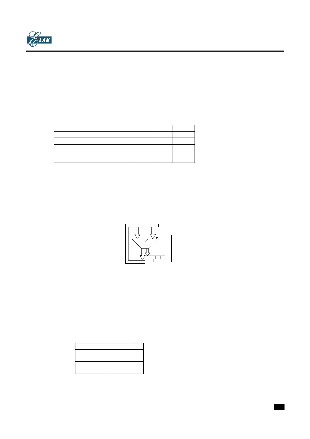
EM73P361A is an advanced single chip CMOS 4-bit one-time programming (OTP) micro-controller. It contains
3K-byte OTP ROM, 52-nibble RAM, 4-bit ALU, 13-level subroutine nesting, 22-stage time base, two 12-bit timer/
counters for the kernel function. EM73P361A also contains 5 interrupt sources, 1 input port, 4 bidirection I/O ports,
built-in watch-dog-timer counter, tone generator and LCD driver (27x3 to 13x3).
Except low-power consumption and high speed, EM73P361A also have a sleep mode operation for power saving.
FEATURESFEATURES
FEATURESFEATURES
FEATURES
• Operation voltage : 2.4V to 3.6V(clock frequency : 32K Hz).
• Clock source : Single clock system for crystal, connect a external resistor or external clock
source available by mask option.
• Instruction set : 109 powerful instructions.
• Instruction cycle time : 122µs for 32K Hz.
• OTP ROM capacity : 3072 x 8 bits.
• RAM capacity : 52 x 4 bits.
• Input port : 1 port (P0)(Pull-up and pull-down resistor with wakeup function available by
mask option).
• Bidirection port : 4 ports (P4, P5, P6, P7) are available by mask option. (each I/O pin is push-pull
and open-drain available by mask option) P4.0 is high current pin (P4.0 and
TONE available by mask option). P4.2~P4.3, P5, P6 and P7 are shared with
SEG26-SEG13 by mask option.
• 12-bit timer/counter : Two 12-bit timer/counters are programmable for timer mode.
• Low voltage reset (LVR) : Reset at 2.2V, and reset release at 2.4V.
• Tone generator : There is a built-in tone generator.
• Built-in time base counter : 22 stages.
• Subroutine nesting : Up to 13 levels.
• Interrupt : External . . . . . 2 External interrupt (INT0, INT1).
Internal . . . . . . 2 Timer overflow interrupts.
1 Time base interrupt.
• LCD driver : 27 X 3 to 13 X 3 dots available by mask option. Capacitor divider and resistor
divider are available by mask option.1/3, 1/2 and static three kinds of duty (1/2
bias) selectable. The programming method of LCD driver is I/O mapping.
• Built-in watch-dog-timer : The WDT is enabled or disabled by mask option.
• Power saving function : Sleep mode and Hold mode.
• Package type : EM73P361AH Chip form 47 pins.
EM73P361AAQ QFP 100 pins.
APPLICATIONSAPPLICATIONS
APPLICATIONSAPPLICATIONS
APPLICATIONS
EM73P361A is suitable for application in family appliance, consumer products, hand held games and the toy
controller.
Page 2
2
* This specification are subject to be changed without notice.
12.17.2001
EM73P361AEM73P361A
EM73P361AEM73P361A
EM73P361A
4-BIT MICRO-CONTROLLER FOR LCD PRODUCT4-BIT MICRO-CONTROLLER FOR LCD PRODUCT
4-BIT MICRO-CONTROLLER FOR LCD PRODUCT4-BIT MICRO-CONTROLLER FOR LCD PRODUCT
4-BIT MICRO-CONTROLLER FOR LCD PRODUCT
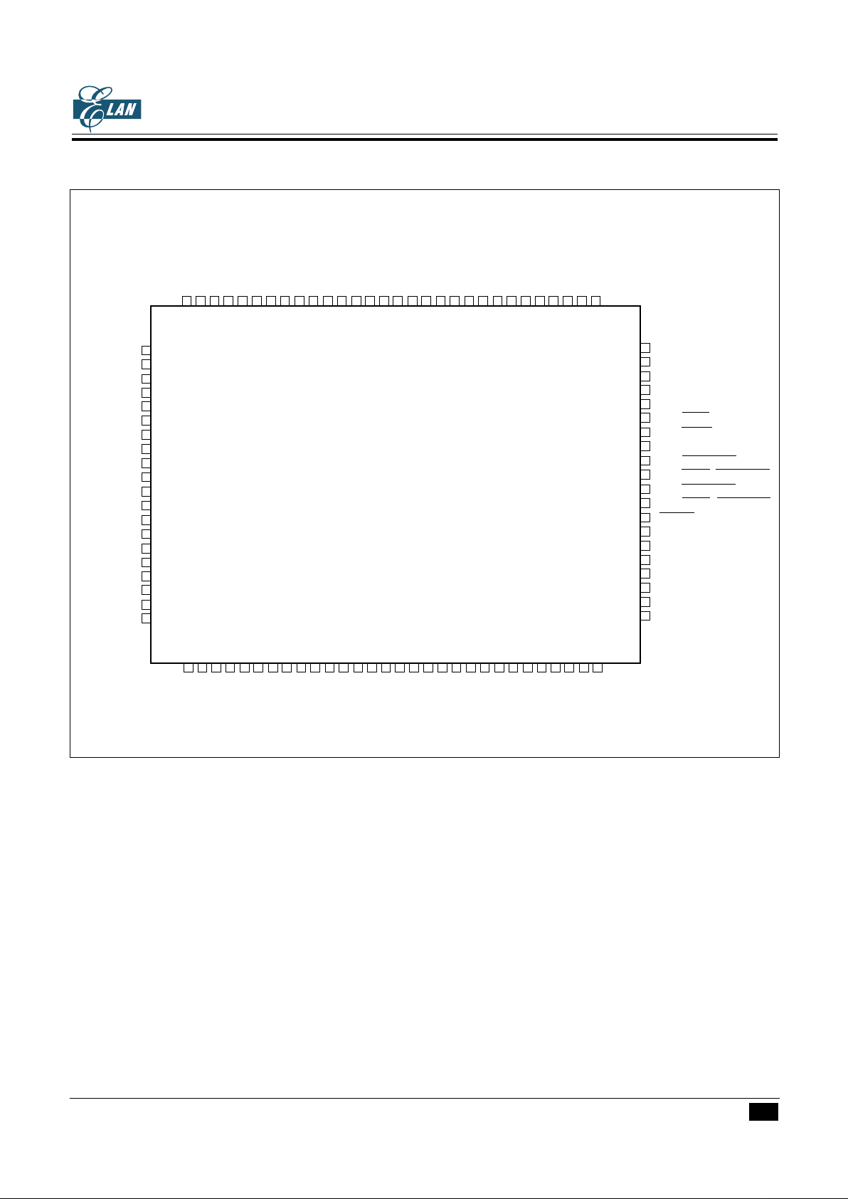
PIN CONFIGURATIONSPIN CONFIGURATIONS
PIN CONFIGURATIONSPIN CONFIGURATIONS
PIN CONFIGURATIONS
123456789
101112131415161718192021222324252627282930
50
49
48
47
46
45
44
43
42
41
40
39
38
37
36
35
34
33
32
31
8079787776757473727170696867666564636261605958575655545352
51
81
82
83
84
85
86
87
88
89
90
91
92
93
94
95
96
97
98
99
100
NC
NC
NC
NC
P7.1/SEG15
P7.2/SEG14
P7.3/SEG13
SEG12
SEG11
SEG10
SEG9
SEG8
SEG7
SEG6
SEG5
SEG4
SEG3
NC
NC
NC
NCNCNCNCNCNCNC
NC
SEG2
SEG1
SEG0
COM1
COM0
VEE
VB
VA
XIN
XOUT
NCNCNCNCNCNCNCNCNC
NC
NC
NC
NC
NC
P4.1/WDT
P4.0/TONE
TONE
P0.3/WAKEUP3
P0.2(INT0)/WAKEUP2
P0.1/WAKEUP1
P0.0(INT1)/WAKEUP0
RESET
NC
NC
NC
NC
NCNCNCNCNC
NC
TEST
VPPNCNCNCNCNCNCNCNC
NC
EM73P361AAQ
QFP 100
NC
NC
NC
NC
VDD
VSS
P4.3/SEG25
P4.2/SEG26
COM2
P5.0/SEG24
P5.2/SEG22
P5.1/SEG23
P6.0/SEG20
P5.3/SEG21
P6.2/SEG18
P6.1/SEG19
P7.0/SEG16
P6.3/SEG17
NC
Page 3
3
* This specification are subject to be changed without notice.
12.17.2001
EM73P361AEM73P361A
EM73P361AEM73P361A
EM73P361A
4-BIT MICRO-CONTROLLER FOR LCD PRODUCT4-BIT MICRO-CONTROLLER FOR LCD PRODUCT
4-BIT MICRO-CONTROLLER FOR LCD PRODUCT4-BIT MICRO-CONTROLLER FOR LCD PRODUCT
4-BIT MICRO-CONTROLLER FOR LCD PRODUCT
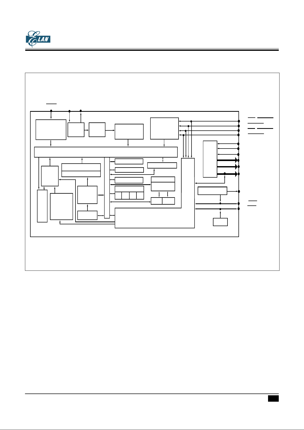
FUNCTION BLOCK DIAGRAMFUNCTION BLOCK DIAGRAM
FUNCTION BLOCK DIAGRAMFUNCTION BLOCK DIAGRAM
FUNCTION BLOCK DIAGRAM
Interrupt
Control
Time
Base
12-bit
timer
counter
(TA,TB)
System Control
Instruction Decoder
Instruction Register
ROM
PC
Data Bus
Reset
Control
Frequency
doubler
Timing
Generator
Sleep Mode
Control
Data pointer
ACC
ALU
Flag
ZCS G
Stack pointer
Stack
RAM
HR
LR
I/O Control
P0.0(INT1)/WAKEUP0
P0.1/WAKEUP1
P0.2(INT0)/WAKEUP2
P0.3/WAKEUP3
RESET
Clock
Generator
XIN
XOUT
LCD
driver
Tone generator
WDT
VA
VB
VEE
COM0~COM2
SEG0~SEG12
P4.0/TONE
P4.1/WDT
TONE
P4,P5,P6,P7/SEG(26..13)
Page 4
4
* This specification are subject to be changed without notice.
12.17.2001
EM73P361AEM73P361A
EM73P361AEM73P361A
EM73P361A
4-BIT MICRO-CONTROLLER FOR LCD PRODUCT4-BIT MICRO-CONTROLLER FOR LCD PRODUCT
4-BIT MICRO-CONTROLLER FOR LCD PRODUCT4-BIT MICRO-CONTROLLER FOR LCD PRODUCT
4-BIT MICRO-CONTROLLER FOR LCD PRODUCT
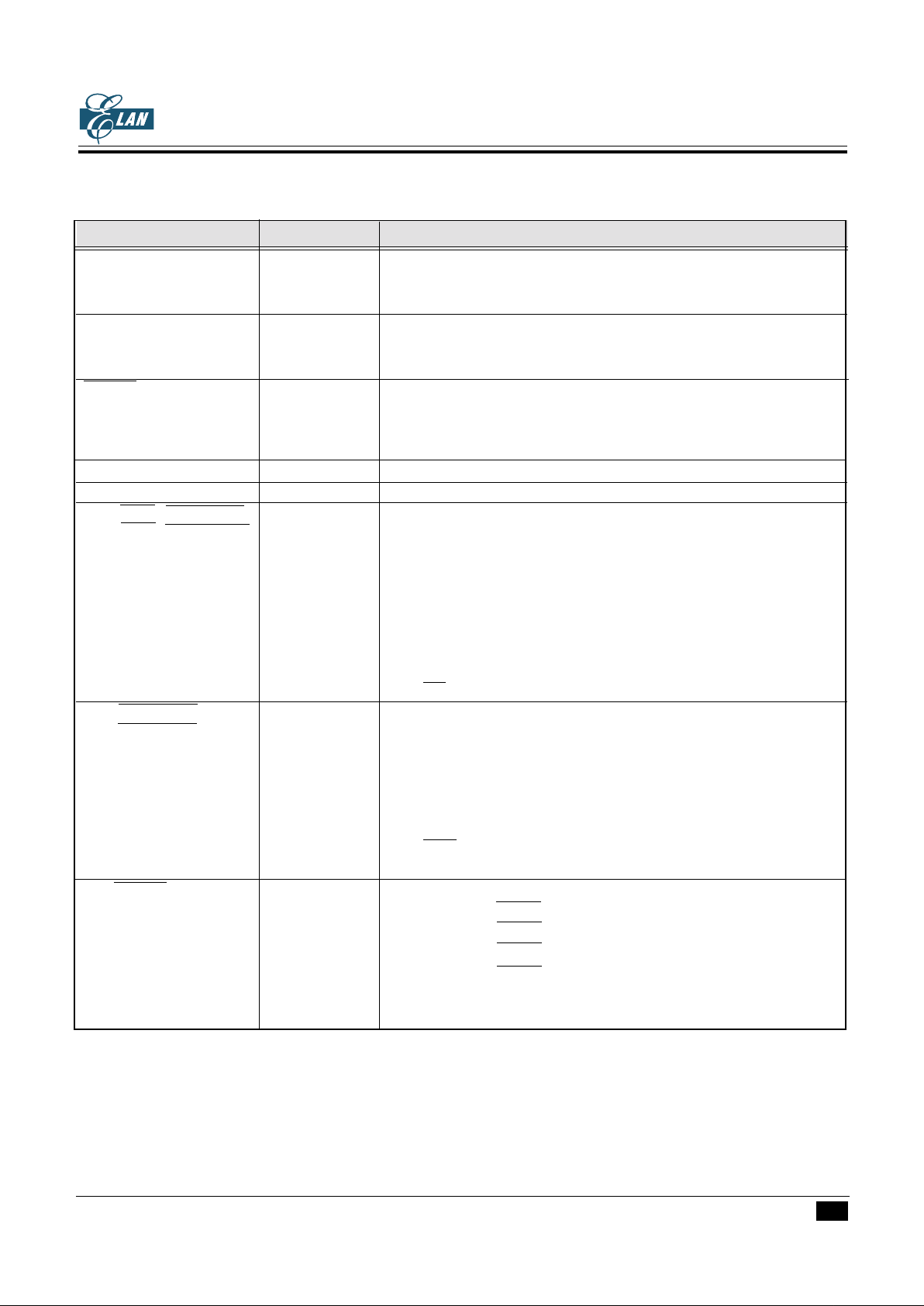
SymbolSymbol
SymbolSymbol
Symbol
Pin-typePin-type
Pin-typePin-type
Pin-type
FunctionFunction
FunctionFunction
Function
V
DD
Power supply (+)
In programming OTP mode:
Power supply (+)
VSS Power supply (-)
In programming OTP mode:
Power supply (-)
RESET RESET-A System reset input signal, low active
Internal pull-up
In programming OTP mode:
Reset input pin, low active
XIN OSC-A/OSC-F Crystal/external resistor or external clock source connecting pin
XOUT OSC-A/OSC-F Crystal/external resistor connecting pin
P0.0(INT1)/WAKEUP0, INPUT-J 2-bit input port with external interrupt sources input and Sleep/Hold
P0.2(INT0)/WAKEUP2 releasing function
mask option : wakeup enable, pull-up
wakeup enable, none
wakeup disable, pull-up
wakeup disable, none
wakeup disable, pull-down
In programming OTP mode:
P0.0/ACLK: address counter clock for programming OTP
P0.2/OE: data output enable for programming OTP
P0.1/WAKEUP1, INPUT-H 2-bit input port with Sleep/Hold releasing function
P0.3/WAKEUP3 mask option : wakeup enable, pull-up
wakeup enable, none
wakeup disable, pull-up
wakeup disable, pull-down
wakeup disable, none
In programming OTP mode:
P0.1/PGM: program data to OTP for programming OTP
P0.3/DCLK: data in/out clock signal for programming OTP
P4.0/TONE I/O-O 1-bit bidirection I/O pin or inverse tone generator output
mask option : TONE enable, push-pull, high current PMOS
TONE disable, open-drain
TONE disable, push-pull, high current PMOS
TONE disable, push-pull, low current PMOS
In programming OTP mode:
P4.0/DIN : data input for programming OTP
PIN DESCRIPTIONSPIN DESCRIPTIONS
PIN DESCRIPTIONSPIN DESCRIPTIONS
PIN DESCRIPTIONS
Page 5
5
* This specification are subject to be changed without notice.
12.17.2001
EM73P361AEM73P361A
EM73P361AEM73P361A
EM73P361A
4-BIT MICRO-CONTROLLER FOR LCD PRODUCT4-BIT MICRO-CONTROLLER FOR LCD PRODUCT
4-BIT MICRO-CONTROLLER FOR LCD PRODUCT4-BIT MICRO-CONTROLLER FOR LCD PRODUCT
4-BIT MICRO-CONTROLLER FOR LCD PRODUCT
FUNCTION DESCRIPTIONSFUNCTION DESCRIPTIONS
FUNCTION DESCRIPTIONSFUNCTION DESCRIPTIONS
FUNCTION DESCRIPTIONS
PROGRAM ROM ( 3K X 8 bits )PROGRAM ROM ( 3K X 8 bits )
PROGRAM ROM ( 3K X 8 bits )PROGRAM ROM ( 3K X 8 bits )
PROGRAM ROM ( 3K X 8 bits )
3 K x 8 bits program ROM contains user's program and some fixed data .
The basic structure of program ROM can be divided into 4 parts.
1. Address 000h: Reset start address.
2. Address 002h - 00Ch: 4 kinds of interrupt service routine entry addresses .
3. Address 00Eh-086h : SCALL subroutine entry address, only available at 00Eh,016h,01Eh,026h, 02Eh,
036h, 03Eh, 046h, 04Eh, 056h, 05Eh, 066h, 06Eh, 076h ,07Eh, 086h .
4. Address 000h - 7FFh : LCALL subroutine entry address
5. Address 000h - BFFh : Except used as above function, the other region can be used as user's program region.
address 3072 x 8 bits
000h Reset start address
002h INT0 ; External interrupt service toutine entry address
004h
006h TRGA; Timer/counter A interrupt service routine entry address
008h TRGB; Timer/counter B interrupt service routine entry address
00Ah TBI; Time base interrupt service routine entry address
00Ch INT1; External interrupt service routine entry address
00Eh
086h
BFFh
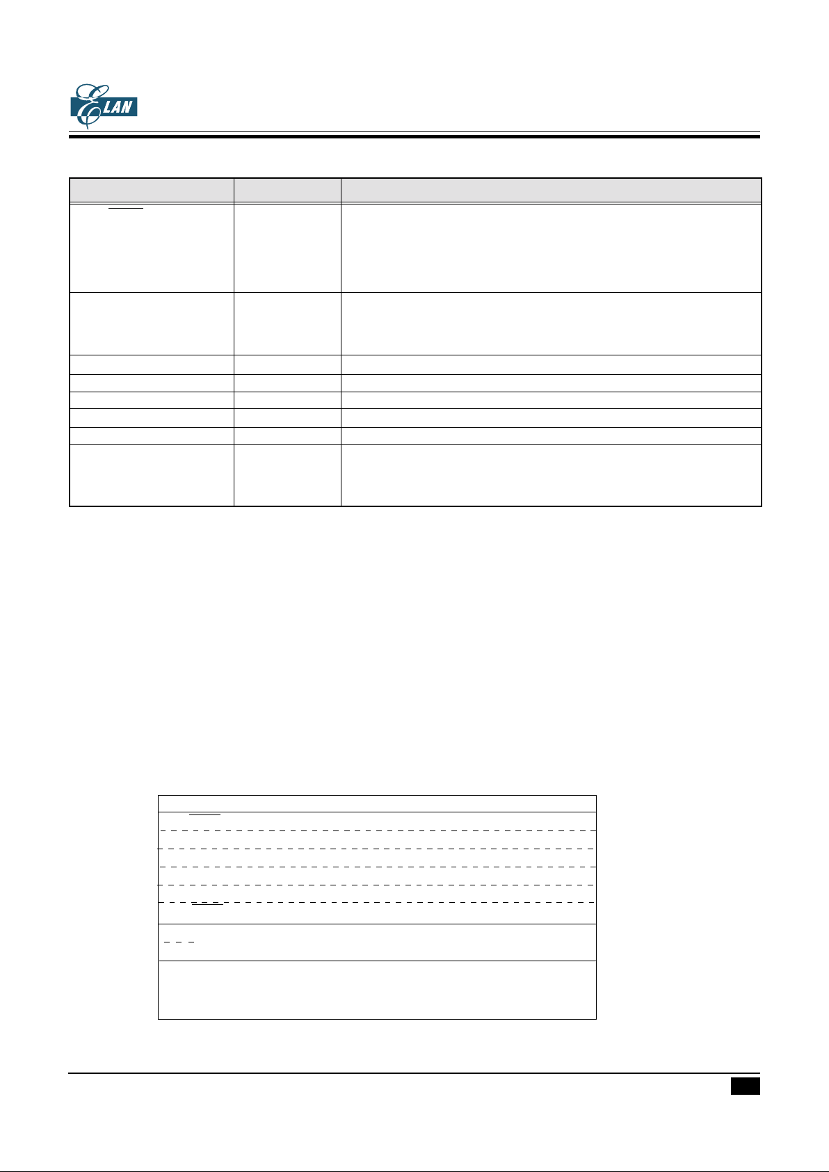
SymbolSymbol
SymbolSymbol
Symbol
Pin-typePin-type
Pin-typePin-type
Pin-type
FunctionFunction
FunctionFunction
Function
P4.1/WDT I/O-D 1-bit bidirection I/O pin with watch-dog-timer output
mask option : open-drain
push-pull
In programming OTP mode:
P4.1/DOUT: data output for programming OTP
P4(2..3)/SEG(26..25) I/O-P 4-bit bidirection I/O ports are shared with LCD segment pins
P5(0..3)/SEG(24..21) mask option : segment enable, open-drain
P6(0..3)/SEG(20..17) segment disable, push-pull
P7(0..3)/SEG(16..13) segment disable, open-drain
TONE Built-in tone generator output
VA, VB, VEE Connect the capacitors for LCD bias voltage
COM0~COM2 LCD common output pins
SEG0~SEG12 LCD segment output pins
TEST Internal pull down
V PP Connect to VDD
In programming OTP mode:
High voltage power source for programming OTP
SCALL, subroutine call entry address
.
.
.
Page 6
6
* This specification are subject to be changed without notice.
12.17.2001
EM73P361AEM73P361A
EM73P361AEM73P361A
EM73P361A
4-BIT MICRO-CONTROLLER FOR LCD PRODUCT4-BIT MICRO-CONTROLLER FOR LCD PRODUCT
4-BIT MICRO-CONTROLLER FOR LCD PRODUCT4-BIT MICRO-CONTROLLER FOR LCD PRODUCT
4-BIT MICRO-CONTROLLER FOR LCD PRODUCT
STACK:
There are 13 - level (maximum) stack for user using for subroutine (including interrupt and CALL). User
can assign any level be the starting stack by giving the level number to stack pointer (SP).
ZERO- PAGE:
From 00h to 0Fh is the location of zero-page. It is used as the pointer in zero -page addressing mode for the
instruction of "STD #k,y; ADD #k,y; CLR y,b; CMP k,y".
PROGRAM EXAMPLE: To wirte immediate data "07h" to address "03h" of RAM and to clear bit 2 of RAM.
STD #07h, 03h ; RAM[03] ← 07h
CLR 0Eh,2 ; RAM[0Eh]2 ← 0
Increment
Address
20h - 2Fh
30h - 33h
Level 0
Level 4
Level 8
Level 12
Level 1
Level 5
Level 9
Level 2
Level 6
Level 10
Level 3
Level 7
Level 11
Increment
00h - 0Fh
10h - 1Fh
Stack Zero-page
DATA RAM ( 52-nibble ) DATA RAM ( 52-nibble )
DATA RAM ( 52-nibble ) DATA RAM ( 52-nibble )
DATA RAM ( 52-nibble )
There is total 52 - nibble data RAM from address 00 to 33h
Data RAM includes 3 parts: zero page region, stacks and data area.
LDAXLDAX
LDAXLDAX
LDAX
Acc Acc
Acc Acc
Acc
←←
←←
←
ROM[DP] ROM[DP]
ROM[DP] ROM[DP]
ROM[DP]
LL
LL
L
LDAXILDAXI
LDAXILDAXI
LDAXI
Acc Acc
Acc Acc
Acc
←←
←←
←
ROM[DP] ROM[DP]
ROM[DP] ROM[DP]
ROM[DP]
HH
HH
H
,DP+1,DP+1
,DP+1,DP+1
,DP+1
DP is a 12-bit data register which can store the program ROM address to be the pointer for the ROM code data.
First, user load ROM address into DP by instruction "STADPL, STADPM, STADPH", then user can get the
lower nibble of ROM code data by instruction "LDAX" and higher nibble by instruction "LDAXI".
PROGRAM EXAMPLE: Read out the ROM code of address 777h by table-look-up instruction.
LDIA #07h;
STADPL ; [DP]L ← 07h
STADPM ; [DP]M ← 07h
STADPH ; [DP]H ← 07h, Load DP=777h
:
LDL #00h;
LDH #03h;
LDAX ; ACC ← 6h
STAMI ; RAM[30] ← 6h
LDAXI ; ACC ← 5h
STAM ; RAM[31] ← 5h
;
ORG 777h
DATA 56h;
:
Table-look-up instruction is depended on the Data Pointer ( DP ) to indicate to ROM address, then to get the
ROM code data.
User's program and fixed data are stored in the program ROM. User's program is according the PC value
to send next executed instruction code. Fixed data can be read out by table-look-up instruction.
Page 7
7
* This specification are subject to be changed without notice.
12.17.2001
EM73P361AEM73P361A
EM73P361AEM73P361A
EM73P361A
4-BIT MICRO-CONTROLLER FOR LCD PRODUCT4-BIT MICRO-CONTROLLER FOR LCD PRODUCT
4-BIT MICRO-CONTROLLER FOR LCD PRODUCT4-BIT MICRO-CONTROLLER FOR LCD PRODUCT
4-BIT MICRO-CONTROLLER FOR LCD PRODUCT
When user using any instruction of CALL or subroutine, before entry the subroutine, the previous PC address
will be saved into stack until return from those subroutines, the PC value will be restored by the data saved
in stack.
DATA AREA:
Except the special area used by user, the whole RAM can be used as data area for storing and loading general
data.
ADDRESSING MODE
(1) Indirect addressing mode:
Indirect addressing mode indicates the RAM address by specified HL register.
For example:
LDAM ; Acc ← RAM[HL]
STAM ; RAM[HL] ← Acc
(2) Direct addressing mode:
Direct addressing mode indicates the RAM address by immediate data.
For example: LDA x ; Acc← RAM[x]
STA x ; RAM[x] ← Acc
(3) Zero-page addressing mode
For zero-page region, user can using direct addressing to write or do any arithematic, comparsion or bit
manupulated operation directly.
For example: STD #k,y ; RAM[y] ← #k
ADD #k,y; RAM[y] ← RAM[y] + #k
PROGRAM COUNTER (3K ROM)PROGRAM COUNTER (3K ROM)
PROGRAM COUNTER (3K ROM)PROGRAM COUNTER (3K ROM)
PROGRAM COUNTER (3K ROM)
Program counter ( PC ) is composed by a 12-bit counter, which indicates the next executed address for the
instruction of program ROM.
For a 3K - byte size ROM, PC can indicate address form 000h - BFFh, for BRANCH and CALL instrcutions,
PC is changed by instruction indicating.
(1) Branch instruction:(1) Branch instruction:
(1) Branch instruction:(1) Branch instruction:
(1) Branch instruction:
SBR aSBR a
SBR aSBR a
SBR a
Object code: 00aa aaaa
Condition: SF=1; PC ← PC
11-6.a
( branch condition satisified )
PC Hold original PC value+1 aaaaaa
SF=0; PC← PC +1( branch condition not satisified)
PC Original PC value + 1
LBR aLBR a
LBR aLBR a
LBR a
Object code: 1100 aaaa aaaa aaaa
Condition: SF=1; PC ← a ( branch condition satisified)
PCaaaaaaaaaaaa
Page 8
8
* This specification are subject to be changed without notice.
12.17.2001
EM73P361AEM73P361A
EM73P361AEM73P361A
EM73P361A
4-BIT MICRO-CONTROLLER FOR LCD PRODUCT4-BIT MICRO-CONTROLLER FOR LCD PRODUCT
4-BIT MICRO-CONTROLLER FOR LCD PRODUCT4-BIT MICRO-CONTROLLER FOR LCD PRODUCT
4-BIT MICRO-CONTROLLER FOR LCD PRODUCT
SF=0 ; PC ← PC + 2 ( branch condition not satisified )
PC Original PC value + 2
(2) Subroutine instruction:(2) Subroutine instruction:
(2) Subroutine instruction:(2) Subroutine instruction:
(2) Subroutine instruction:
SCALL aSCALL a
SCALL aSCALL a
SCALL a
Object code: 1110 nnnn
Condition : PC ← a ; a=8n+6 ; n=1..15 ; a=86h, n=0
LCALL aLCALL a
LCALL aLCALL a
LCALL a
Object code: 0100 0aaa aaaa aaaa
Condition: PC ← a
PC0aaaaaaaaaaa
RETRET
RETRET
RET
Object code: 0100 1111
Condition: PC ← STACK[SP]; SP + 1
PC The return address stored in stack
RT IRT I
RT IRT I
RT I
Object code: 0100 1101
Condition : FLAG. PC ← STACK[SP]; EI ← 1; SP + 1
PC The return address stored in stack
(3) Interrupt acceptance operation:(3) Interrupt acceptance operation:
(3) Interrupt acceptance operation:(3) Interrupt acceptance operation:
(3) Interrupt acceptance operation:
When an interrupt is accepted, the original PC is pushed into stack and interrupt vector will be loaded into
PC,The interrupt vectors are as following:
INT0 INT0
INT0 INT0
INT0 (External interrupt from P0.2)
PC000000000010
TRGATRGA
TRGATRGA
TRGA (Timer A overflow interrupt)
PC000000000110
TRGBTRGB
TRGBTRGB
TRGB (Time B overflow interrupt)
PC000000001000
TBITBI
TBITBI
TBI (Time base interrupt)
PC000000001010
PC 0 0 0 0 a a a a a a a a
Page 9
9
* This specification are subject to be changed without notice.
12.17.2001
EM73P361AEM73P361A
EM73P361AEM73P361A
EM73P361A
4-BIT MICRO-CONTROLLER FOR LCD PRODUCT4-BIT MICRO-CONTROLLER FOR LCD PRODUCT
4-BIT MICRO-CONTROLLER FOR LCD PRODUCT4-BIT MICRO-CONTROLLER FOR LCD PRODUCT
4-BIT MICRO-CONTROLLER FOR LCD PRODUCT
INT1 INT1
INT1 INT1
INT1 (External interrupt from P0.0)
PC000000001100
(4) Reset operation:(4) Reset operation:
(4) Reset operation:(4) Reset operation:
(4) Reset operation:
PC000000000000
(5) Other operations:(5) Other operations:
(5) Other operations:(5) Other operations:
(5) Other operations:
For 1-byte instruction execution: PC + 1
For 2-byte instruction execution: PC + 2
There are four kinds of flag, CF ( Carry flag ), ZF ( Zero flag ), SF ( Status flag ) and GF ( General flag ),
these 4 1-bit flags are affected by the arithematic, logic and comparative .... operation .
All flags will be put into stack when an interrupt subroutine is served, and the flags will be restored after
RTI instruction executed .
(1) Carry Flag ( CF )
The carry flag is affected by following operation:
a. Addition : CF as a carry out indicator, when the addition operation has a carry-out, CF will be "1",
in another word, if the operation has no carry-out, CF will be "0".
b. Subtraction : CF as a borrow-in indicator, when the subtraction operation must has a borrow, in the CF
will be "0", in another word, if no borrow-in, CF will be "1".
c. Comparision: CF is as a borrow-in indicator for Comparision operation as the same as subtraction
operation.
d. Rotation: CF shifts into the empty bit of accumulator for the rotation and holds the shift out data after
rotation.
e. CF test instruction : For TFCFC instruction, the content of CF sends into SF then clear itself "0".
For TTSFC instruction, the content of CF sends into SF then set itself "1".
(2) Zero Flag ( ZF )
ZF is affected by the result of ALU, if the ALU operation generate a "0" result, the ZF will be "1",
otherwise, the ZF will be "0".
(3) Status Flag ( SF )
The SF is affected by instruction operation and system status .
ACCUMULATORACCUMULATOR
ACCUMULATORACCUMULATOR
ACCUMULATOR
Accumulator is a 4-bit data register for temporary data . For the arithematic, logic and comparative opertion
.., ACC plays a role which holds the source data and result .
FLAGSFLAGS
FLAGSFLAGS
FLAGS
Page 10
10
* This specification are subject to be changed without notice.
12.17.2001
EM73P361AEM73P361A
EM73P361AEM73P361A
EM73P361A
4-BIT MICRO-CONTROLLER FOR LCD PRODUCT4-BIT MICRO-CONTROLLER FOR LCD PRODUCT
4-BIT MICRO-CONTROLLER FOR LCD PRODUCT4-BIT MICRO-CONTROLLER FOR LCD PRODUCT
4-BIT MICRO-CONTROLLER FOR LCD PRODUCT
ALUALU
ALUALU
ALU
The arithematic operation of 4 - bit data is performed in ALU unit . There are 2 flags can be affected by
the result of ALU operation, ZF and SF . The operation of ALU can be affected by CF only .
ALU STRUCTUREALU STRUCTURE
ALU STRUCTUREALU STRUCTURE
ALU STRUCTURE
ALU supported user arithematic operation function, including : addition, subtraction and rotaion.
ALU FUNCTIONALU FUNCTION
ALU FUNCTIONALU FUNCTION
ALU FUNCTION
(1) Addition:
For instruction ADDAM, ADCAM, ADDM #k, ADD #k,y .... ALU supports addition function.
The addition operation can affect CF and ZF. For addition operation, if the result is "0", ZF will be "1",
otherwise, not equal "0", ZF will be "0", When the addition operation has a carry-out. CF will be "1",
otherwise, CF will be "0".
EXAMPLE:
Operation Carry Zero
3+4=7 0 0
7+F=6 1 0
0+0=0 0 1
8+8=0 1 1
(2) Subtraction:
For instruction SUBM #k, SUBA #k, SBCAM, DECM... ALU supports user subtraction function . The
subtraction operation can affect CF and ZF, For subtraction operation, if the result is negative, CF will
GF is a one bit general purpose register which can be set, clear, test by instruction SGF, CGF and TGS.
PROGRAM EXAMPLE:
Check following arithematic operation for CF, ZF, SF
CF ZF SF
LDIA #00h; - 1 1
LDIA #03h; - 0 1
ADDA #05h; - 0 1
ADDA #0Dh; - 0 0
ADDA #0Eh; - 0 0
a. SF is initiated to "1" for reset condition .
b. Branch instruction is decided by SF, when SF=1, branch condition will be satisified, otherwise,
branch condition will not be satisified by SF = 0 .
(4) General Flag ( GF )
ZF CF SF GF
ALU
DATA BUS
Page 11
11
* This specification are subject to be changed without notice.
12.17.2001
EM73P361AEM73P361A
EM73P361AEM73P361A
EM73P361A
4-BIT MICRO-CONTROLLER FOR LCD PRODUCT4-BIT MICRO-CONTROLLER FOR LCD PRODUCT
4-BIT MICRO-CONTROLLER FOR LCD PRODUCT4-BIT MICRO-CONTROLLER FOR LCD PRODUCT
4-BIT MICRO-CONTROLLER FOR LCD PRODUCT
ACC
CF
MSB LSB
3 2 1 0
H REGISTER
3 2 1 0
L REGISTER
ACC
CF
MSB LSB
(3) Rotation:
There are two kinds of rotation operation, one is rotation left, the other is rotation right.
RLCA instruction rotates Acc value to left, shift the CF value into the LSB bit of Acc and the shift out data
will be hold in CF.
RRCA instruction operation rotates Acc value to right, shift the CF value into the MSB bit of Acc and the
shift out data will be hold in CF.
PROGRAM EXAMPLE: To rotate Acc right and shift a "1" into the MSB bit of Acc .
TTCFS; CF ← 1
RRCA; rotate Acc right and shift CF=1 into MSB.
HL REGISTERHL REGISTER
HL REGISTERHL REGISTER
HL REGISTER
HL register are two 4-bit registers, they are used as a pair of pointer for the address of RAM memory and also
2 independent temporary 4-bit data registers. For some instruction, L register can be a pointer to indicate the
pin number ( Port4, Port6, Port7 ) .
HL REGISTER STRUCTUREHL REGISTER STRUCTURE
HL REGISTER STRUCTUREHL REGISTER STRUCTURE
HL REGISTER STRUCTURE
HL REGISTER FUNCTIONHL REGISTER FUNCTION
HL REGISTER FUNCTIONHL REGISTER FUNCTION
HL REGISTER FUNCTION
(1)For instruction : LDL #k, LDH #k, THA, THL, INCL, DECL, EXAL, EXAH, HL register used as a
temporary register .
PROGRAM EXAMPLE: Load immediate data "5h" into L register, "Dh" into H register.
LDL #05h;
LDH #0Dh;
(2) For instruction LDAM, STAM, STAMI .., HL register used as a pointer for the address of RAM memory.
EXAMPLE:
Operation Carry Zero
8-4=4 1 0
7-F= -8(1000) 0 0
9-9=0 1 1
be "0", it means a borrow out, otherwise, if the result is positive, CF will be "1". For ZF, if the result
of subtraction operation is "0", the ZF will be "1", otherwise, ZF will be "1".
Page 12

12
* This specification are subject to be changed without notice.
12.17.2001
EM73P361AEM73P361A
EM73P361AEM73P361A
EM73P361A
4-BIT MICRO-CONTROLLER FOR LCD PRODUCT4-BIT MICRO-CONTROLLER FOR LCD PRODUCT
4-BIT MICRO-CONTROLLER FOR LCD PRODUCT4-BIT MICRO-CONTROLLER FOR LCD PRODUCT
4-BIT MICRO-CONTROLLER FOR LCD PRODUCT
PROGRAM EXAMPLE: Store immediate data #Ah into RAM of address 35h.
LDL #5h;
LDH #3h;
STDMI #0Ah; RAM[35] ← Ah
(3) For instruction : SELP, CLPL, TFPL, L regieter be a pointer to indicate the bit of I/O port.
When LR = 0 - 1, indicate P4.0 - P4.1.
PROGRAM EXAMPLE: To set bit 1 of Port4 to "1"
LDL #01h;
SEPL ; P4.1 ← 1
STACK POINTER (SP)STACK POINTER (SP)
STACK POINTER (SP)STACK POINTER (SP)
STACK POINTER (SP)
Stack pointer is a 4-bit register which stores the present stack level number.
Before using stack, user must set the SP value first, CPU will not initiate the SP value after reset condition
. When a new subroutine is accepted, the SP will be decreased one automatically, in another word, if
returning from a subroutine, the SP will be increased one .
The data transfer between ACC and SP is by instruction of "LDASP" and "STASP".
DATA POINTER (DP)DATA POINTER (DP)
DATA POINTER (DP)DATA POINTER (DP)
DATA POINTER (DP)
Data pointer is a 12-bit register which stores the address of ROM can indicate the ROM code data
specified by user (refer to data ROM).
CLOCK AND TIMING GENERATORCLOCK AND TIMING GENERATOR
CLOCK AND TIMING GENERATORCLOCK AND TIMING GENERATOR
CLOCK AND TIMING GENERATOR
The clock generator is supported by a single clock system, the clock source comes from crystal (resonator)
or RC oscillation, the working frequency range is 32 KHz to 100 KHz depending on the working voltage.
CLOCK AND TIMING GENERATOR STRUCTURECLOCK AND TIMING GENERATOR STRUCTURE
CLOCK AND TIMING GENERATOR STRUCTURECLOCK AND TIMING GENERATOR STRUCTURE
CLOCK AND TIMING GENERATOR STRUCTURE
The clock generator connects outside compoments ( crystal or resonator by XIN and XOUT pin for crystal
osc type, capacitor for RC osc type, these two type is decided by mask option) the clock generator generates
a basic system clock "fc".
When CPU sleeping, the clock generator will be stoped until the sleep condition released.
The system clock control generates 4 basic phase signals ( S1, S2, S3, S4 ) and system clock .
sleep
XIN/CLK
XOUT
clock generator System clock control
fc
System clock
S1 S2 S3 S4
Mask option
Mask option for choose Crystal or RC oscillation
XIN
Page 13

13
* This specification are subject to be changed without notice.
12.17.2001
EM73P361AEM73P361A
EM73P361AEM73P361A
EM73P361A
4-BIT MICRO-CONTROLLER FOR LCD PRODUCT4-BIT MICRO-CONTROLLER FOR LCD PRODUCT
4-BIT MICRO-CONTROLLER FOR LCD PRODUCT4-BIT MICRO-CONTROLLER FOR LCD PRODUCT
4-BIT MICRO-CONTROLLER FOR LCD PRODUCT
CLOCK AND TIMING GENERATOR FUNCTIONCLOCK AND TIMING GENERATOR FUNCTION
CLOCK AND TIMING GENERATOR FUNCTIONCLOCK AND TIMING GENERATOR FUNCTION
CLOCK AND TIMING GENERATOR FUNCTION
The frequency of fc is the oscillation frequency for XIN, XOUT by crystal ( resonator) or by RC osc.
When CPU sleeps, the XOUT pin will be in "high" state .
The instruction cycle equal 4 basic clock fc.
1 instructure cycle = 4 / fc
TIMING GENERATOR AND TIME BASETIMING GENERATOR AND TIME BASE
TIMING GENERATOR AND TIME BASETIMING GENERATOR AND TIME BASE
TIMING GENERATOR AND TIME BASE
The timing generator produces the system clock from basic clock pulse which can be normal mode or slow
mode clock.
1 instruction cycle = 4 basic clock pulses
There are 22 stages time base .
When working in the single clock mode, the timebase clock source is come from fc.
Time base provides basic frequency for following function:
1. TBI (time base interrupt) .
2. Timer/counter, internal clock source.
3. Warm-up time for sleep - mode releasing.
TIME BASE INTERRUPT (TBI )TIME BASE INTERRUPT (TBI )
TIME BASE INTERRUPT (TBI )TIME BASE INTERRUPT (TBI )
TIME BASE INTERRUPT (TBI )
The time base can be used to generate a fixed frequency interrupt . There are 8 kinds of frequencies can be
selected by setting "P25"
Single clock mode
P25 3 2 1 0
( initial value 0000 )
0 0 x x: Interrupt disable
0 1 0 0: Interrupt frequency XIN / 29 Hz
0 1 0 1: Interrupt frequency XIN / 2
10
Hz
0 1 1 0: Interrupt frequency XIN / 2
12
Hz
0 1 1 1: Interrupt frequency XIN / 2
13
Hz
1 1 0 0: Interrupt frequency XIN / 2
14
Hz
1 1 0 1: Interrupt frequency XIN / 2
15
Hz
1 1 1 0: Interrupt frequency XIN / 2
16
Hz
1 1 1 1: Interrupt frequency XIN / 2
17
Hz
1 0 x x: Reserved
fc
Prescaler
Binary counter
123
0 5 6 7 8 9 10 11 12 134212019 181716 15 14
XIN
XOUT
Crystal connection
XIN
XOUT
Resistor connection
Page 14

14
* This specification are subject to be changed without notice.
12.17.2001
EM73P361AEM73P361A
EM73P361AEM73P361A
EM73P361A
4-BIT MICRO-CONTROLLER FOR LCD PRODUCT4-BIT MICRO-CONTROLLER FOR LCD PRODUCT
4-BIT MICRO-CONTROLLER FOR LCD PRODUCT4-BIT MICRO-CONTROLLER FOR LCD PRODUCT
4-BIT MICRO-CONTROLLER FOR LCD PRODUCT
INTERRUPT CONTROL
TRGA request
TIMER CONTROL
i
nternal clock
P28
12 BIT COUNTER
TMSA IPSA
DATA BUS
TIMER CONTROL
internal clock
P29
12 BIT COUNTER
TMSB IPSB
TRGB request
Port 28
3 2 1 0
TMSA IPSA
Initial state: 0000
TIMER/COUNTER MODE SELECTION
TMSA (B) Function description
0 0 Stop
0 1 Reserved
1 0 Timer mode
1 1 Reserved
Port 29
3 2 1 0
TMSB IPSB
Initial state: 0000
INTERNAL PULSE-RATE SELECTION
IPSA(B) Function description
0 0 XIN/2 Hz
0 1 XIN/2 Hz
1 0 XIN/2 Hz
1 1 XIN/2 Hz
5
7
11
15
TIMER/COUNTER CONTROLTIMER/COUNTER CONTROL
TIMER/COUNTER CONTROLTIMER/COUNTER CONTROL
TIMER/COUNTER CONTROL
Timer/counter command port: P28 is the command port for timer/counterA and P29 is for the timer/
counterB.
TIMER / COUNTER ( TIMERA, TIMERB)TIMER / COUNTER ( TIMERA, TIMERB)
TIMER / COUNTER ( TIMERA, TIMERB)TIMER / COUNTER ( TIMERA, TIMERB)
TIMER / COUNTER ( TIMERA, TIMERB)
EM73P361A only can support timer function for timerA and timerB independently.
For timerA, the counter data is saved in timer register TAH, TAM, TAL, which user can set counter initial
value and read the counter value by instruction "LDATAH(M,L), STATAH(M,L)" and timerB register is
TBH, TBM, TBL and W/R instruction "LDATBH (M,L), STATBH (M,L)".
The basic structure of timer/counter is composed by two same structure counter, these two counters can be
set initial value and send counter value to timer register, P28 and P29 are the command ports for timerA
and timer B, user can choose different internal clock rate by setting these two ports. When timer/counter
overflow, it will generate a TRGA(B) interrupt request to interrupt control unit.
Page 15

15
* This specification are subject to be changed without notice.
12.17.2001
EM73P361AEM73P361A
EM73P361AEM73P361A
EM73P361A
4-BIT MICRO-CONTROLLER FOR LCD PRODUCT4-BIT MICRO-CONTROLLER FOR LCD PRODUCT
4-BIT MICRO-CONTROLLER FOR LCD PRODUCT4-BIT MICRO-CONTROLLER FOR LCD PRODUCT
4-BIT MICRO-CONTROLLER FOR LCD PRODUCT
TIMER/COUNTER FUNCTIONTIMER/COUNTER FUNCTION
TIMER/COUNTER FUNCTIONTIMER/COUNTER FUNCTION
TIMER/COUNTER FUNCTION
Each timer/counter can execute the timer function independly.
TIMER MODE
For timer mode ,timer/counter increase one at any rising edge of internal pulse . User can choose 4 kinds
of internal pulse rate by setting IPSB for timerB (IPSA for timerA).
When timer/counter counts overflow, TRGB (TRGA) will be generated to interrupt control unit.
PROGRAM EXAMPLE: To generate TRGA interrupt request after 60 ms with system clock XlN=32K Hz
LDIA #0100B;
EXAE; enable mask 2
EICIL 110111B; internupt latch ← 0, enable EI
LDIA #04H;
LDIA #0CH;
STATAM;
LDIA #0FH;
STATAH;
LDIA #1000B;
OUTA P28; enable timerA with internal pulse rate: XIN/25 Hz
NOTE: The preset value of timer/counter register is calculated as following procedure.
Internal pulse rate: XIN/2
5
; XIN = 32KHz
The time of timer counter count one = 25 /XIN = 32/32K=1ms
The number of internal pulse to get timer overflow = 60 ms/ 1ms = 60 = 03CH
The preset value of timer/counter register = 1000H - 03CH = 0FC4H
INTERRUPT FUNCTIONINTERRUPT FUNCTION
INTERRUPT FUNCTIONINTERRUPT FUNCTION
INTERRUPT FUNCTION
There are 3 internal interrupt sources and 2 external interrupt sources. Multiple interrupts are admitted
according the priority .
TypeType
TypeType
Type
Interrupt sourceInterrupt source
Interrupt sourceInterrupt source
Interrupt source
PriorityPriority
PriorityPriority
Priority
InterruptInterrupt
InterruptInterrupt
Interrupt
InterruptInterrupt
InterruptInterrupt
Interrupt
Program ROMProgram ROM
Program ROMProgram ROM
Program ROM
LatchLatch
LatchLatch
Latch
Enable conditionEnable condition
Enable conditionEnable condition
Enable condition
entry addressentry address
entry addressentry address
entry address
External External interrupt (INT0) 1 IL5 EI=1 002H
Internal Reserved 2 IL4 EI=1, MASK3=1 004H
Internal TimerA overflow interrupt (TRGA) 3 IL3 EI=1, MASK2=1 006H
Internal TimerB overflow interrupt (TRGB) 4 IL2 EI=1, MASK1=1 008H
Internal Time base interrupt(TBI) 5 IL1 00AH
External External interrupt (INT1) 6 IL0 EI=1,MASK0=1 00CH
STATAL;
Internal pulse
TimerB (TimerA )value
n n+1 n+2 n+3 n+4 n+5 n+6
n+7
Page 16

16
* This specification are subject to be changed without notice.
12.17.2001
EM73P361AEM73P361A
EM73P361AEM73P361A
EM73P361A
4-BIT MICRO-CONTROLLER FOR LCD PRODUCT4-BIT MICRO-CONTROLLER FOR LCD PRODUCT
4-BIT MICRO-CONTROLLER FOR LCD PRODUCT4-BIT MICRO-CONTROLLER FOR LCD PRODUCT
4-BIT MICRO-CONTROLLER FOR LCD PRODUCT
INTERRUPT STRUCTUREINTERRUPT STRUCTURE
INTERRUPT STRUCTUREINTERRUPT STRUCTURE
INTERRUPT STRUCTURE
Interrupt controller:
IL0-IL5 : Interrupt latch . Hold all interrupt requests from all interrupt sources. ILr can not be
set by program, but can be reset by program or system reset, so IL only can decide
which interrupt source can be accepted.
MASK0-MASK3 : MASK register can promit or inhibit all interrupt sources.
EI : Enable interrupt Flip-Flop can promit or inhibit all interrupt sources, when inter-
rupt happened, EI is cleared to "0" automatically, after RTI instruction happened,
EI will be set to "1" again .
Priority checker: Check interrupt priority when multiple interrupts happened.
INTERRUPT FUNCTIONINTERRUPT FUNCTION
INTERRUPT FUNCTIONINTERRUPT FUNCTION
INTERRUPT FUNCTION
The procedure of interrupt operation:
1. Push PC and all flags to stack.
2. Set interrupt entry address into PC.
3. Set SF= 1.
4. Clear EI to inhibit other interrupts happened.
5. Clear the IL for which interrupt source has already be accepted.
6. To excute interrupt subroutine from the interrupt entry address.
7. CPU accept RTI, restore PC and flags from stack . Set EI to accept other interrupt requests.
PROGRAM EXAMPLE: To enable interrupt of "TRGA"
LDIA #1100B;
EXAE; set mask register "1100B"
EICIL 111111B ; enable interrupt F.F.
INT1
Reset by system reset and program
i
nstruction
MASK0 MASK1 MASK1 MASK2 MASK3
IL0
Reserved
Reserved
r0
IL1
TBI
r1
IL2
r2
IL3
TRGA
r3
IL4
r4
IL5
INT0
r5
Priority checker
EI Entry address generator
Interrupt request Interrupt entry address
Reset by system reset and program
instruction
Set by program instruction
TRGB
INT1
Page 17

17
* This specification are subject to be changed without notice.
12.17.2001
EM73P361AEM73P361A
EM73P361AEM73P361A
EM73P361A
4-BIT MICRO-CONTROLLER FOR LCD PRODUCT4-BIT MICRO-CONTROLLER FOR LCD PRODUCT
4-BIT MICRO-CONTROLLER FOR LCD PRODUCT4-BIT MICRO-CONTROLLER FOR LCD PRODUCT
4-BIT MICRO-CONTROLLER FOR LCD PRODUCT
POWER SAVING FUNCTION ( Sleep / Hold function )POWER SAVING FUNCTION ( Sleep / Hold function )
POWER SAVING FUNCTION ( Sleep / Hold function )POWER SAVING FUNCTION ( Sleep / Hold function )
POWER SAVING FUNCTION ( Sleep / Hold function )
During sleep and hold condition, CPU holds the system's internal status with a low power consumption, for
the sleep mode, the system clock will be stoped in the sleep condition and system need a warm up time for
the stability of system clock running after wakeup . In the other way, for the hold mode, the system clock
does not stop at all and it does not need a warm-up time any way.
The sleep and hold mode is controlled by Port 16 and released by P0(0..3)/WAKEUP0..3.
Sleep and hold condition:
1. Osc stop ( sleep only ) and CPU internal status held .
2. Internal time base clear to "0".
3. CPU internal memory ,flags, register, I/O held original states.
4. Program counter hold the executed address after sleep release.
Release condition:
1. Osc start to oscillating.(sleep only).
2. Warm-up time passing ( sleep only ).
3. According PC to execute the following program.
There is one kind of sleep/hold release mode .
1. Edge release mode:
Release sleep/hold condition by the falling edge of any one of P0(0..3)/WAKEUP0..3.
Note : There are 4 independent mask options for wakeup function in EM73360. So, the wakeup function
of P0(0..3)/WAKEUP0..3 are enabled or disabled inpendently.
LCD DRIVERLCD DRIVER
LCD DRIVERLCD DRIVER
LCD DRIVER
EM73P361A can directly drive the liquid crystal display (LCD) and has 27 segment, 3 common output pins.
There are total 27 x 3 dots can be display. The VDD, VEE and VSS pins are the bias voltage inputs of the LCD
driver. The VA and VB are used to the voltage double for 3V system. The method of LCD programming is
I/O mapping.
CONTROL OF LCD DRIVERCONTROL OF LCD DRIVER
CONTROL OF LCD DRIVERCONTROL OF LCD DRIVER
CONTROL OF LCD DRIVER
The LCD driver control command register is P27. When LDC is 00, the LCD is disabled. When LDC is 01,
the LCD is blanking,
P16 3 2 1 0
initial value :0000
SWWT Set wake-up warm-up time
2 /XIN
2 /XIN
2 /XIN
Hold mode
SE Enable sleep/hold
0 Reserved
1 Enable sleep / hold rnode
01Wake-up in edge release mode
Reserved
0 0
0 1
1 0
1 1
17
13
15
WM SE SWWT
WM Set wake-up release mode
Page 18

18
* This specification are subject to be changed without notice.
12.17.2001
EM73P361AEM73P361A
EM73P361AEM73P361A
EM73P361A
4-BIT MICRO-CONTROLLER FOR LCD PRODUCT4-BIT MICRO-CONTROLLER FOR LCD PRODUCT
4-BIT MICRO-CONTROLLER FOR LCD PRODUCT4-BIT MICRO-CONTROLLER FOR LCD PRODUCT
4-BIT MICRO-CONTROLLER FOR LCD PRODUCT
the COM pins are inactive and the SEG pins continously output the display data. When LDC is 11, the LCD
driver enables, the power swich is turned on and it cannot be turned off forever except the CPU is reseted or
sleeping. Users must enable the LCD driver by self when the CPU is waked up.
Port27
3 2 1 0 Initial value : 0000
LDC DUTY
LDC LCD display control DUTY Driving method select
0 0 LCD display disable & change duty 0 0 Reserved
0 1 Blanking 0 1 1/3 duty (1/2 bias)
1 0 Reserved 1 0 1/2 duty (1/2 bias)
1 1 LCD display enable 1 1 Static
LCD driving methods
There are four kinds of driving methods can be selected by DUTY (P27.0~P27.1). The driving waveforms of
LCD driver are as below :
C
O
M
2
C
O
M
1
C
O
M
0
SEG0
SEG1
SEG2
:
COM0
COM1
COM2
SEG0
SEG0-COM0
ON
SEG0-COM1
OFF
Frame
Frame
Frame
ON
OFF
1/3 duty (1/2 bias) 1/2duty (1/2 bias) Static
Driving method bit3 bit2 bit1 bit0
1/3 duty - COM2 COM1 COM0
1/2 duty - - COM1 COM0
Static - - - COM0
LCD drive voltage
EM73P361A provides 2 kinds of LCD bias methods, capacitor divider and resistor divider, when the LCD bias
method is capacitor divider,the VA is connected a capacitor to VB and the VEE is connected a capacitor
to VSS. The output of VEE is 1.5V for LCD bias voltage. When the LCD bias method is resistor divider, the
VEE is floating.
LCD Frame frequency : According to the drive method to set the frame frequency.
Driving method Frame frequency (Hz)
1/3 duty 43 x (3/3) = 43
1/2 duty 43 x (3/2) = 64
Static 43
The relation between LCD display data and driving method
Page 19

19
* This specification are subject to be changed without notice.
12.17.2001
EM73P361AEM73P361A
EM73P361AEM73P361A
EM73P361A
4-BIT MICRO-CONTROLLER FOR LCD PRODUCT4-BIT MICRO-CONTROLLER FOR LCD PRODUCT
4-BIT MICRO-CONTROLLER FOR LCD PRODUCT4-BIT MICRO-CONTROLLER FOR LCD PRODUCT
4-BIT MICRO-CONTROLLER FOR LCD PRODUCT
LCD DISPLAY OPERATIONLCD DISPLAY OPERATION
LCD DISPLAY OPERATIONLCD DISPLAY OPERATION
LCD DISPLAY OPERATION
The LCD programming method is I/O mapping and P10~P12 are must be used.
Address register of LCD display buffer
It is a 5-bit register to specify address for LCD display buffer.
Port11 Port10
3 2 1 0 3 2 1 0 Initial value :0000 0000
A4 A3 A2 A1 A0
Data register of LCD display buffer
P12 is a 3-bit data register to read or write LCD display buffer.
Port12
3 2 1 0 Initial value : 0000
D2 D1 D0
TONE GENERATORTONE GENERATOR
TONE GENERATORTONE GENERATOR
TONE GENERATOR
EM73P361A has a built-in tone generator. It is a binary down counter. When the CPU is reseted or sleeping, the
tone generator is disabled and the output (P4.0/TONE) is high.
XIN
Tone
generator
P23, P24
Output
control
P30.0
TONE
TONE
fo
High
Tone generator command register
Port30 3 2 1 0
* * * SM Initial value : 0000
SM Sound generator mode
0 Tone generator disable
1 Tone generator enable
VA
VB
V
EE
V
DD
V
SS
1.5V
0.1F
3V
VA
VB
V
EE
V
DD
V
SS
3V
• Resistor divider• Capacitor divider
Page 20

20
* This specification are subject to be changed without notice.
12.17.2001
EM73P361AEM73P361A
EM73P361AEM73P361A
EM73P361A
4-BIT MICRO-CONTROLLER FOR LCD PRODUCT4-BIT MICRO-CONTROLLER FOR LCD PRODUCT
4-BIT MICRO-CONTROLLER FOR LCD PRODUCT4-BIT MICRO-CONTROLLER FOR LCD PRODUCT
4-BIT MICRO-CONTROLLER FOR LCD PRODUCT
Tone frequency register
The 8-bit tone frequency register is P24 and P23. The tone frequency will be changed when user output the
different data to P23. Thus, the data must be output to P24 before P23 when user want to change the 8-bit
tone frequency (TF).
Port24 Port23
3 2 1 0 3 2 1 0 Initial value : 1111 1111
Higher nibble register Lower nibble register
** f1=XIN/(TF+1), TF=1~255, TF≠0
** Example : XIN=32K Hz, TF=00110001B.
⇒ fo=32K Hz/50=655.36 Hz
WATCH-DOG-TIMER (MASK OPTION)WATCH-DOG-TIMER (MASK OPTION)
WATCH-DOG-TIMER (MASK OPTION)WATCH-DOG-TIMER (MASK OPTION)
WATCH-DOG-TIMER (MASK OPTION)
Watch-dog-timer can help user to detect the malfunction (runaway) of CPU and give system a time up signal every
certain time . User can use the time up signal to give system a reset signal when system is fail. When CPU is reseted
or sleeping, the watch-dog-timer is disabled. Users must enable the watch-dog-timer by self when CPU is waked
up.
The basic structure of watch-dog-timer control is composed by a 4-stage binary counter and a control unit . the
WDT counter counts for a certain time to check the CPU status, if there is no malfunction happened, the counter
will be cleared and counting . Otherwise, if there is a malfunction happened, the WDT control will send a WDT
signal ( low active ) to outside, user can use this signal to reset CPU . The WDT checking period is assign by
P21 ( WDT command port )
P21 is the control port of watchdog timer, and the watchdog timer timeup signal is output by P4.1/WDT, user can
use this timeup signal (active low) to reset CPU and initialize system.
Port 21 3 2 1 0 Initial value :0000
CWC * * WDT
CWC Clear watchdog timer counter
0 Clear counter then return to 1
1 Nothing
WDT Set watchdog timer detect time
0 3 x 213/fc=3 x 213/32 KHz=0.75 sec
1 7 x 213/fc=7 x 213/32K Hz=1.75 sec
P4.1 OUTPUT
DATA LATCH
P4.1
0 1 2 3
c
ounter clear request
WDT CONTROL
system reset
P4.1 OUTPUT DATA
WDT
command PORT
P21
WDT counter
fc/2
R
S
Q
F/F
13
Page 21

21
* This specification are subject to be changed without notice.
12.17.2001
EM73P361AEM73P361A
EM73P361AEM73P361A
EM73P361A
4-BIT MICRO-CONTROLLER FOR LCD PRODUCT4-BIT MICRO-CONTROLLER FOR LCD PRODUCT
4-BIT MICRO-CONTROLLER FOR LCD PRODUCT4-BIT MICRO-CONTROLLER FOR LCD PRODUCT
4-BIT MICRO-CONTROLLER FOR LCD PRODUCT
PROGRAM EXAMPLE
To enable WDT with
3 x 213/fc detection ftime.
LDIA #0000B
OUTA P21; set WDT detection time and clear WDT counter
RESETTING FUNCTIONRESETTING FUNCTION
RESETTING FUNCTIONRESETTING FUNCTION
RESETTING FUNCTION
When CPU in normal working condition and RESET pin holds in low level for three instruction cycles at least,
then CPU begins to initialize the whole internal states, and when RESET pin changes to high level, CPU begins
to work in normal condition.
The CPU internal state during reset condition is as following table :
Hardware condition in RESET state Initial value
Program counter 000h
Status flag 01h
Interrupt enable flip-flop ( EI ) 00h
MASK0 ,1, 2, 3 00h
Interrupt latch ( IL ) 00h
P10, 11, 12, 16, 21, 25, 27, 28, 29, 30 00h
P4, 5, 6, 7, 23, 24 0Fh
XIN Start oscillation
The RESET pin is a hysteresis input pin and it has a internal pull-up resistor.
The simplest RESET circuit is connect RESET pin with a capacitor to VSS and a diode to VDD.
RESET
Page 22

22
* This specification are subject to be changed without notice.
12.17.2001
EM73P361AEM73P361A
EM73P361AEM73P361A
EM73P361A
4-BIT MICRO-CONTROLLER FOR LCD PRODUCT4-BIT MICRO-CONTROLLER FOR LCD PRODUCT
4-BIT MICRO-CONTROLLER FOR LCD PRODUCT4-BIT MICRO-CONTROLLER FOR LCD PRODUCT
4-BIT MICRO-CONTROLLER FOR LCD PRODUCT
EM73P361A I/O PORT DESCRIPTION :EM73P361A I/O PORT DESCRIPTION :
EM73P361A I/O PORT DESCRIPTION :EM73P361A I/O PORT DESCRIPTION :
EM73P361A I/O PORT DESCRIPTION :
PortPort
PortPort
Port
Input functionInput function
Input functionInput function
Input function
Output functionOutput function
Output functionOutput function
Output function
NoteNote
NoteNote
Note
0 E Input port , wakeup function
1-- -2-- -3-- -4 E Input port E Output port, P4.0/TONE,P4.1/WDT, P4(2..3)
/SEG(26..25)
5 E Input port E P5(0..3)/SEG(24..21)
6 E Input port E P6(0..3)/SEG(20..17)
7 E Input port E P7(0..3)/SEG(16..13)
8-- -9-- --
10 -- I Address register of LCD display buffer low nibble
11 -- I Address register of LCD display buffer high nibble
12 -- I Data register of LCD display buffer
13 -- -14 -- -15 -- -16 I Sleep/Hold mode control register
17 -18 -19 -20 -21 I Watch-dog-timer control register
22 -23 I Sound effect frequency register low nibble
24 I Sound effect frequency register high nibble
25 I Timebase control register
26 -27 I LCD control register
28 I Timer/counter A control register
29 I Timer/counter B control register
30 I Sound effect command register
31 --
Page 23

23
* This specification are subject to be changed without notice.
12.17.2001
EM73P361AEM73P361A
EM73P361AEM73P361A
EM73P361A
4-BIT MICRO-CONTROLLER FOR LCD PRODUCT4-BIT MICRO-CONTROLLER FOR LCD PRODUCT
4-BIT MICRO-CONTROLLER FOR LCD PRODUCT4-BIT MICRO-CONTROLLER FOR LCD PRODUCT
4-BIT MICRO-CONTROLLER FOR LCD PRODUCT
ABSOLUTE MAXIMUM RATINGSABSOLUTE MAXIMUM RATINGS
ABSOLUTE MAXIMUM RATINGSABSOLUTE MAXIMUM RATINGS
ABSOLUTE MAXIMUM RATINGS
ItemsItems
ItemsItems
Items
Sym.Sym.
Sym.Sym.
Sym.
RatingsRatings
RatingsRatings
Ratings
ConditionsConditions
ConditionsConditions
Conditions
Supply Voltage V
DD
-0.5V to 6V
Input Voltage V
IN
-0.5V to VDD+0.5V
Output Voltage V
O
-0.5V to VDD+0.5V
Power Dissipation P
D
200mW T
OPR
=50oC
Operating Temperature T
OPR
0oC to 50oC
Storage Temperature T
STG
-55oC to 125oC
RECOMMENDED OPERATING CONDITIONSRECOMMENDED OPERATING CONDITIONS
RECOMMENDED OPERATING CONDITIONSRECOMMENDED OPERATING CONDITIONS
RECOMMENDED OPERATING CONDITIONS
ItemsItems
ItemsItems
Items
Sym.Sym.
Sym.Sym.
Sym.
RatingsRatings
RatingsRatings
Ratings
ConditionsConditions
ConditionsConditions
Conditions
Supply Voltage V
DD
2.4V to 3.6V Fc=32KHz
Input Voltage V
IH
0.9xVDD to V
DD
V
IL
0V to 0.10xV
DD
Page 24

24
* This specification are subject to be changed without notice.
12.17.2001
EM73P361AEM73P361A
EM73P361AEM73P361A
EM73P361A
4-BIT MICRO-CONTROLLER FOR LCD PRODUCT4-BIT MICRO-CONTROLLER FOR LCD PRODUCT
4-BIT MICRO-CONTROLLER FOR LCD PRODUCT4-BIT MICRO-CONTROLLER FOR LCD PRODUCT
4-BIT MICRO-CONTROLLER FOR LCD PRODUCT
DC ELECTRICAL CHARACTERISTICSDC ELECTRICAL CHARACTERISTICS
DC ELECTRICAL CHARACTERISTICSDC ELECTRICAL CHARACTERISTICS
DC ELECTRICAL CHARACTERISTICS (VDD=3.0±0.3V, VSS=0V, T
OPR
=25oC)
ParametersParameters
ParametersParameters
Parameters
Sym.Sym.
Sym.Sym.
Sym.
Min.Min.
Min.Min.
Min.
Typ.Typ.
Typ.Typ.
Typ.
Max.Max.
Max.Max.
Max.
UnitUnit
UnitUnit
Unit
ConditionsConditions
ConditionsConditions
Conditions
Supply current I
DD
-1020µAV
DD
=3.3V, Cap. divider, no load, no LVR,
Fc=32KHz
-3060µAV
DD
=3.3V, Res. divider, no load, no LVR,
Fc=32KHz
-5085µAV
DD
=3.3V, no load, with LVR, Fc=32KHz
-58µAV
DD
=3.3V, Hold mode, no LVR
- 0.1 1 µA V
DD
=3.3V, sleep mode, no LVR
Hysteresis voltage V
HYS+
0.50V
DD
- 0.75V
DD
V RESET, P0
V
HYS-
0.20V
DD
- 0.40V
DD
V
Input current I
IH
- 20 30 µA Port0, Pull-down, VIH=V
DD
-30 -20 - µA Port0, Pull-up, VIH=V
SS
- - 1 µA Port0, None
I
IL
- -320 -500 µA Push-pull , V
DD
=3.3V, VIL=0.4V, except P4.0, TONE
Output voltage V
OH
2.4 - - V Push-pull, P4.0(high current PMOS), TONE,
V
DD
=2.7V,IOH=-1mA
2.0 - - V Push-pull, P4.0(low current PMOS),
V
DD
=2.7V, IOH=-60µA
V
OL
- - 0.3 V VDD=2.7V, IOL=1mA
Leakage current I
LO
- - 1 µA Open-drain.VDD=3.3V, VO=3.3V
Input resistor R
IN
30 70 110 KΩ RESET
LCD bias voltage V
EE
1
/2VDD-0.11/2V
DD
1
/2VDD+0.1 V Voltage halfer
COM, SEG pins V
01
VDD-0.1 V
DD
- VI
01
=-5µA, Cap. divider
output current V
02
VEE-0.1 V
EE
VEE+0.1 VI
02
=±5µA, Cap. divider
V
03
-VSSVSS+0.1 VI
03
=5µA, Cap. divider
Frequency stability - 20 - % Fc=32KHz, RC osc, R=750KΩ,
[F(3.0V)-F(2.7V)]/F(3.0V)
Frequency variation - 20 - % Fc=32KHz, V
DD
=3.0V,RC osc, R=750KΩ,
[F(typical)-F(worse case)]/F(typical)
LVR reset voltage V
LVR
- 2.2 - V
LVR reset release V
RLVR
- 2.4 - V
voltage
Page 25

25
* This specification are subject to be changed without notice.
12.17.2001
EM73P361AEM73P361A
EM73P361AEM73P361A
EM73P361A
4-BIT MICRO-CONTROLLER FOR LCD PRODUCT4-BIT MICRO-CONTROLLER FOR LCD PRODUCT
4-BIT MICRO-CONTROLLER FOR LCD PRODUCT4-BIT MICRO-CONTROLLER FOR LCD PRODUCT
4-BIT MICRO-CONTROLLER FOR LCD PRODUCT
RESET PIN TYPERESET PIN TYPE
RESET PIN TYPERESET PIN TYPE
RESET PIN TYPE
TYPE RESET-A
RESET
mask option
XIN
XOUT
Crystal
Osc.
XIN
XOUT
RC Osc.
(inverter)
: mask option
WAKEUP function
mask option
: mask option
input data
special function
control input
WAKEUP function
mask option
INPUT PIN TYPEINPUT PIN TYPE
INPUT PIN TYPEINPUT PIN TYPE
INPUT PIN TYPE
TYPE INPUT-H TYPE INPUT-J
OSCILLATION PIN TYPEOSCILLATION PIN TYPE
OSCILLATION PIN TYPEOSCILLATION PIN TYPE
OSCILLATION PIN TYPE
TYPE OSC-A TYPE OSC-F
Page 26

26
* This specification are subject to be changed without notice.
12.17.2001
EM73P361AEM73P361A
EM73P361AEM73P361A
EM73P361A
4-BIT MICRO-CONTROLLER FOR LCD PRODUCT4-BIT MICRO-CONTROLLER FOR LCD PRODUCT
4-BIT MICRO-CONTROLLER FOR LCD PRODUCT4-BIT MICRO-CONTROLLER FOR LCD PRODUCT
4-BIT MICRO-CONTROLLER FOR LCD PRODUCT
I/O PIN TYPEI/O PIN TYPE
I/O PIN TYPEI/O PIN TYPE
I/O PIN TYPE
TYPE I/O TYPE I/O-D
Input
data
Output
data
path B
MUX
path A
TYPE I/O
Output
data
latch
mask option
: mask option
: mask option
Output
data
latch
TYPE I/O
Input
data
Output
data
Special function output
path B
path A
: mask option
Output
data
latch
TYPE I/O
Input
data
Output
data
Special function
output
path B
path A
special function
control output
TYPE I/O-N TYPE I/O-O
Path A : For set and clear bit of port instructions, data goes through path A from output data latch to CPU.
Path B : For input and test instructions, data from output pin go through path B to CPU and the output data latch
will be set to high.
TYPE I/O-P
Page 27

27
* This specification are subject to be changed without notice.
12.17.2001
EM73P361AEM73P361A
EM73P361AEM73P361A
EM73P361A
4-BIT MICRO-CONTROLLER FOR LCD PRODUCT4-BIT MICRO-CONTROLLER FOR LCD PRODUCT
4-BIT MICRO-CONTROLLER FOR LCD PRODUCT4-BIT MICRO-CONTROLLER FOR LCD PRODUCT
4-BIT MICRO-CONTROLLER FOR LCD PRODUCT
APPLICATION CIRCUITAPPLICATION CIRCUIT
APPLICATION CIRCUITAPPLICATION CIRCUIT
APPLICATION CIRCUIT
P0.0
P0.1
P0.2
TONE
P4.0/TONE
RESET
VSS
VA
VB
VEE
XOUT
XIN
20P
32.768KHz
X'tal osc type
0.1µF
0.1µF
SEG0~
SEG12
COM0~
COM2
LCD PANNEL
VBA T
VBA T
VDD
EM73P361A
Buzzer
RESET
3V
20P
XOUT
XIN
RC osc type
Capacitor
driver
VEE
Resistor driver
0.1µF
Page 28

28
* This specification are subject to be changed without notice.
12.17.2001
EM73P361AEM73P361A
EM73P361AEM73P361A
EM73P361A
4-BIT MICRO-CONTROLLER FOR LCD PRODUCT4-BIT MICRO-CONTROLLER FOR LCD PRODUCT
4-BIT MICRO-CONTROLLER FOR LCD PRODUCT4-BIT MICRO-CONTROLLER FOR LCD PRODUCT
4-BIT MICRO-CONTROLLER FOR LCD PRODUCT
PAD DIAGRAMPAD DIAGRAM
PAD DIAGRAMPAD DIAGRAM
PAD DIAGRAM
91
93
95 949697
10
11
12
13
14
15
16
17
18
61
37 38 39 40 41 42 43 44 45 46
62
63
64
65
66
67
68
69
70
71
72
73
74
85
88 868789
90
SEG8
SEG7
SEG6
SEG5
SEG4
SEG3
P7.2
P7.1
P7.3
SEG12
SEG11
SEG10
SEG9
P0.1
P0.0
RESET
VDD
VSS
XIN
P4.1
P4.0
TONE
P0.3
P0.2
P7.0
P6.2
P6.1
P6.0
P5.3
P5.2
P5.1
P4.3
P5.0
P4.2
P6.3
COM2
SEG2
SEG1
SEG0
COM1
COM0
V
EE
VB
VA
(0,0)
Y
X
EM73P361A
92
TEST
ELAN
19
XOUT
VPP
Page 29

29
* This specification are subject to be changed without notice.
12.17.2001
EM73P361AEM73P361A
EM73P361AEM73P361A
EM73P361A
4-BIT MICRO-CONTROLLER FOR LCD PRODUCT4-BIT MICRO-CONTROLLER FOR LCD PRODUCT
4-BIT MICRO-CONTROLLER FOR LCD PRODUCT4-BIT MICRO-CONTROLLER FOR LCD PRODUCT
4-BIT MICRO-CONTROLLER FOR LCD PRODUCT
PadNo.PadNo.
PadNo.PadNo.
PadNo.
SymbolSymbol
SymbolSymbol
Symbol
XX
XX
X
YY
YY
Y
1NC
2NC
3NC
4NC
5NC
6NC
7NC
8NC
9NC
10 SEG2 -875.0 777.6
11 SEG1 -875.0 642.7
12 SEG0 -875.0 517.7
13 COM1 -875.0 397.7
14 COM0 -875.0 277.7
15 VEE -875.0 161.8
16 VB -875.0 46.8
17 VA -875.0 -68.2
18 XIN -875.0 -178.2
19 XOUT -875.0 -293.2
20 NC
21 NC
22 NC
23 NC
24 NC
25 NC
26 NC
27 NC
28 NC
29 NC
30 NC
31 NC
32 NC
33 NC
34 NC
35 NC
36 NC
37 VSS -397.3 -915.0
38 VDD -277.3 -915.0
39 RESET -162.3 -915.0
40 P0.0 -52.3 -915.0
Page 30

30
* This specification are subject to be changed without notice.
12.17.2001
EM73P361AEM73P361A
EM73P361AEM73P361A
EM73P361A
4-BIT MICRO-CONTROLLER FOR LCD PRODUCT4-BIT MICRO-CONTROLLER FOR LCD PRODUCT
4-BIT MICRO-CONTROLLER FOR LCD PRODUCT4-BIT MICRO-CONTROLLER FOR LCD PRODUCT
4-BIT MICRO-CONTROLLER FOR LCD PRODUCT
PadNo.PadNo.
PadNo.PadNo.
PadNo.
SymbolSymbol
SymbolSymbol
Symbol
XX
XX
X
YY
YY
Y
41 P0.1 57.7 -915.0
42 P0.2 167.7 -915.0
43 P0.3 277.7 -915.0
44 TONE 392.7 -915.0
45 P4.0 507.7 -915.0
46 P4.1 617.7 -915.0
47 NC
48 NC
49 NC
50 NC
51 NC
52 NC
53 NC
54 NC
55 NC
56 NC
57 NC
58 NC
59 NC
60 NC
61 VPP 871.4 -681.4
62 TEST 871.4 -527.6
63 COM2 871.4 -412.6
64 P4.2 871.4 -297.6
65 P4.3 871.4 -182.6
66 P5.0 871.4 -67.6
67 P5.1 871.4 47.4
68 P5.2 871.4 162.4
69 P5.3 871.4 277.4
70 P6.0 871.4 398.3
71 P6.1 871.4 513.3
72 P6.2 871.4 628.3
73 P6.3 871.4 743.2
74 P7.0 871.4 858.3
75 NC
76 NC
77 NC
78 NC
79 NC
80 NC
Page 31

31
* This specification are subject to be changed without notice.
12.17.2001
EM73P361AEM73P361A
EM73P361AEM73P361A
EM73P361A
4-BIT MICRO-CONTROLLER FOR LCD PRODUCT4-BIT MICRO-CONTROLLER FOR LCD PRODUCT
4-BIT MICRO-CONTROLLER FOR LCD PRODUCT4-BIT MICRO-CONTROLLER FOR LCD PRODUCT
4-BIT MICRO-CONTROLLER FOR LCD PRODUCT
PadNo.PadNo.
PadNo.PadNo.
PadNo.
SymbolSymbol
SymbolSymbol
Symbol
XX
XX
X
YY
YY
Y
81 NC
82 NC
83 NC
84 NC
85 P7.1 717.8 915.2
86 P7.2 602.8 915.2
87 P7.3 487.8 915.2
88 SEG12 362.8 915.2
89 SEG11 242.7 915.2
90 SEG10 122.7 915.2
91 SEG9 2.8 915.2
92 SEG8 -117.2 915.2
93 SEG7 -237.3 915.2
94 SEG6 -357.2 915.2
95 SEG5 -482.2 915.2
96 SEG4 -612.2 915.2
97 SEG3 -752.2 915.2
98 NC
99 NC
100 NC
Chip Size : 2000 µm x 2090 µm
Note : For PCB llayout, IC substrate must be floated or connect to VSS.
Page 32

32
* This specification are subject to be changed without notice.
12.17.2001
EM73P361AEM73P361A
EM73P361AEM73P361A
EM73P361A
4-BIT MICRO-CONTROLLER FOR LCD PRODUCT4-BIT MICRO-CONTROLLER FOR LCD PRODUCT
4-BIT MICRO-CONTROLLER FOR LCD PRODUCT4-BIT MICRO-CONTROLLER FOR LCD PRODUCT
4-BIT MICRO-CONTROLLER FOR LCD PRODUCT
INSTRUCTION TABLEINSTRUCTION TABLE
INSTRUCTION TABLEINSTRUCTION TABLE
INSTRUCTION TABLE
(1) Data Transfer(1) Data Transfer
(1) Data Transfer(1) Data Transfer
(1) Data Transfer
Mnemonic Object code ( binary )Mnemonic Object code ( binary )
Mnemonic Object code ( binary )Mnemonic Object code ( binary )
Mnemonic Object code ( binary )
Operation descriptionOperation description
Operation descriptionOperation description
Operation description
ByteByte
ByteByte
Byte
CycleCycle
CycleCycle
Cycle
Flag Flag
Flag Flag
Flag
CC
CC
C
ZZ
ZZ
Z
S S
S S
S
LDA x 0110 1010 xxxx xxxx Acc←RAM[x] 2 2 - Z 1
LDAM 0101 1010 Acc ←RAM[HL] 1 1 - Z 1
LDAX 0110 0101 Acc←ROM[DP]
L
12-Z1
LDAXI 0110 0111 Acc←ROM[DP]H,DP+1 1 2 - Z 1
LDH #k 1001 kkkk HR←k11--1
LDHL x 0100 1110 xxxx xx00 LR←RAM[x],HR←RAM[x+1] 2 2 - - 1
LDIA #k 1101 kkkk Acc←k11-Z1
LDL #k 1000 kkkk LR←k11--1
STA x 0110 1001 xxxx xxxx RAM[x]←Acc 2 2 - - 1
STAM 0101 1001 RAM[HL]←Acc 1 1 - - 1
STAMD 0111 1101 RAM[HL]←Acc, LR-1 1 1 - Z C
STAMI 0111 1111 RAM[HL]←Acc, LR+1 1 1 - Z C'
STD #k,y 0100 1000 kkkk yyyy RAM[y]←k22--1
STDMI #k 1010 kkkk RAM[HL]←k, LR+1 1 1 - Z C'
THA 0111 0110 Acc←HR 1 1 - Z 1
TLA 0111 0100 Acc←LR 1 1 - Z 1
(2) Rotate(2) Rotate
(2) Rotate(2) Rotate
(2) Rotate
Mnemonic Object code ( binary )Mnemonic Object code ( binary )
Mnemonic Object code ( binary )Mnemonic Object code ( binary )
Mnemonic Object code ( binary )
Operation descriptionOperation description
Operation descriptionOperation description
Operation description
ByteByte
ByteByte
Byte
CycleCycle
CycleCycle
Cycle
Flag Flag
Flag Flag
Flag
CC
CC
C
ZZ
ZZ
Z
SS
SS
S
RLCA 0101 0000 ←CF←Acc← 11CZC'
RRCA 0101 0001 →CF→Acc→ 11CZC'
(
3) Arithmetic operation3) Arithmetic operation
3) Arithmetic operation3) Arithmetic operation
3) Arithmetic operation
Mnemonic Object code ( binary )Mnemonic Object code ( binary )
Mnemonic Object code ( binary )Mnemonic Object code ( binary )
Mnemonic Object code ( binary )
Operation descriptionOperation description
Operation descriptionOperation description
Operation description
ByteByte
ByteByte
Byte
CycleCycle
CycleCycle
Cycle
Flag Flag
Flag Flag
Flag
CC
CC
C
Z Z
Z Z
Z
SS
SS
S
ADCAM 0111 0000 Acc←Acc + RAM[HL] + CF 1 1 C Z C'
ADD #k,y 0100 1001 kkkk yyyy RAM[y]←RAM[y] +k 2 2 - Z C'
ADDA #k 0110 1110 0101 kkkk Acc←Acc+k 2 2 - Z C'
ADDAM 0111 0001 Acc←Acc + RAM[HL] 1 1 - Z C'
ADDH #k 0110 1110 1001 kkkk HR←HR+k 2 2 - Z C'
ADDL #k 0110 1110 0001 kkkk LR←LR+k 2 2 - Z C'
ADDM #k 0110 1110 1101 kkkk RAM[HL]←RAM[HL] +k 2 2 - Z C'
DECA 0101 1100 Acc←Acc-1 1 1 - Z C
DECL 0111 1100 LR←LR-1 1 1 - Z C
DECM 0101 1101 RAM[HL]←RAM[HL]-1 1 1 - Z C
INCA 0101 1110 Acc←Acc + 1 1 1 - Z C'
Page 33

33
* This specification are subject to be changed without notice.
12.17.2001
EM73P361AEM73P361A
EM73P361AEM73P361A
EM73P361A
4-BIT MICRO-CONTROLLER FOR LCD PRODUCT4-BIT MICRO-CONTROLLER FOR LCD PRODUCT
4-BIT MICRO-CONTROLLER FOR LCD PRODUCT4-BIT MICRO-CONTROLLER FOR LCD PRODUCT
4-BIT MICRO-CONTROLLER FOR LCD PRODUCT
INCL 0111 1110 LR←LR + 1 1 1 - Z C'
INCM 0101 1111 RAM[HL]←RAM[HL]+1 1 1 - Z C'
SUBA #k 0110 1110 0111 kkkk Acc←k-Acc 2 2 - Z C
SBCAM 0111 0010 Acc←RAM[HLl - Acc - CF' 1 1 C Z C
SUBM #k 0110 1110 1111 kkkk RAM[HL]←k - RAM[HL] 2 2 - Z C
((
((
(
4) Logical operation4) Logical operation
4) Logical operation4) Logical operation
4) Logical operation
Mnemonic Object code ( binary )Mnemonic Object code ( binary )
Mnemonic Object code ( binary )Mnemonic Object code ( binary )
Mnemonic Object code ( binary )
Operation descriptionOperation description
Operation descriptionOperation description
Operation description
ByteByte
ByteByte
Byte
CycleCycle
CycleCycle
Cycle
Flag Flag
Flag Flag
Flag
CC
CC
C
ZZ
ZZ
Z
SS
SS
S
ANDA #k 0110 1110 0110 kkkk Acc←Acc&k 2 2 - Z Z'
ANDAM 0111 1011 Acc←Acc & RAM[HL] 1 1 - Z Z'
ANDM #k 0110 1110 1110 kkkk RAM[HL]←RAM[HL]&k 2 2 - Z Z'
ORA #k 0110 1110 0100 kkkk Acc←Acc k 2 2 - Z Z'
ORAM 0111 1000 Acc ←Acc RAM[HL] 1 1 - Z Z'
ORM #k 0110 1110 1100 kkkk RAM[HL]←RAM[HL] k 2 2 - Z Z'
XORAM 0111 1001 Acc←Acc^RAM[HL] 1 1 - Z Z'
(5) Exchange(5) Exchange
(5) Exchange(5) Exchange
(5) Exchange
Mnemonic Object code ( binary )Mnemonic Object code ( binary )
Mnemonic Object code ( binary )Mnemonic Object code ( binary )
Mnemonic Object code ( binary )
Operation descriptionOperation description
Operation descriptionOperation description
Operation description
ByteByte
ByteByte
Byte
CycleCycle
CycleCycle
Cycle
Flag Flag
Flag Flag
Flag
CC
CC
C
ZZ
ZZ
Z
SS
SS
S
EXA x 0110 1000 xxxx xxxx Acc↔RAM[x] 2 2 - Z 1
EXAH 0110 0110 Acc↔HR 1 2 - Z 1
EXAL 0110 0100 Acc↔LR 1 2 - Z 1
EXAM 0101 1000 Acc↔RAM[HL] 1 1 - Z 1
EXHL x 0100 1100 xxxx xx00 LR↔RAM[x],
HR↔RAM[x+1] 2 2 - - 1
(6) Branch(6) Branch
(6) Branch(6) Branch
(6) Branch
Mnemonic Object code ( binary )Mnemonic Object code ( binary )
Mnemonic Object code ( binary )Mnemonic Object code ( binary )
Mnemonic Object code ( binary )
Operation descriptionOperation description
Operation descriptionOperation description
Operation description
ByteByte
ByteByte
Byte
CycleCycle
CycleCycle
Cycle
Flag Flag
Flag Flag
Flag
CC
CC
C
ZZ
ZZ
Z
SS
SS
S
SBR a 00aa aaaa If SF=1 then PC←PC
11-6.a5-0
11--1
else null
LBR a 1100 aaaa aaaa aaaa If SF= 1 then PC←a else null 2 2 - - 1
(7) Compare(7) Compare
(7) Compare(7) Compare
(7) Compare
Mnemonic Object code ( binary )Mnemonic Object code ( binary )
Mnemonic Object code ( binary )Mnemonic Object code ( binary )
Mnemonic Object code ( binary )
Operation descriptionOperation description
Operation descriptionOperation description
Operation description
ByteByte
ByteByte
Byte
CycleCycle
CycleCycle
Cycle
Flag Flag
Flag Flag
Flag
CC
CC
C
ZZ
ZZ
Z
SS
SS
S
CMP #k,y 0100 1011 kkkk yyyy k-RAM[y] 2 2 C Z Z'
CMPA x 0110 1011 xxxx xxxx RAM[x]-Acc 2 2 C Z Z'
CMPAM 0111 0011 RAM[HL] - Acc 1 1 C Z Z'
CMPH #k 0110 1110 1011 kkkk k - HR 2 2 - Z C
CMPIA #k 1011 kkkk k - Acc 1 1 C Z Z'
CMPL #k 0110 1110 0011 kkkk k-LR 2 2 - Z C
- -
- -
- -
Page 34

34
* This specification are subject to be changed without notice.
12.17.2001
EM73P361AEM73P361A
EM73P361AEM73P361A
EM73P361A
4-BIT MICRO-CONTROLLER FOR LCD PRODUCT4-BIT MICRO-CONTROLLER FOR LCD PRODUCT
4-BIT MICRO-CONTROLLER FOR LCD PRODUCT4-BIT MICRO-CONTROLLER FOR LCD PRODUCT
4-BIT MICRO-CONTROLLER FOR LCD PRODUCT
(8) Bit manipulation(8) Bit manipulation
(8) Bit manipulation(8) Bit manipulation
(8) Bit manipulation
Mnemonic Object code ( binary )Mnemonic Object code ( binary )
Mnemonic Object code ( binary )Mnemonic Object code ( binary )
Mnemonic Object code ( binary )
Operation descriptionOperation description
Operation descriptionOperation description
Operation description
ByteByte
ByteByte
Byte
CycleCycle
CycleCycle
Cycle
Flag Flag
Flag Flag
Flag
CC
CC
C
ZZ
ZZ
Z
SS
SS
S
CLM b 1111 00bb RAM[HL]b←011--1
CLP p,b 0110 1101 11bb pppp PORT[p]
b
←022--1
CLPL 0110 0000 PORT[LR
3-2
+4]LR
1-0
←012--1
CLR y,b 0110 1100 11bb yyyy RAM[y]
b
←022--1
SEM b 1111 01bb RAM[HL]
b
←111--1
SEP p,b 0110 1101 01bb pppp PORT[p]
b
←122--1
SEPL 0110 0010 PORT[LR
3-2
+4]LR
l-0
←112 --1
SET y,b 0110 1100 01bb yyyy RAM[y]
b
←122--1
TF y,b 0110 1100 00bb yyyy SF←RAM[y]
b
'22--*
TFA b 1111 10bb SF←Acc
b
'11--*
TFM b 1111 11bb SF←RAM[HL]
b
'11--*
TFP p,b 0110 1101 00bb pppp SF←PORT[p]
b
'22--*
TFPL 0110 0001 SF←PORT[LR
3-2
+4]LR
1-0
'12--*
TT y,b 0110 1100 10bb yyyy SF←RAM[y]
b
22--*
TTP p,b 0110 1101 10bb pppp SF←PORT[p]
b
22--*
(9) Subroutine(9) Subroutine
(9) Subroutine(9) Subroutine
(9) Subroutine
Mnemonic Object code ( binary )Mnemonic Object code ( binary )
Mnemonic Object code ( binary )Mnemonic Object code ( binary )
Mnemonic Object code ( binary )
Operation descriptionOperation description
Operation descriptionOperation description
Operation description
ByteByte
ByteByte
Byte
CycleCycle
CycleCycle
Cycle
Flag Flag
Flag Flag
Flag
CC
CC
C
ZZ
ZZ
Z
SS
SS
S
LCALL a 0100 0aaa aaaa aaaa STACK[SP]←PC, 2 2 - - -
SP←SP -1, PC←a
SCALL a 1110 nnnn STACK[SP]←PC, 1 2 - - -
SP←SP - 1, PC←a,a = 8n + 6
(n =1∼15),0086h (n = 0)
RET 0100 1111 SP←SP + 1, PC←STACK[SP] 1 2 - - -
(10) Input/output(10) Input/output
(10) Input/output(10) Input/output
(10) Input/output
Mnemonic Object code ( binary )Mnemonic Object code ( binary )
Mnemonic Object code ( binary )Mnemonic Object code ( binary )
Mnemonic Object code ( binary )
Operation descriptionOperation description
Operation descriptionOperation description
Operation description
ByteByte
ByteByte
Byte
CycleCycle
CycleCycle
Cycle
Flag Flag
Flag Flag
Flag
CC
CC
C
ZZ
ZZ
Z
SS
SS
S
INA p 0110 1111 0100 pppp Acc←PORT[p] 2 2 - Z Z'
INM p 0110 1111 1100 pppp RAM[HL]←PORT[p] 2 2 - - Z'
OUT #k,p 0100 1010 kkkk pppp PORT[p]←k22--1
OUTA p 0110 1111 000p pppp PORT[p]←Acc 2 2 - - 1
OUTM p 0110 1111 100p pppp PORT[p]←RAM[HL] 2 2 - - 1
(11) Flag manipulation(11) Flag manipulation
(11) Flag manipulation(11) Flag manipulation
(11) Flag manipulation
Mnemonic Object code ( binary )Mnemonic Object code ( binary )
Mnemonic Object code ( binary )Mnemonic Object code ( binary )
Mnemonic Object code ( binary )
Operation descriptionOperation description
Operation descriptionOperation description
Operation description
ByteByte
ByteByte
Byte
CycleCycle
CycleCycle
Cycle
Flag Flag
Flag Flag
Flag
CC
CC
C
ZZ
ZZ
Z
SS
SS
S
CGF 0101 0111 GF←011--1
SGF 0101 0101 GF←111--1
Page 35

35
* This specification are subject to be changed without notice.
12.17.2001
EM73P361AEM73P361A
EM73P361AEM73P361A
EM73P361A
4-BIT MICRO-CONTROLLER FOR LCD PRODUCT4-BIT MICRO-CONTROLLER FOR LCD PRODUCT
4-BIT MICRO-CONTROLLER FOR LCD PRODUCT4-BIT MICRO-CONTROLLER FOR LCD PRODUCT
4-BIT MICRO-CONTROLLER FOR LCD PRODUCT
TFCFC 0101 0011 SF←CF', CF←0110-*
TGS 0101 0100 SF←GF 1 1 - - *
TTCFS 0101 0010 SF←CF, CF←1111-*
TZS 0101 1011 SF←ZF 1 1 - - *
(12) Interrupt control(12) Interrupt control
(12) Interrupt control(12) Interrupt control
(12) Interrupt control
Mnemonic Object code ( binary )Mnemonic Object code ( binary )
Mnemonic Object code ( binary )Mnemonic Object code ( binary )
Mnemonic Object code ( binary )
Operation descriptionOperation description
Operation descriptionOperation description
Operation description
ByteByte
ByteByte
Byte
CycleCycle
CycleCycle
Cycle
Flag Flag
Flag Flag
Flag
CC
CC
C
ZZ
ZZ
Z
SS
SS
S
CIL r 0110 0011 11rr rrrr IL←IL & r 2 2 - - 1
DICIL r 0110 0011 10rr rrrr EIF←0,IL←IL&r 2 2 - - 1
EICIL r 0110 0011 01rr rrrr EIF←1,IL←IL&r 2 2 - - 1
EXAE 0111 0101 MASK↔Acc 1 1 - - 1
RTI 0100 1101 SP←SP+1,FLAG.PC 1 2 * * *
←STACK[SP],EIF ←1
(13) CPU control(13) CPU control
(13) CPU control(13) CPU control
(13) CPU control
Mnemonic Object code ( binary )Mnemonic Object code ( binary )
Mnemonic Object code ( binary )Mnemonic Object code ( binary )
Mnemonic Object code ( binary )
Operation descriptionOperation description
Operation descriptionOperation description
Operation description
ByteByte
ByteByte
Byte
CycleCycle
CycleCycle
Cycle
Flag Flag
Flag Flag
Flag
CC
CC
C
ZZ
ZZ
Z
SS
SS
S
NOP 0101 0110 no operation 1 1 - - -
(14) Timer/Counter & Data pointer & Stack pointer control(14) Timer/Counter & Data pointer & Stack pointer control
(14) Timer/Counter & Data pointer & Stack pointer control(14) Timer/Counter & Data pointer & Stack pointer control
(14) Timer/Counter & Data pointer & Stack pointer control
Mnemonic Object code ( binary )Mnemonic Object code ( binary )
Mnemonic Object code ( binary )Mnemonic Object code ( binary )
Mnemonic Object code ( binary )
Operation descriptionOperation description
Operation descriptionOperation description
Operation description
ByteByte
ByteByte
Byte
CycleCycle
CycleCycle
Cycle
Flag Flag
Flag Flag
Flag
CC
CC
C
ZZ
ZZ
Z
SS
SS
S
LDADPL 0110 1010 1111 1100 Acc←[DP]
L
22-Z1
LDADPM 0110 1010 1111 1101 Acc←[DP]
M
22-Z1
LDADPH 0110 1010 1111 1110 Acc←[DP]
H
22-Z1
LDASP 0110 1010 1111 1111 Acc←SP 2 2 - Z 1
LDATAL 0110 1010 1111 0100 Acc←[TA]
L
22-Z1
LDATAM 0110 1010 1111 0101 Acc←[TA]
M
22-Z1
LDATAH 0110 1010 1111 0110 Acc←[TA]
H
22 -Z1
LDATBL 0110 1010 1111 1000 Acc←[TB]
L
22-Z1
LDATBM 0110 1010 1111 1001 Acc←[TB]
M
22-Z1
LDATBH 0110 1010 1111 1010 Acc←[TB]
H
22-Z1
STADPL 0110 1001 1111 1100 [DP]
L
←Acc 2 2 - - 1
STADPM 0110 1001 1111 1101 [DP]
M
←Acc 2 2 - - 1
STADPH 0110 1001 1111 1110 [DP]
H
←Acc 2 2 - - 1
STASP 0110 1001 1111 1111 SP←Acc 2 2 - - 1
STATAL 0110 1001 1111 0100 [TA]
L
←Acc 2 2 - - 1
STATAM 0110 1001 1111 0101 [TA]
M
←Acc 2 2 - - 1
STATAH 0110 1001 1111 0110 [TA]
H
←Acc 2 2 - - 1
STATBL 0110 1001 1111 1000 [ TB]
L
←Acc 2 2 - - 1
STATBM 0110 1001 1111 1001 [TB]
M
←Acc 2 2 - - 1
STATBH 0110 1001 1111 1010 [TB]
H
←Acc 2 2 - - 1
Page 36

36
* This specification are subject to be changed without notice.
12.17.2001
EM73P361AEM73P361A
EM73P361AEM73P361A
EM73P361A
4-BIT MICRO-CONTROLLER FOR LCD PRODUCT4-BIT MICRO-CONTROLLER FOR LCD PRODUCT
4-BIT MICRO-CONTROLLER FOR LCD PRODUCT4-BIT MICRO-CONTROLLER FOR LCD PRODUCT
4-BIT MICRO-CONTROLLER FOR LCD PRODUCT
**** SYMBOL DESCRIPTION**** SYMBOL DESCRIPTION
**** SYMBOL DESCRIPTION**** SYMBOL DESCRIPTION
**** SYMBOL DESCRIPTION
SymbolSymbol
SymbolSymbol
Symbol
DescriptionDescription
DescriptionDescription
Description
SymbolSymbol
SymbolSymbol
Symbol
DescriptionDescription
DescriptionDescription
Description
HR H register LR L register
PC Program counter DP Data pointer
SP Stack pointer STACK[SP] Stack specified by SP
A
CC
Accumulator FLAG All flags
CF Carry flag ZF Zero flag
SF Status flag GF General flag
EI Enable interrupt register IL Interrupt latch
MASK Interrupt mask PORT[p] Port ( address : p )
ΤΑ Timer/counter A ΤΒ Timer/counter B
RAM[HL] Data memory (address : HL ) RAM[x] Data memory (address : x )
ROM[DP]
L
Low 4-bit of program memory ROM[DP]
H
High 4-bit of program memory
[DP]
L
Low 4-bit of data pointer register [DP]
M
Middle 4-bit of data pointer register
[DP]
H
High 4-bit of data pointer register [TA]L([TB]L) Low 4-bit of timer/counter A
(timer/counter B) register
[TA]M([TB]M) Middle 4-bit of timer/counter A [TA]H([TB]H) High 4-bit of timer/counter A
(timer/counter B) register (timer/counter B) register
← Transfer ↔ Exchange
+ Addition - Substraction
& Logic AND Logic OR
^ Logic XOR ' Inverse operation
. Concatenation #k 4-bit immediate data
x 8-bit RAM address y 4-bit zero-page address
p 4-bit or 5-bit port address b Bit address
r 6-bit interrupt latch PC
11-6
Bit 11 to 6 of program counter
LR
1-0
Contents of bit assigned by bit a
5-0
Bit 5 to 0 of destination address for
1 to 0 of LR branch instruction
LR
3-2
Bit 3 to 2 of LR
- -
 Loading...