

Page 1
EL2142C
Differential Line Receiver
EL2142C January 1996 Rev A
Features
# Differential input rangeg2.3V
# 150 MHz 3 dB bandwidth
# 400 V/ms slewrate
g
#
5V supplies or single supply
# 50 mA minimum output current
# Output swing (100X load) to
within 1.5V of supplies
# Low power
b
11 mA typical
Applications
# Twisted pair receiver
# Differential line receiver
# VGA over twisted pair
# ADSL/HDSL receiver
# Differential to single ended
amplification.
# Reception of analog signals in a
noisy environment.
Ordering Information
Part No. Temp. Range Package Outline
EL2142CNb40§Ctoa85§C 8-pin DIP MDP0031
EL2142CSb40§Ctoa85§C 8-pin SOIC MDP0027
General Description
The EL2142C is a very high bandwidth amplifier designed to
extract the difference signal from noisy environments, and is
thus primarily targeted for applications such as receiving signals from twisted pair lines, or any application where common
mode noise injection is likely to occur.
The EL2142C is stable for a gain of one, and requires two external resistors to set the voltage gain.
The output common mode level is set by the reference pin
(V
), which has ab3 dB bandwidth of over 100 MHz. Gen-
REF
erally, this pin is grounded, but it can be tied to any voltage
reference.
The output can deliver a minimum of
g
50 mA and is short
circuit protected to withstand a temporary overload condition.
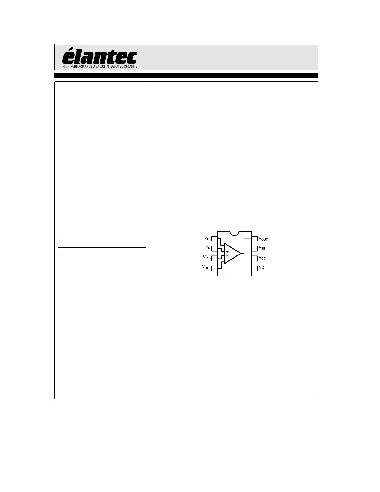
Connection Diagrams
EL2142C SO, P-DIP
Ý
2142-1
Note: All information contained in this data sheet has been carefully checked and is believed to be accurate as of the date of publication; however, this data sheet cannot be a ‘‘controlled document’’. Current revisions, if any, to these
specifications are maintained at the factory and are available upon your request. We recommend checking the revision level before finalization of your design documentation.
©
1996 Elantec, Inc.
Page 2
EL2142C
Differential Line Receiver
Absolute Maximum Ratings
Supply Voltage (V
Maximum Output Current
Storage Temperature Range
Important Note:
All parameters having Min/Max specifications are guaranteed. The Test Level column indicates the specific device testing actually
performed during production and Quality inspection. Elantec performs most electrical tests using modern high-speed automatic test
equipment, specifically the LTX77 Series system. Unless otherwise noted, all tests are pulsed tests, therefore T
Test Level Test Procedure
I 100% production tested and QA sample tested per QA test plan QCX0002.
II 100% production tested at T
III QA sample tested per QA test plan QCX0002.
IV Parameter is guaranteed (but not tested) by Design and Characterization Data.
V Parameter is typical value at T
) 0V to 12.6V
CC–VEE
T
MAX
and T
per QA test plan QCX0002.
MIN
b
A
e
(T
25§C)
A
Operating Junction Temperature
g
60 mA
65§Ctoa150§C
e
25§C and QA sample tested at T
e
25§C for information purposes only.
A
Lead Temperature (
Recommended Operating Temperature
a
k
5 sec)
e
25§C,
A
b
e
T
J
C
150§C
a
300§C
40§Ctoa85§C
e
TA.
DC Electrical Characteristics
ea
(V
CC
5V, V
Parameter Description Min Typ Max
V
supply
I
S
V
OS
I
IN
Z
IN
C
IN
V
DIFF
A
VOL
V
IN
V
OUT
I
(min) Minimum Output Current 50 60 I mA
OUT
V
N
V
REF
PSRR Power Supply Rejection Ratio 60 70 I dB
CMRR2 Input Common Mode Rejection Ratio (V
CMRR1 Input Common Mode Rejection Ratio (full VINrange) 50 60 I dB
eb
EE
5V, T
Supply Operating Range (VCC–VEE)
e
25C, V
A
IN
e
0V, R
e
100, unless otherwise specified)
L
g
3.0
g
5.0
g
Test
Level
Units
6.3 I V
Power Supply Current (no load) 11 14 I mA
Input Referred Offset Voltage
Input Bias Current (VIN,V
INB,VREF
)
b
25 10 40 I mV
b
20 6 20 I m A
Differential Input Resistance 400 V KX
Differential Input Capacitance 1 V pF
Differential Input Range
g
2.0
g
2.3 I V
Open Loop Voltage Gain 75 V dB
Input Common Mode Voltage Range
Output Voltage Swing (50X load to GND)
b
2.6
g
2.9
g
a
4.0 I V
3.1 I V
Input Referred Voltage Noise 36 V nV/SHz
Output Voltage Control Range
b
2.5
e
g
2V) 60 70 I dB
IN
a
3.3 I V
TD is 3.3in
2
Page 3
EL2142C
Differential Line Receiver
AC Electrical Characteristics
ea
(V
5V, V
CC
Parameter Description Min Typ Max
BW(b3dB)
SR Slewrate 400 V V/ms
T
stl
GBWP Gain bandwidth product 200 V MHz
V
BW(b3 dB) V
REF
V
SR V
REF
dG Differential gain at 3.58 MHz. 0.2 V %
di Differential phase at 3.58 MHz. 0.2 V
Pin Description
Pin Number Pin Name Function
1VFBFeedback input
2VINNon-inverting input
3V
4V
5NC
6VCCPositive supply voltage
7VEENegative supply voltage
8V
EE
eb
INB
REF
OUT
e
5V, T
b
Settling time to 1% 15 V ns
REF
REF
25C, V
A
3 dB Bandwidth (Gaine1) 150 V MHz
b
3dB Bandwidth 130 V MHz
Slewrate 100 V V/msec
Inverting input
Sets output voltage level to V
Output voltage
IN
e
0V, R
REF
LOAD
when V
e
100, unless otherwise specified)
e
V
IN
INB
Test
Level
Units
TD is 1.8in
3
Page 4

EL2142C
Differential Line Receiver
Typical Performance Curves
ISvs Supply Voltage
Frequency Response
vs Resistor R1 (Gaine4)
2142– 2
Frequency Response
(Gaine1)
CMRR vs Frequency
2142– 3
V
Frequency Response
REF
2142– 4
2142– 6
Distortion vs Frequency
(GAIN
V
IN
e
e
2V pk/pk
3, R
LOAD
e
100X)
2142– 5
2142– 7
4
Page 5

Applications Information
Gain Equation
V
V
e
((R2aR1)/R1)c(VIN-V
OUT
e
((R2aR1)/R1)c(VIN-V
OUT
a
V
INB
) when R1 tied to V
INB
) when R1 tied to GND
REF
REF
EL2142C
Differential Line Receiver
2142-8
Choice of Feedback Resistor
For a gain of one, V
V
, but 100X –200X improves the bandwidth.
FB
may be shorted back to
OUT
For gains greater than one, there is little to be
gained from choosing resistor R1 value below
200X, for it would only result in increased power
dissipation and potential signal distortion. Above
200X, the bandwidth response will develop some
peaking (for a gain of one), but substantially
higher R1 values may be used for higher voltage
gains, such as up to 1 kX at a gain of four before
peaking will develop.
Capacitance Considerations
As with many high bandwidth amplifiers, the
EL2142C prefers not to drive highly capacitive
loads. It is best if the capacitance on V
OUT
kept below 10 pF if the user does not want gain
peaking to develop. The V
node forms a poten-
FB
tial pole in the feedback loop, so capacitance
should be minimized on this node for maximum
bandwidth.
The amount of capacitance tolerated on any of
these nodes in an actual application will also be
dependent on the gain setting and the resistor
values in the feedback network.
is
5
Page 6

EL2142C
Differential Line Receiver
Typical Applications
Figure 1. Typical Twisted Pair Application
Figure 2. Coaxial Cable Driver
2142-9
2142-10
6
Page 7

EL2142C
Differential Line Receiver
Typical Applications
Ð Contd.
2142-11
Figure 3. Single Supply Receiver
Figure 4. Compensated Line Receiver
7
2142-12
2142-13
Page 8

EL2142C
Differential Line Receiver
EL2142CJanuary 1996 Rev A
Figure 5. Two Channel Multiplexer
General Disclaimer
Specifications contained in this data sheet are in effect as of the publication date shown. Elantec, Inc. reserves the right to make changes
in the circuitry or specifications contained herein at any time without notice. Elantec, Inc. assumes no responsibility for the use of any
circuits described herein and makes no representations that they are free from patent infringement.
WARNING Ð Life Support Policy
Elantec, Inc. products are not authorized for and should not be
used within Life Support Systems without the specific written
consent of Elantec, Inc. Life Support systems are equipment in-
Elantec, Inc.
1996 Tarob Court
Milpitas, CA 95035
Telephone: (408) 945-1323
(800) 333-6314
Fax: (408) 945-9305
European Office: 44-71-482-4596
tended to support or sustain life and whose failure to perform
when properly used in accordance with instructions provided can
be reasonably expected to result in significant personal injury or
death. Users contemplating application of Elantec, Inc. products
in Life Support Systems are requested to contact Elantec, Inc.
factory headquarters to establish suitable terms & conditions for
these applications. Elantec, Inc.’s warranty is limited to replacement of defective components and does not cover injury to persons or property or other consequential damages.
2142-14
Printed in U.S.A.8
 Loading...