

Page 1
EL2099C
Video Distribution Amplifier
EL2099C January 1996 Rev D
Features
# 50 MHzb3 dB bandwidth,
ea
A
2
V
#Differential gain 0.03%
# Differential phase 0.05
§
# Output short circuit current
800 mA
# Can drive six 75 X double
terminated cables
# Slew rate
e
g
11V
1000V/ms
# Wide supply voltage range
g
5V tog15V
Applications
# Video line driver
# ATE pin driver
# High speed data acquisition
Ordering Information
Part No. Temp. Range Pkg. Outline
EL2099CT 0§Ctoa75§C 5-Pin TO-220 MDP0028
General Description
The EL2099C is a high speed, monolithic operational amplifier*
featuring excellent video performance and high output current
capability. Built using Elantec’s Complementary Bipolar process, the EL2099C uses current mode feedback to achieve wide
bandwidth, and is stable in unity gain configuration.
Operation from power supplies ranging from
g
5V tog15V
makes the EL2099C extremely versatile. With supplies at
g
15V, the EL2099C can deliverg11V into 25X at slew rates of
1000V/ms. At
g
5V supplies, output voltage range isg3V into
25X. Its speed and output current capability make this device
ideal for video line driver and automatic test equipment applications.
Differential Gain and Phase of the EL2099C are 0.03% and
0.05
respectively, andb3 dB bandwidth is 50 MHz. These fea-
§
tures make the EL2099C especially well suited for video distribution applications.
Elantec products and facilities comply with MIL-I-45208A, and
other applicable quality specifications. For information on
Ý
Elantec’s processing, see Elantec document, QRA-1: Elantec’s
Processing, Monolithic Integrated Circuits.
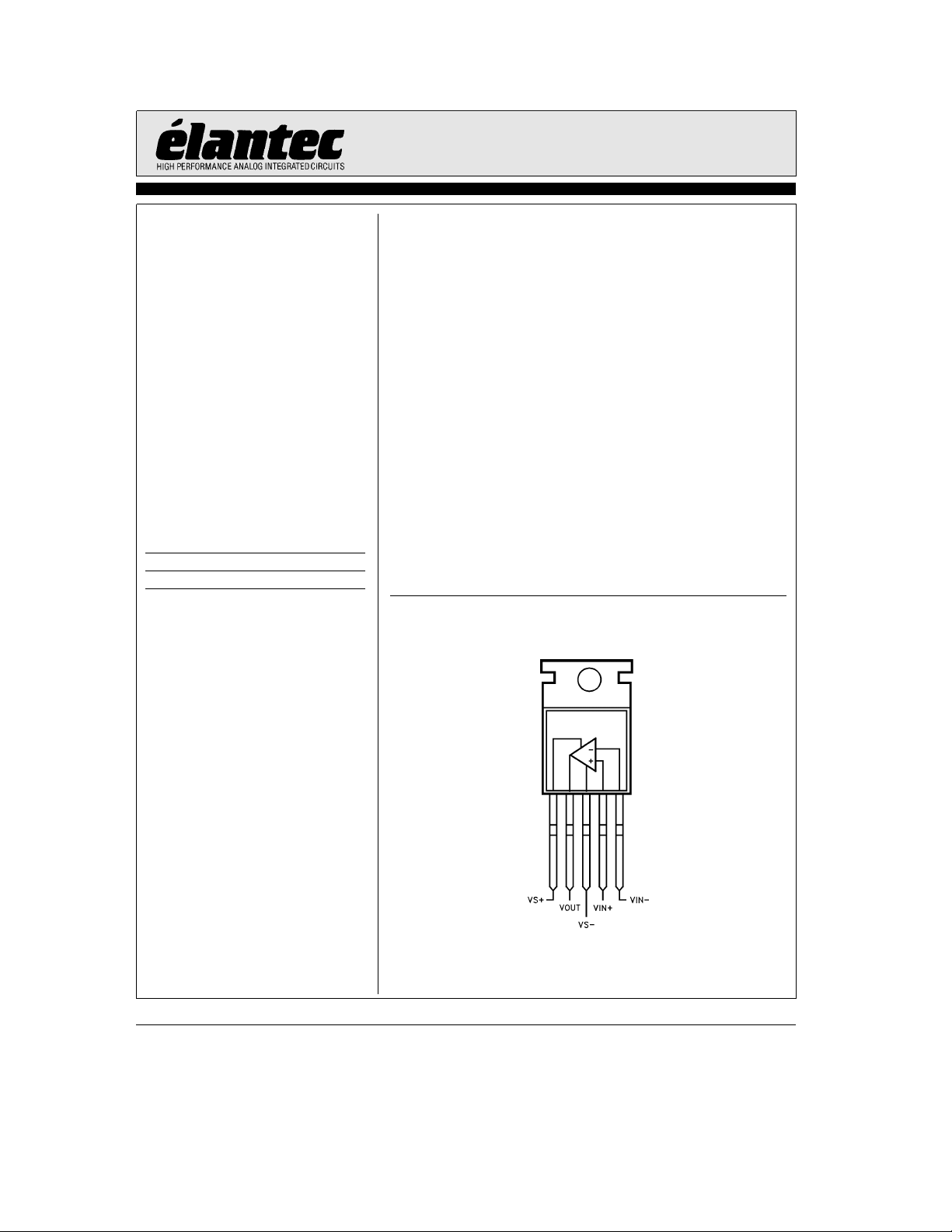
Connection Diagram
5-Pin TO-220
2099– 1
Manufactured under U.S. Patent Nos. 5,179,355, 4,893,091, U.K. Patent No.
2261786.
Note: All information contained in this data sheet has been carefully checked and is believed to be accurate as of the date of publication; however, this data sheet cannot be a ‘‘controlled document’’. Current revisions, if any, to these
specifications are maintained at the factory and are available upon your request. We recommend checking the revision level before finalization of your design documentation.
©
1992 Elantec, Inc.
Page 2
EL2099C
Video Distribution Amplifier
Absolute Maximum Ratings
Voltage between V
Voltage at V
Voltage at V
Voltage between V
Current into V
Important Note:
All parameters having Min/Max specifications are guaranteed. The Test Level column indicates the specific device testing actually
performed during production and Quality inspection. Elantec performs most electrical tests using modern high-speed automatic test
equipment, specifically the LTX77 Series system. Unless otherwise noted, all tests are pulsed tests, therefore T
Test Level Test Procedure
I 100% production tested and QA sample tested per QA test plan QCX0002.
II 100% production tested at T
III QA sample tested per QA test plan QCX0002.
IV Parameter is guaranteed (but not tested) by Design and Characterization Data.
V Parameter is typical value at T
a
S
aa
S
bb
S
IN
or V
a
IN
ba
and V
S
and V
a
T
IN
MAX
b
IN
and T
b
A
per QA test plan QCX0002.
MIN
e
(T
25§C)
A
Internal Power Dissipation See Curves
33V
16.5V
16.5V
g
g
10 mA
e
25§C and QA sample tested at T
e
25§C for information purposes only.
A
Operating Ambient Temperature Range 0
Operating Junction Temperature 150
6V
Storage Temperature Range
Ctoa75§C
§
b
65§Ctoa150§C
e
e
T
TA.
J
C
e
25§C,
A
§
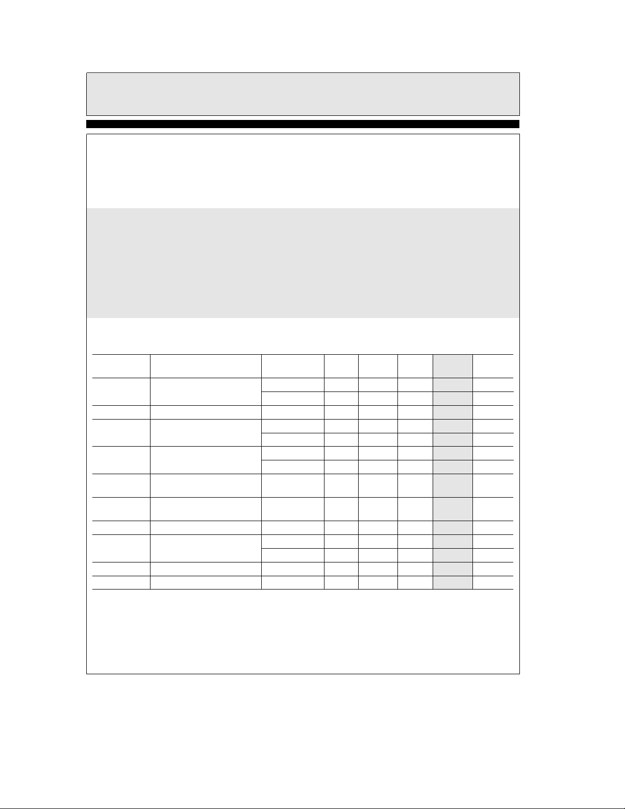
Open Loop DC Electrical Characteristics
e
g
V
S
Parameter Description Temp Min Typ Max
V
OS
TC V
a
I
IN
b
I
IN
CMRR Common Mode Rejection
PSRR Power Supply Rejection
R
OL
a
R
IN
a
C
IN
CMIR Common Mode Input Range 25§C
15V, R
OS
e
L
25X,T
e
25§C unless otherwise specified
A
Test
Level
Units
Input Offset Voltage 25§C 5 20 I mV
T
MIN,TMAX
25 IV mV
Average Offset Voltage Drift Full 20 V mV/§C
a
Input Current 25§C 5 20 I mA
T
MIN,TMAX
b
Input Current 25§C 8 35 I mA
T
MIN,TMAX
25
C5060 IdB
Ratio (Note 1)
Ratio (Note 2)
§
25
C6070 IdB
§
30 IV mA
50 IV mA
Transimpedance 25§C 85 140 I kX
a
Input Resistance 25§C 700 1000 I kX
(Note 3)
a
Input Capacitance 25§C3VpF
T
MIN,TMAX
600 IV kX
g
12.5 V V
C
TDis 3.2in
2
Page 3
EL2099C
Video Distribution Amplifier
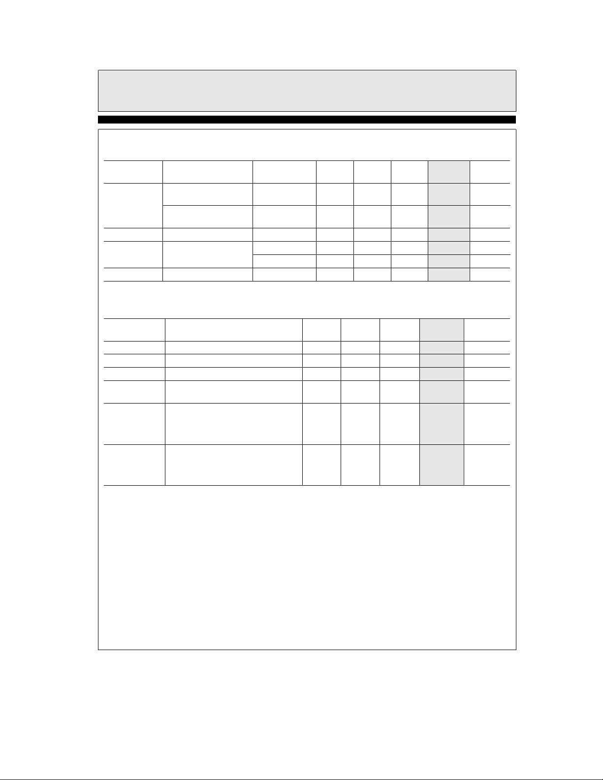
Open Loop DC Electrical Characteristics
e
g
V
S
Parameter Description Temp Min Typ Max
V
O
I
OUT
I
SC
I
S
15V, R
e
L
e
25X,T
25§C unless otherwise specified
A
Output Voltage Swing
e
g
15V
V
S
Output Voltage Swing
e
g
5V
V
S
25
C
§
25
C
§
Output Current 25§C 360 440 I mA
Output Short-Circuit 25§C 600 800 I mA
Current
T
MIN,TMAX
Supply Current 25§C3245ImA
Ð Contd.
g
9
g
2.4
Test
Level
g
11 I V
g
3.0 I V
800 V mA
Closed Loop AC Electrical Characteristics
e
g
V
S
Paremeter Description Min Typ Max
SR Slew Rate (Notes 4, 7) 500 1000 IV V/ms
BW
Peaking (Note 7) 0.3 V dB
tr,t
f
dG Differential Gain; DC Input Offset
dP Differential Phase; DC Input Offset
Note 1: The input is moved fromb10V toa10V.
Note 2: The supplies are moved from
Note 3: V
Note 4: Slew Rate is with V
Note 5: Rise and Fall Times are with V
Note 6: See typical performance curves for other conditions.
Note 7: All AC tests are performed on a ‘‘warmed up’’ part, except for Slew Rate, which is pulse tested.
15V, A
V
ea
e
2, R
510X,R
F
b
3 dB Bandwidth (Note 7) 50 V MHz
e
L
25X,T
e
25§C unless otherwise specified
A
Rise Time, Fall Time
(Notes 5, 7)
from 0V through
Amplitude 286 mV
(Notes 6, 7)
a
0.714V, AC
,fe3.58 MHz
p-p
from 0V througha0.714V, AC
Amplitude 286 mV
(Notes 6, 7)
e
g
5V. See typical performance curve for larger values of VIN.
IN
froma5V tob5V and measured at 20% and 80%.
OUT
,fe3.58 MHz
p-p
g
5V tog15V.
betweenb0.5V anda0.5V and measured at 10% and 90%.
OUT
Test
Level
7Vns
0.03 V %
0.05 V deg. (
Units
Units
TDis 1.7inTDis 2.4in
)
§
3
Page 4
EL2099C
Video Distribution Amplifier
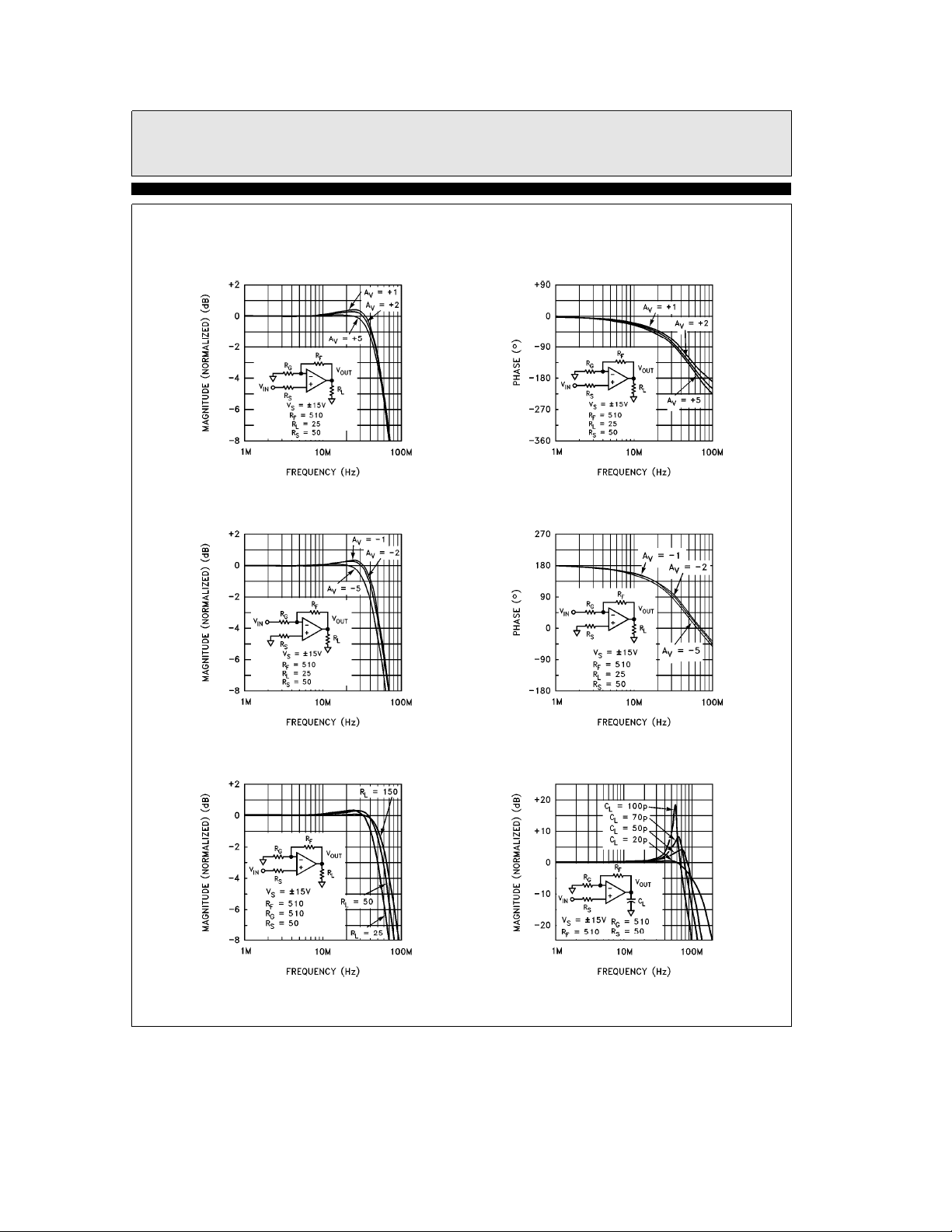
Typical Performance Curves
Non-Inverting
Frequency Response (GAIN)
Inverting Frequency
Response (GAIN)
e
(T
A
25§C, R
L
e
25X,A
V
ea
e
2, R
510 unless otherwise specified)
F
Non-Inverting
Frequency Response (PHASE)
Inverting Frequency
Response (PHASE)
Frequency Response for Various R
L
4
Frequency Response for Various C
L
2099– 2
Page 5
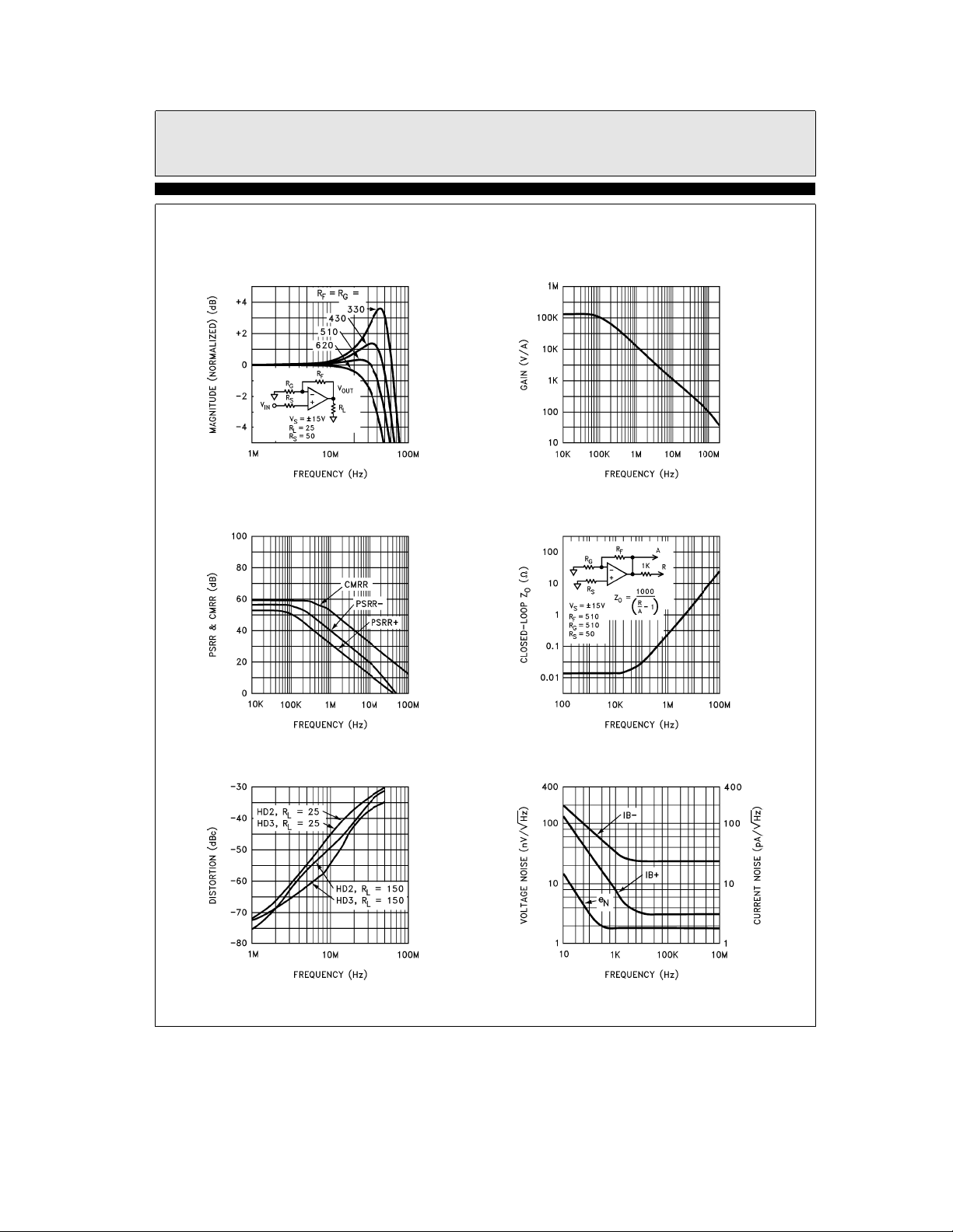
Typical Performance Curves
e
(T
25§C, R
A
e
L
Frequency Response for
Various RF&R
25X,A
V
ea
G
2, R
e
510 unless otherwise specified) Ð Contd.
F
EL2099C
Video Distribution Amplifier
Transimpedance (R
OL
)
PSRR & CMRR vs Frequency Impedance vs Frequency
2nd and 3rd Harmonic
Distortion vs Frequency
Closed-Loop Output
Voltage and Current
Noise vs Frequency
2099– 3
5
Page 6
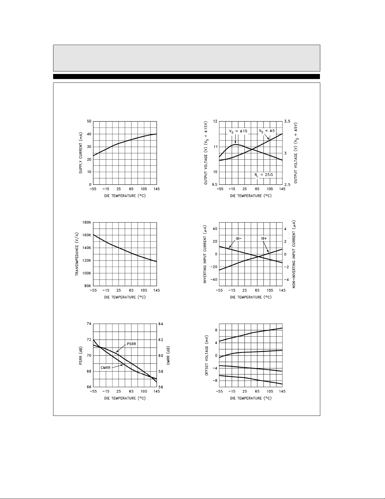
EL2099C
Video Distribution Amplifier
Typical Performance Curves
e
(T
25§C, R
A
L
e
25X,A
V
ea
2, R
e
510 unless otherwise specified) Ð Contd.
F
Supply Current vs
Die Temperature
Transimpedance (R
Die Temperature
OL
)vs
Output Voltage vs
Die Temperature
Input Current vs
Die Temperature
PSRR & CMRR vs
Die Temperature
Offset Voltage vs
Die Temperature
(4 Samples)
2099– 4
6
Page 7
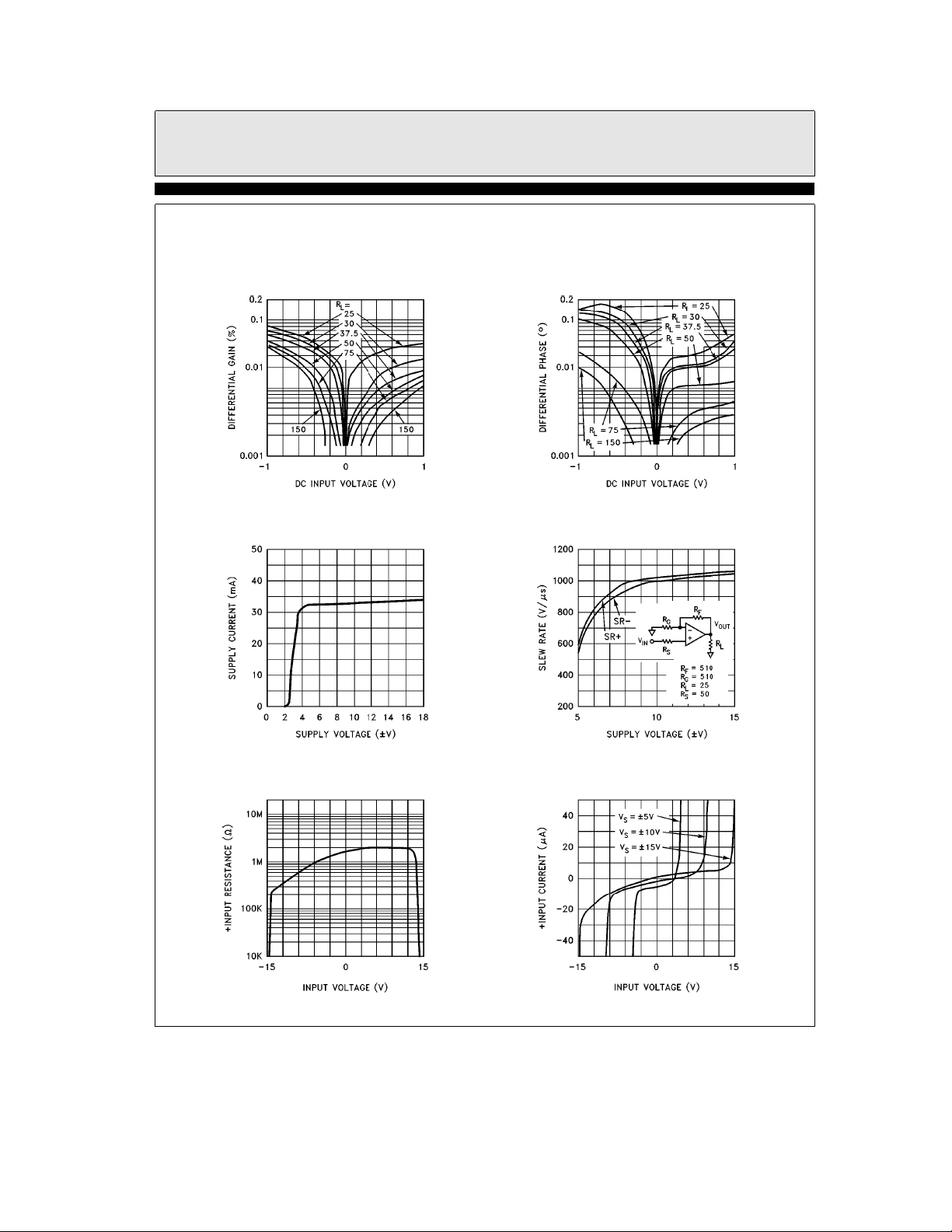
Typical Performance Curves
e
(T
25§C, R
A
e
25X,A
L
Differential Gain vs
DC Input Voltage
for Various RLs
V
ea
2, R
e
510 unless otherwise specified) Ð Contd.
F
EL2099C
Video Distribution Amplifier
Differential Phase vs
DC Input Voltage
for Various R
s
L
Supply Current vs
Supply Voltage
a
Input Resistance
vs Input Voltage
Slew Rate vs
Supply Voltage
a
Input Bias Current
vs Input Voltage
2099– 5
7
Page 8
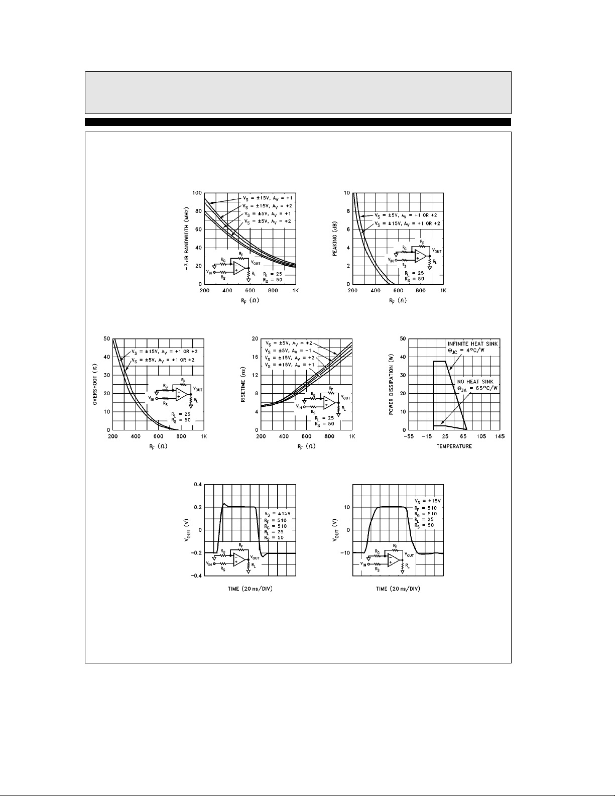
EL2099C
Video Distribution Amplifier
Typical Performance Curves
e
(T
A
25§C, R
Overshoot vs R
L
e
25X,A
F
V
ea
2, R
b
e
510 unless otherwise specified) Ð Contd.
F
3 dB Bandwidth vs R
Rise Time vs R
F
F
Peaking vs R
F
5-Lead TO-220 Maximum
Power Dissipation vs
Ambient Temperature
Small Signal
Pulse Response
Large Signal
Pulse Response
2099– 6
8
Page 9
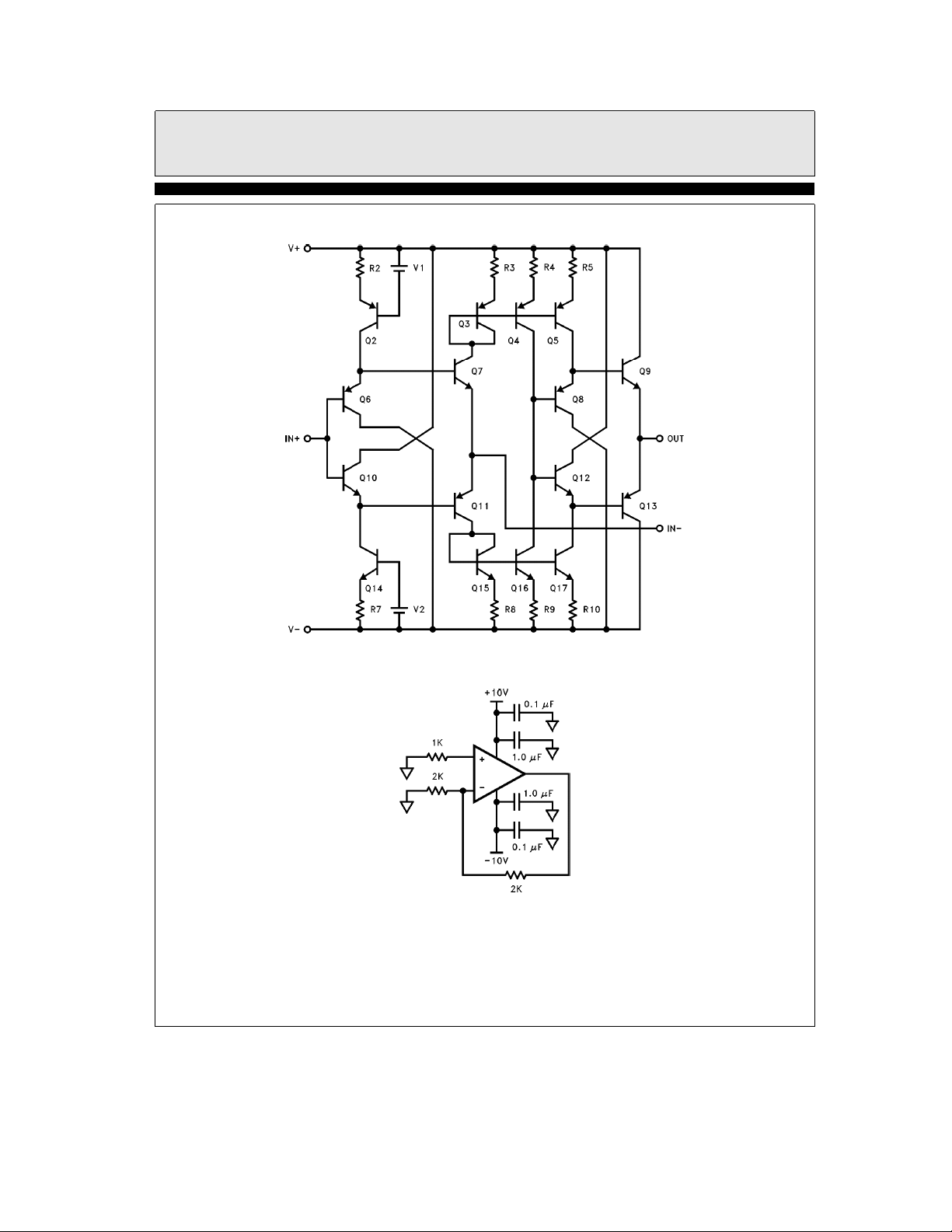
Simplified Schematic
EL2099C
Video Distribution Amplifier
Burn-In Circuit
2099– 7
2099– 8
9
Page 10

EL2099C
Video Distribution Amplifier
Applications Information
Product Description
The EL2099C is a current mode feedback amplifier that has high output current drive capability.
It is built using Elantec’s proprietary dielectric
isolation process that produces NPN and PNP
complimentary transistors. The high output current can be useful to drive many standard video
loads in parallel, as well as digital sync pulses
that are 8V or greater.
a
Input Resistor Value
A small value resistor located in theaInput lead
is necessary to keep the EL2099C from oscillating under certain conditions. A 50X resistor is
recommended for all applications, although
smaller values will work under some circumstances. All tests listed in this datasheet are performed with 50X in the
all typical performance curves. The 50X resistor
along with the
a
additional typical Offset Voltage of only 250 mV
e
at T
25§C, and a maximum of 1.25 mV over
temperature variations.
Feedback Resistor Values
The EL2099C has been designed and specified
with R
e
F
510X and A
feedback resistor yields extremely flat frequency
response with little to no peaking. However, 3 dB
bandwidth is reduced somewhat because of this.
Wider bandwidth, at the expense of slight peaking, can be accomplished by reducing the value of
the feedback resistor. For example, at a gain of
a
2, reducing the feedback resistor to 330X in-
creases the
b
3 dB bandwidth to 70 MHz with
3 dB of peaking. Inversely, larger values of feedback resistor will cause roll off to occur at a lower
frequency. There is essentially no peaking with
l
R
510X.
F
Power Supplies
The EL2099C may be operated with single or
split supplies as low as
high as
g
18V (36V total). Bandwidth and slew
rate are almost constant from V
a
Input lead, as well as
Input bias current creates an
ea
V
2. This value of
g
5V (10V total) to as
e
g
S
10V to
g
18V, and decrease slightly as supplies are re-
duced to
g
5V, as shown in the characteristic
curves. It is not necessary to use equal value split
supplies. For example,
b
5V andb12V would be
fine for 0V to 1V video signals.
Good power supply bypassing should be used to
reduce the risk of oscillation. A 1 mFto10mF
tantalum capacitor in parallel with a 0.1 mF ceramic capacitor is recommended for bypassing
each supply pin. They should be kept as close as
possible to the device pins.
Due to the internal construction of the TO-220
package, the tab of the EL2099C is connected to
the V
pin. Therefore, care must be taken to
b
S
avoid connecting the tab to the ground plane of
the system.
Printed Circuit Board Layout
As with any high frequency device, good printed
circuit board layout is necessary for optimum
performance. Ground plane construction is highly recommended. Lead lengths should be as short
as possible. For good AC performance, parasitic
capacitances should be kept to a minimum, especially at the inverting input, which is sensitive to
stray capacitance. This implies keeping the
ground plane away from this pin. Metal film and
carbon resistors are both acceptable, while use of
wire-wound resistors is not recommended because of their parasitic inductance. Similarly, capacitors should be low inductance for best performance.
Driving Cables and Capacitive Loads
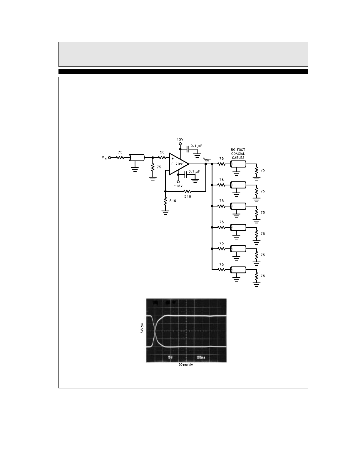
The EL2099C was designed with driving multiple coaxial cables in mind. With 440 mA of output drive and low output impedance, driving six
75X double terminated coaxial cables to
g
11V
with one EL2099C is practical.
When used as a cable driver, double termination
is always recommended for reflection-free performance. For those applications, the back termination series resistor will decouple the EL2099C
from the capacitive cable and allow extensive capacitive drive. For a discussion on some of the
other ways to drive cables, see the application
section on driving cables in the EL2003 data
sheet.
10
Page 11
EL2099C
Video Distribution Amplifier
Applications Information
Other applications may have high capacitive
loads without termination resistors. In these applications, an additional small value (5X –50X)
resistor in series with the output will eliminate
most peaking.
Ð Contd.
The schematic below shows the EL2099C driving
6 double terminated cables, each of average
length of 50 feet.
This represents driving an effective load of 25X
to over
shown in the scope photo. Notice that double termination results in reflection free performance.
g
10V. The resulting performance is
2099– 10
2099– 11
11
Page 12

EL2099C
Video Distribution Amplifier
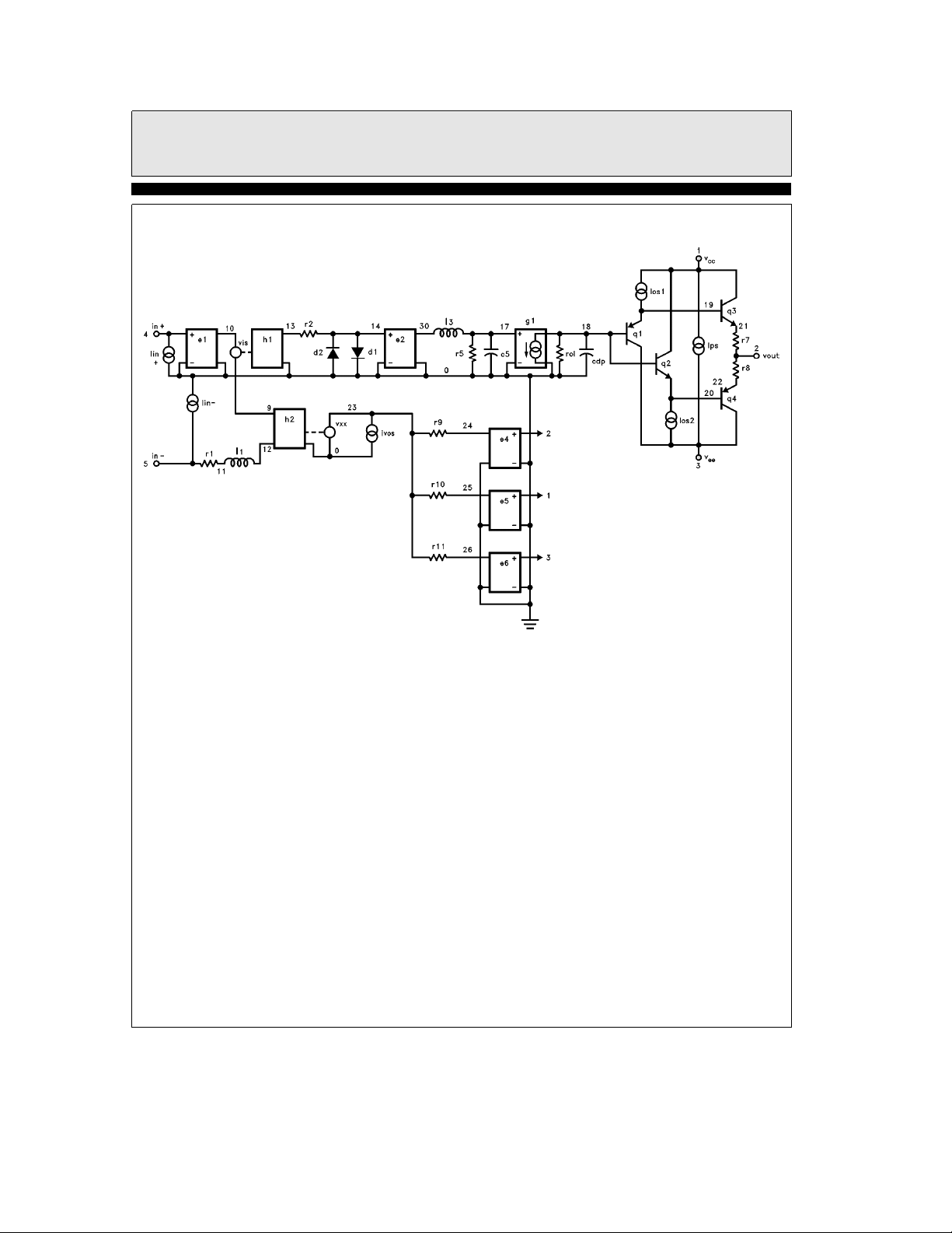
EL2099 Macromodel
* Connections:
*
*
*
*
*
.subckt M2099 4 5132
*
*Input Stage
*
e1100401.0
vis 10 9 0V
h2 9 12 vxx 1.0
r151150
l1 11 12 48nH
iinp405mA
b
iinm 5 0
*
* Slew Rate Limiting
*
h1 13 0 vis 600
r2 13 14 1K
d1 14 0 dclamp
d2 0 14 dclamp
*
* High Frequency Pole
*
*e2 30 0 14 0 0.001667
13 30 17 1.5mH
c5 17 0 1pF
r5 17 0 500
*
* Transimpedance Stage
*
g10181701.0
ro1 18 0 150K
cdp 18 0 8pF
*
* Output Stage
*
q131819qp
q211820qn
q311921qn
q432022qp
r7 21 2 1
r8 22 2 1
a
input
b
input
l
ll
lll
llll
a
Vsupply
b
Vsupply
output
lllll
8mA
TABWIDE
TDis 6.1in
12
Page 13

EL2099C
Video Distribution Amplifier
EL2099 Macromodel
ios1 1 19 5mA
ios2 20 3 5mA
*
* Supply Current
*
ips 1 3 19mA
*
* Error Terms
*
ivos 0 23 5mA
vxx 23 0 0V
e4240201.0
e5250101.0
e6260301.0
r9 24 23 3K
r10 25 23 1K
r11 26 23 1K
* Models
*
.model qn npn (is
.model qp pnp (is
.model dclamp d (is
.ends
e5eb
15 bfe200 tfe0.1nS)
e5eb
15 bfe200 tfe0.1nS)
e1eb
30 ibve0.266 bve5ne4)
Ð Contd.
TDis 3.1in
13
Page 14
EL2099C
Video Distribution Amplifier
EL2099 Macromodel
Ð Contd.
2099– 9
14
Page 15

BLANK
15
Page 16
EL2099C
Video Distribution Amplifier
EL2099CJanuary 1996 Rev D
General Disclaimer
Specifications contained in this data sheet are in effect as of the publication date shown. Elantec, Inc. reserves the right to make changes
in the circuitry or specifications contained herein at any time without notice. Elantec, Inc. assumes no responsibility for the use of any
circuits described herein and makes no representations that they are free from patent infringement.
WARNING Ð Life Support Policy
Elantec, Inc. products are not authorized for and should not be
used within Life Support Systems without the specific written
consent of Elantec, Inc. Life Support systems are equipment in-
Elantec, Inc.
1996 Tarob Court
Milpitas, CA 95035
Telephone: (408) 945-1323
(800) 333-6314
Fax: (408) 945-9305
European Office: 44-71-482-4596
tended to support or sustain life and whose failure to perform
when properly used in accordance with instructions provided can
be reasonably expected to result in significant personal injury or
death. Users contemplating application of Elantec, Inc. products
in Life Support Systems are requested to contact Elantec, Inc.
factory headquarters to establish suitable terms & conditions for
these applications. Elantec, Inc.’s warranty is limited to replacement of defective components and does not cover injury to persons or property or other consequential damages.
Printed in U.S.A.16
 Loading...