

Page 1
EL2070C
200MHz Current Feedback Amplifier
EL2070C
Features
• 200MHz -3dB bandwidth, AV=2
• Disable/enable
• 12ns settling to 0.05%
• VS = ±5V @ 15mA
• Low distortion: HD2, HD3 @ -----
-60dBc at 20MHz
• Differential gain 0.02% at NTSC,
PAL
• Differential phase 0.01° at NTSC,
PAL
• Overload/short-circuit protected
• ±1 to ±8 closed-loop gain range
• Low cost
Applications
• Video gain block
• Video distribution
• HDTV amplifier
• Analog multiplexing (using
disable)
• Power-down mode (using disable)
• High-speed A/D conversion
• D/A I-V conversion
• Photodiode, CCD preamps
• IF processors
• High-speed communications
General Description
The EL2070C is a wide bandwidth, fast settling monolithic amplifier
incorporating a disable/enable feature. Built using an advanced complementary bipolar process, this amplifier uses current-mode feedback
to achieve more bandwidth at a given gain than conventional operational amplifiers. Designed for closed-loop gains of ±1 to ±8, the
EL2070C has a 200MHz -3dB bandwidth (AV = +2), and 12ns settling
to 0.05% while consuming only 15mA of supply current. Furthermore,
the fast disable/enable times of 200ns/100ns allow rapid analog
multiplexing.
The EL2070C is an obvious high-performance solution for video distribution and line-driving applications, especially when its disable
feature can be used for fast analog multiplexing. Furthermore, the low
15mA supply current, and the very low 5mA of supply current when
disabled suggest use in systems where power is critical. With differential gain/phase of 0.02%/0.01°, guaranteed video specifications, and a
minimum 50mA output drive, performance in these areas is assured.
The EL2070C's settling to 0.05% in 12ns, low distortion, and ability to
drive capacitive loads make it an ideal flash A/D driver. The wide
200MHz bandwidth and extremely linear phase allow unmatched signal fidelity. D/A systems can also benefit from the EL2070C,
especially if linearity and drive levels are important.
Ordering Information
Part No. Temp. Range Package Outline #
EL2070CN -40°C to +85°C 8-Pin P-DIP MDP0031
EL2070CS -40°C to +85°C 8-Lead SO MDP0027
Note: All information contained in this data sheet has been carefully checked and is believed to be accurate as of the date of publication; however, this data sheet cannot be a “controlled document”. Current revisions, if any, to these
specifications are maintained at the factory and are available upon your request. We recommend checking the revision level before finalization of your design documentation.
© 2001 Elantec Semiconductor, Inc.
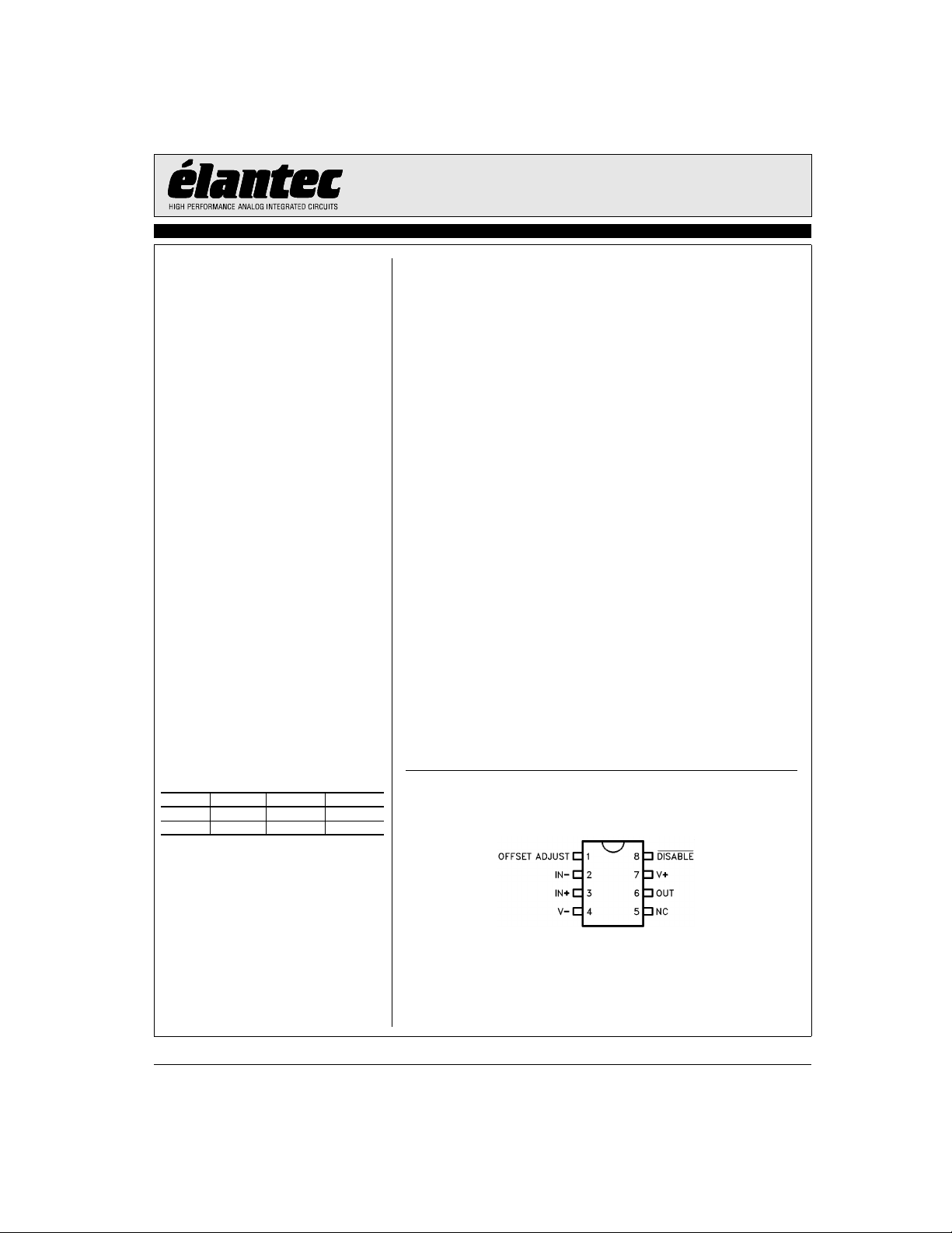
Connection Diagrams
DIP and SO Package - Top VIew
Manufactured under U.S. Patent No. 4,893,091
September 26, 2001
Page 2
EL2070C
200MHz Current Feedback Amplifier
EL2070C
Absolute Maximum Ratings (T
Supply Voltage (VS) ±7V
Output Current 70mA
(Output is short-circuit protected to ground, however,
maximum reliability is obtained if I
Common-Mode Input Voltage ±V
Differential Input Voltage 5V
Disable Input Voltage +VS, -1V
Thermal Resistance θ
does not exceed 70mA)
OUT
= 25°C)
A
= 95°C/W P-DIP
JA
θ
JA
Applied Output Voltage (Disabled) ±V
Power Dissipation See Curves
Operating Temperature
S
EL2070C -40C to +85C
Lead Temperature (Soldering, 5 Seconds) 300°C
Junction Temperature 175°C
Storage Temperature-60°C to +150°C
= 175°C/W SO-8
Important Note:
All parameters having Min/Max specifications are guaranteed. Typ values are for information purposes only. Unless otherwise noted, all tests are at the
specified temperature and are pulsed tests, therefore: TJ = TC = TA.
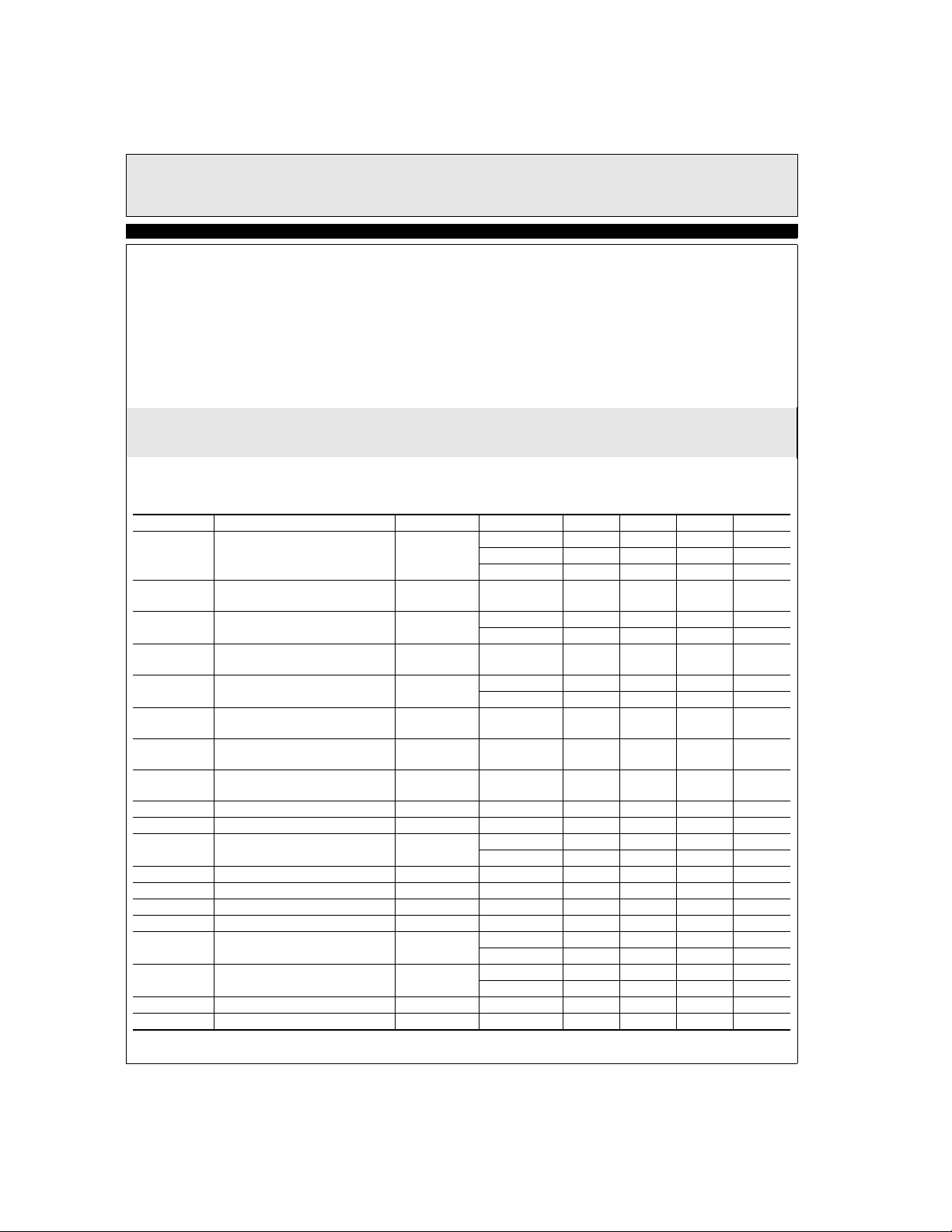
Open Loop DC Electrical Characteristics
VS = ±5V, R
V
d(VOS)/dT Average Offset
+I
d(+IIN)/dT Average +Input
-I
d(-IIN)/dT Average -Input
PSRR Power Supply
CMRR Common-Mode
I
S
IS
+R
C
R
R
C
CMIR Common-Mode
I
OUT
V
V
= 100Ω unless otherwise specified
L
Parameter Description Test Conditions Temp Min Typ Max Unit
OS
Input Offset Voltage 25°C 2 5.5 mV
T
MIN
T
[1]
MAX
All 10.0 40.0 µV/°C
8.2 mV
9.0 mV
Voltage Drift
IN
+Input Current 25°C, T
[1]
T
All 50.0 200.0 nA/°C
MAX
MIN
10 25.0 µA
36.0 µA
Current Drift
IN
-Input Current 25.0°C 10 30 µA
T
, T
MIN
[1]
MAX
All 50.0 200.0 nA/°C
46 µA
Current Drift
All 45.0 50.0 dB
Rejection Ratio
All 40.0 50.0 dB
Rejection Ratio
Supply Current—Quiescent No Load All 16.0 20.0 mA
OFF
IN
IN
OUT
D Output Resistance (DC) Disabled All 100.0 200.0 kΩ
OUT
D Output Capacitance (DC) Disabled All 0.5 2.0 pF
OUT
Supply Current—Disabled
+Input Resistance 25°C, T
Input Capacitance All 0.5 2.0 pF
Output Impedance (DC) All 0.1 0.2 Ω
Input Range
Output Current 25°C, T
OUT
L Output Voltage Swing 100Ω 25°C 3.0 3.4 V
OUT
Output Voltage Swing No Load All 3.3 3.5 V
[2]
[3]
All 4.0 7.0 mA
100.0 200.0 kΩ
50.0 kΩ
2.0 2.1 V
1.2 V
50.0 70.0 mA
35.0 mA
T
25°C, T
T
T
MAX
MIN
MAX
MIN
MAX
MIN
S
2
Page 3
EL2070C
200MHz Current Feedback Amplifier
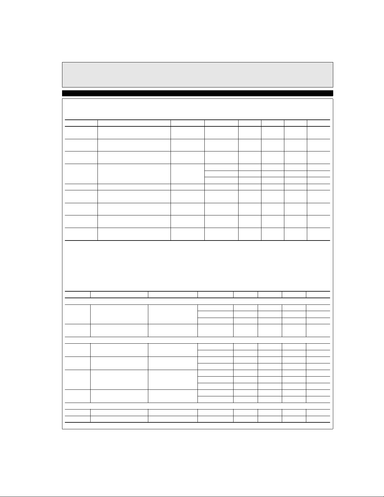
Open Loop DC Electrical Characteristics (Continued)
VS = ±5V, R
-ICMR Input Current Common
+IPSR +Input Current Power
-IPSR -Input Current Power
R
OL
I
LOGIC
V
V
I
DIS
I
EN
1. Measured from T
2. Supply current when disabled is measured at the negative supply.
3. Common-mode input range for rated performance.
= 100Ω unless otherwise specified
L
Parameter Description Test Conditions Temp Min Typ Max Unit
25°C 8.0 33.0 µA/V
Mode Rejection
25°C 1.0 3.6 µA/V
Supply Rejection
25°C 20 24 µA/V
Supply Rejection
Transimpedance 25°C 30.0 125.0 V/mA
T
T
MIN
MAX
80.0 V/mA
140.0 V/mA
Pin 8 Current @ 0V All 0.8 1.2 mA
DIS
Maximum Pin 8
All 0.5 V
V to Disable
EN
Minimum Pin 8
All 3.5 V
V to Enable
Minimum Pin 8
All 350.0 µA
I to Disable
Maximum Pin 8
All 60.0 µA
I to Enable
to T
MAX
.
MIN
EL2070C
Closed-Loop AC Electrical Characteristics
VS = ±5V, R
Parameter Description Test Conditions Temp Min Typ Max Unit
FREQUENCY RESPONSE
SSBW -3dB Bandwidth
LSBW -3dB Bandwidth
GAIN FLATNESS
GFPL Peaking
GFPH Peaking
GFR Rolloff
LPD Linear Phase Deviation
TIME-DOMAIN RESPONSE
tr1, t
tr2, t
= 250Ω, A
F
= +2, R
= 100Ω unless otherwise specified
V
L
25°C 150.0 200.0 MHz
(V
< 0.5VPP)
OUT
T
T
MIN
MAX
150.0 MHz
120.0 MHz
AV = +5 All 35.0 50.0 MHz
(V
< 5.0VPP)
OUT
<40MHz 25°C 0.0 0.3 dB
V
< 0.5V
OUT
PP
T
, T
MIN
MAX
>40MHz 25°C 0.0 0.5 dB
V
< 0.5V
OUT
PP
T
, T
MIN
MAX
<75MHz 25°C 0.6 1.0 dB
V
< 0.5V
OUT
V
OUT
Rise Time, Fall Time 0.5V Step All 1.6 2.4 ns
f1
Rise Time, Fall Time 5.0V Step All 6.5 10.0 ns
f2
< 0.5V
PP
<75MHz 25°C, T
PP
T
T
T
MIN
MAX
MAX
MIN
0.2 1.0 °
3
0.4 dB
0.7 dB
1.0 dB
1.3 dB
1.2 °
Page 4
EL2070C
200MHz Current Feedback Amplifier
EL2070C
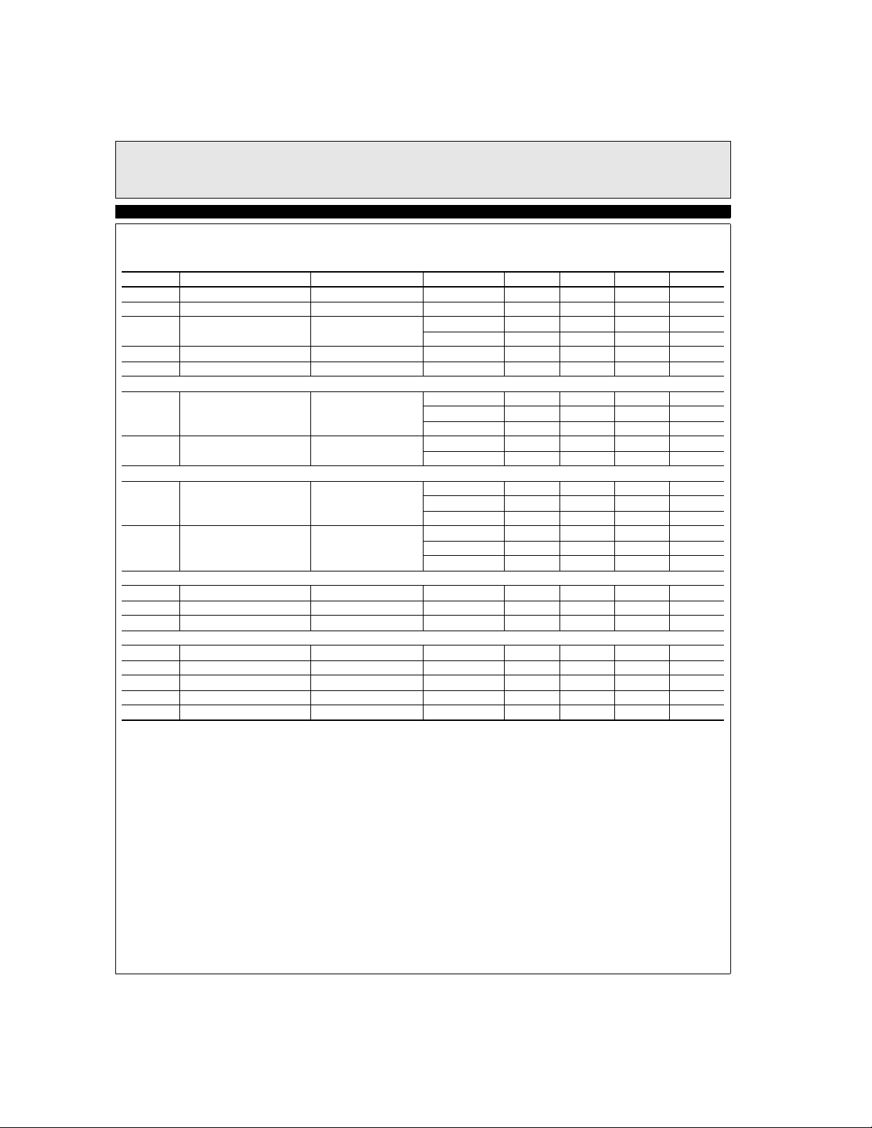
Closed-Loop AC Electrical Characteristics
VS = ±5V, R
Parameter Description Test Conditions Temp Min Typ Max Unit
t
s1
t
s2
OS Overshoot 0.5V Step 25°C, T
SR Slew Rate AV = +2 All 430.0 700.0 V/µs
DISTORTION
HD2 2nd Harmonic Distortion
HD3 3rd Harmonic Distortion
EQUIVALENT INPUT NOISE
NF Noise Floor
INV Integrated Noise
DISABLE/ENABLE PERFORMANCE
T
T
OFFIso Off Isolation 10MHz All 55.0 59.0 dB
VIDEO PERFORMANCE
d
G
d
P
d
G
d
P
VBW -0.1dB Bandwidth
= 250Ω, A
F
= +2, R
= 100Ω unless otherwise specified
V
L
Settling Time to 0.1% 2.0V Step All 10.0 13.0 ns
Settling Time to 0.05% 2.0V Step All 12.0 15.0 ns
AV = - 2 All 1600.0 V/µs
2V
PP
at 20MHz
2V
PP
at 20MHz
[1]
>100kHz
[1]
100kHz to 200MHz
OFF
ON
Disable Time to >50dB 10MHz All 1000.0 IV ns
Enable Time All 200.0 ns
Differential Gain
Differential Phase
Differential Gain
Differential Phase
[2]
[2]
[2]
[2]
[2]
NTSC/PAL 25°C 0.02 0.08 % pp
NTSC/PAL 25°C 0.01 0.08 ° pp
30MHz 25°C 0.05 0.18 % pp
30MHz 25°C 0.05 0.18 ° pp
1. Noise Tests are performed from 5MHz to 200MHz.
2. Differential gain/phase tests are with R
= 100Ω. For other values of R
L
, see curves.
L
MAX
T
MIN
0.0 10.0 %
15.0 %
25°C -60.0 -45.0 dBc
T
T
MIN
MAX
-40.0 dBc
-45.0 dBc
25°C -60.0 -50.0 dBc
T
MIN
, T
MAX
-50.0 dBc
25°C -157.0 -154.0 dBm (1Hz)
T
T
MIN
MAX
-154.0 dBm (1Hz)
-153.0IV dBm (1Hz)
25°C 40.0 57.0 µV
T
T
MIN
MAX
57.0 µV
63.0 µV
25°C 30.0 60.0 MHz
4
Page 5
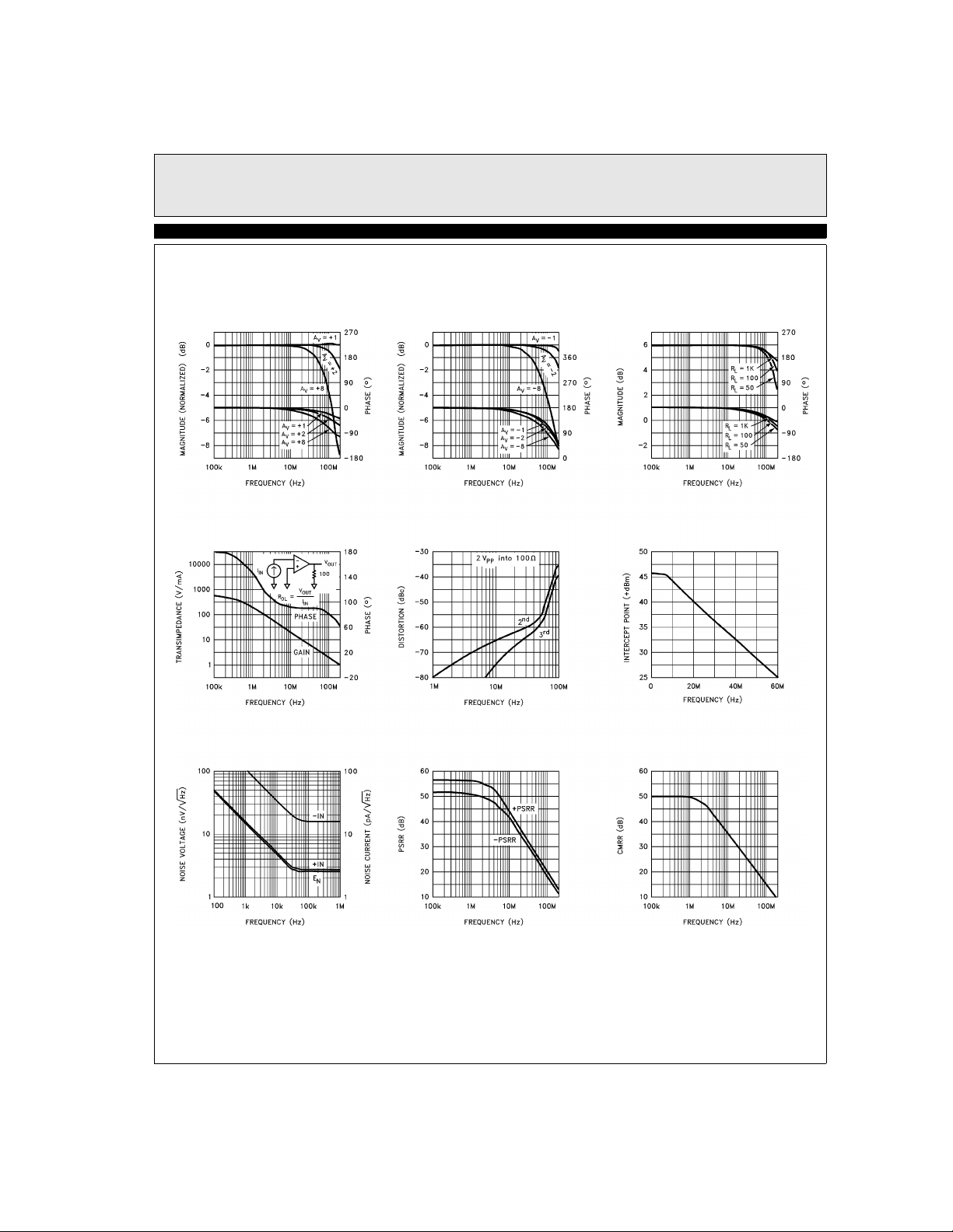
Typical Performance Curves
EL2070C
EL2070C
200MHz Current Feedback Amplifier
Non-Inverting
Frequency Response
Open-Loop Transimpedance
Gain and Phase
Equivalent Input Noise Power-Supply
Inverting
Frequency Response
2nd and 3rd
Harmonic Distortion
Rejection Ratio
Frequency Response for
Various RLs
2-Tone 3rd Order
Intermodulation Intercept
Common-Mode
Rejection Ratio
5
Page 6
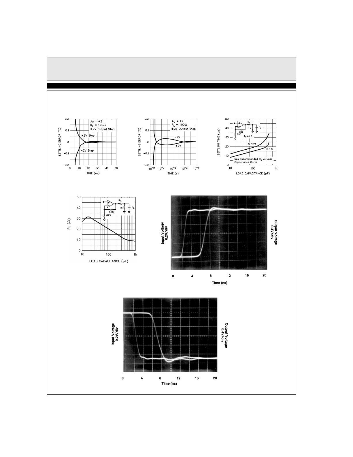
EL2070C
200MHz Current Feedback Amplifier
EL2070C
Settling Time Long-Term Settling Time Settling Time vs
Recommended RS vs
Load Capacitance
Pulse Response AV = +2
Load Capacitance
Pulse Response AV = +2
6
Page 7
EL2070C
200MHz Current Feedback Amplifier
EL2070C
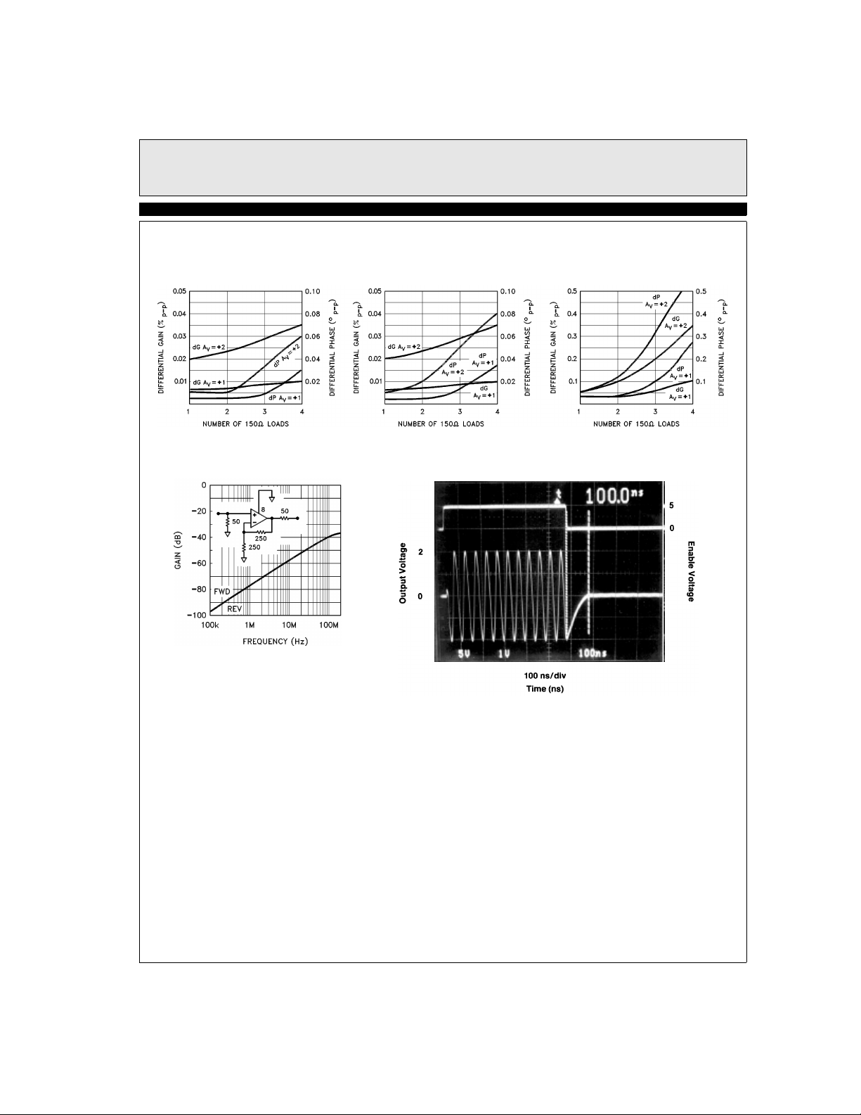
Differential Gain and
Phase (3.58MHz)
Forward and Reverse Gain
during Disable
Differential Gain and
Phase (4.43MHz)
Enable/Disable Response
Differential Gain and
Phase (30MHz)
7
Page 8
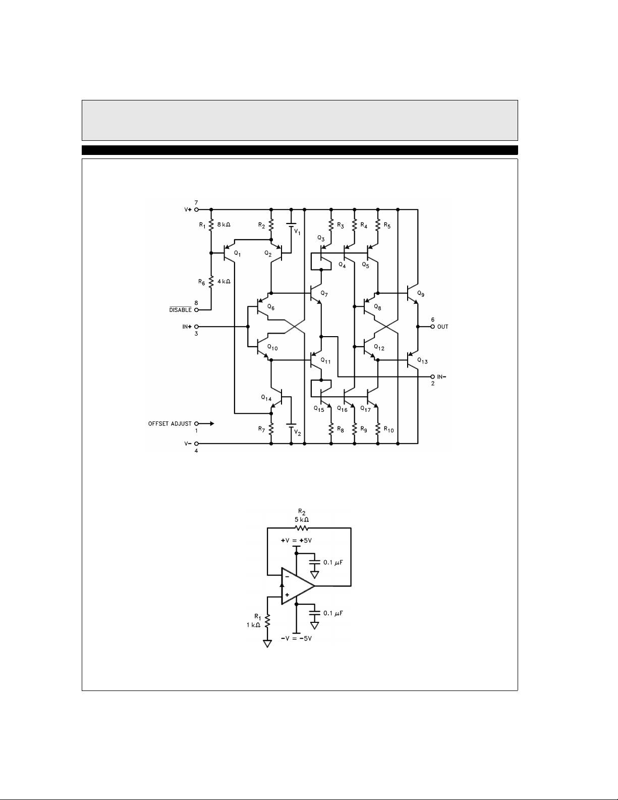
EL2070C
200MHz Current Feedback Amplifier
EL2070C
Equivalent Circuit
Burn-In Circuit
ALL PACKAGES USE THE SAME SCHEMATIC.
8
Page 9

Applications Information
EL2070C
EL2070C
200MHz Current Feedback Amplifier
Theory of Operation
The EL2070C has a unity gain buffer from the noninverting input to the inverting input. The error signal of
the EL2070C is a current flowing into (or out of) the
inverting input. A very small change in current flowing
through the inverting input will cause a large change in
the output voltage. This current amplification is called
the transimpedance (ROL) of the EL2070C
[V
=(ROL) * (-IIN)]. Since ROL is very large, the cur-
OUT
rent flowing into the inverting input in the steady-state
(non-slewing) condition is very small.
Therefore we can still use op-amp assumptions as a firstorder approximation for circuit analysis, namely that:
1.The voltage across the inputs is approximately 0V.
2.The current into the inputs is approximately 0mA.
Resistor Value Selection and Optimization
The value of the feedback resistor (and an internal
capacitor) sets the AC dynamics of the EL2070C. The
nominal value for the feedback resistor is 250Ω, which
is the value used for production testing. This value guarantees stability. For a given closed-loop gain the
bandwidth may be increased by decreasing the feedback
resistor and, conversely, the bandwidth may be
decreased by increasing the feedback resistor.
Reducing the feedback resistor too much will result in
overshoot and ringing and eventually oscillations.
Increasing the feedback resistor results in a lower -3dB
frequency. Attenuation at high frequency is limited by a
zero in the closed-loop transfer function which results
from stray capacitance between the inverting input and
ground. Consequently, it is very important to keep stray
capacitance to a minimum at the inverting input.
Differential Gain/Phase
An industry-standard method of measuring the distortion of a video component is to measure the amount of
differential gain and phase error it introduces. To measure these, a 40 IREPP reference signal is applied to the
device with 0V DC offset (0 IRE) at 3.58MHz for
NTSC, 4.43MHz for PAL, and 30MHz for HDTV. A
second measurement is then made with a 0.714V DC
offset (100 IRE). Differential Gain is a measure of the
change in amplitude of the sine wave, and is measured in
percent. Differential Phase is a measure of the change in
phase, and is measured in degrees. Typically, the maximum positive and negative deviations are summed to
give peak values.
In general, a back terminated cable (75Ω in series at the
drive end and 75Ω to ground at the receiving end) is pre-
ferred since the impedance match at both ends will
absorb any reflections. However, when double-termination is used, the received signal is reduced by half;
therefore a gain of 2 configuration is typically used to
compensate for the attenuation. In a gain of 2 configuration, with output swing of 2VPP, with each back-
terminated load at 150Ω. The EL2070C is capable of
driving up to 4 back-terminated loads with excellent
video performance. Please refer to the typical curves for
more information on video performance with respect to
frequency, gain, and loading.
Capacitive Feedback
The EL2070C relies on its feedback resistor for proper
compensation. A reduction of the impedance of the feedback element results in less stability, eventually
resulting in oscillation. Therefore, circuit implementations which have capacitive feedback should not be used
because of the capacitor's impedance reduction with frequency. Similarly, oscillations can occur when using the
technique of placing a capacitor in parallel with the feedback resistor to compensate for shunt capacitances from
the inverting input to ground.
Offset Adjustment Pin
Output offset voltage of the EL2070C can be nulled by
tying a 10k potentiometer between +VS and -VS with the
slider attached to pin 1. A full-range variation of the
voltage at pin 1 to ±5V results in an offset voltage
adjustment of at least ±10mV. For best settling performance pin 1 should be bypassed to ground with a
ceramic capacitor located near to the package, even if
the offset voltage adjustment feature is not being used.
9
Page 10

EL2070C
200MHz Current Feedback Amplifier
EL2070C
Printed Circuit Layout
As with any high frequency device, good PCB layout is
necessary for optimum performance. Ground plane construction is a requirement, as is good power-supply and
Offset Adjust bypassing close to the package. The
inverting input is sensitive to stray capacitance, therefore connections at the inverting input should be
minimal, close to the package, and constructed with as
little coupling to the ground plane as possible.
Capacitance at the output node will reduce stability,
eventually resulting in peaking, and finally oscillation if
the capacitance is large enough. The design of the
EL2070C allows a larger capacitive load than comparable products, yet there are occasions when a series
resistor before the capacitance may be needed. Please
refer to the graphs to determine the proper resistor value
needed.
Disable/Enable Operation
The EL2070C has a disable/enable control input at pin 8.
The device is enabled and operates normally when pin 8
is left open or tied to pin 7. When more than 350µA is
pulled from pin 8, the EL2070C is disabled. The output
becomes a high impedance, the inverting input is no
longer driven to the positive input voltage, and the supply current is reduced by 2/3. To make it easy to use this
feature, there is an internal resistor to limit the current to
a safe level (0.8mA) if pin 8 is grounded.
To draw current out of pin 8 an open-collector TTL output, a 5V CMOS output, or an NPN transistor can be
used.
10
Page 11

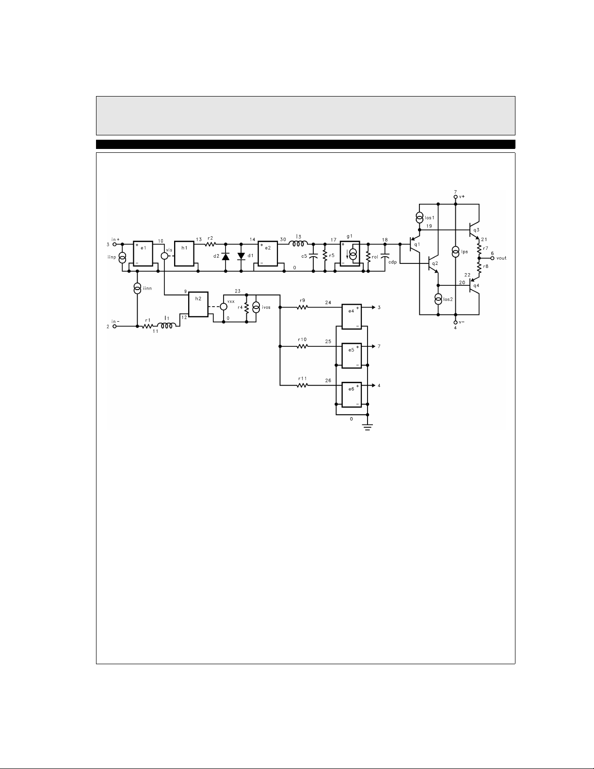
EL2070C Macromodel
* Revision A. March 1992
* Enhancements include PSRR, CMRR, and Slew Rate Limiting
* Connections: +input
* | -input
* | | +Vsupply
* | | | -Vsupply
* | | | | output
* | | | | |
.subckt M2070C 3 2 7 4 6
*
* Input Stage
*
e1 10 0 3 0 1.0
vis 10 9 0V
h2 9 12 vxx 1.0
r1 2 11 50
l1 11 12 48nH
iinp 3 0 8µA
iinm 2 0 8µA
*
* Slew Rate Limiting
*
h1 13 0 vis 600
r2 13 14 1K
d1 14 0 dclamp
d2 0 14 dclamp
*
* High Frequency Pole
*
e2 30 0 14 0 0.00166666666
l3 30 17 0.1µH
c5 17 0 0.1pF
r5 17 0 500
*
* Transimpedance Stage
*
g1 0 18 17 0 1.0
rol 18 0 150K
cdp 18 0 2.8pF
*
* Output Stage
*
q1 4 18 19 qp
q2 7 18 20 qn
q3 7 19 21 qn
q4 4 20 22 qp
r7 21 6 2
r8 22 6 2
ios1 7 19 2.5mA
ios2 20 4 2.5mA
*
* Supply Current
*
ips 7 4 9mA
*
* Error Terms
*
ivos 0 23 5mA
vxx 23 0 0V
e4 24 0 3 0 1.0
e5 25 0 7 0 1.0
EL2070C
EL2070C
200MHz Current Feedback Amplifier
11
Page 12

EL2070C
200MHz Current Feedback Amplifier
EL2070C
e6 26 0 4 0 1.0
r9 24 23 3K
r10 25 23 1K
r11 26 23 1K
*
* Models
*
.model qn npn (is=5e-15 bf=200 tf=0.05nS)
.model qp pnp (is=5e-15 bf=200 tf=0.05nS)
.model dclamp d(is=1e-30 ibv=0.266 bv=1.3 n=4)
.ends
12
Page 13
EL2070C Macromodel
EL2070C
EL2070C
200MHz Current Feedback Amplifier
13
Page 14
EL2070C
200MHz Current Feedback Amplifier
EL2070C
General Disclaimer
Specifications contained in this data sheet are in effect as of the publication date shown. Elantec, Inc. reserves the right to make changes in the circuitry or specifications contained herein at any time without notice. Elantec, Inc. assumes no responsibility for the use of any circuits described
herein and makes no representations that they are free from patent infringement.
WARNING - Life Support Policy
Elantec, Inc. products are not authorized for and should not be used
within Life Support Systems without the specific written consent of
Elantec, Inc. Life Support systems are equipment intended to sup-
Elantec Semiconductor, Inc.
675 Trade Zone Blvd.
Milpitas, CA 95035
Telephone: (408) 945-1323
(888) ELANTEC
Fax: (408) 945-9305
European Office: +44-118-977-6020
Japan Technical Center: +81-45-682-5820
port or sustain life and whose failure to perform when properly used
in accordance with instructions provided can be reasonably
expected to result in significant personal injury or death. Users contemplating application of Elantec, Inc. Products in Life Support
Systems are requested to contact Elantec, Inc. factory headquarters
to establish suitable terms & conditions for these applications. Elantec, Inc.’s warranty is limited to replacement of defective
components and does not cover injury to persons or property or
other consequential damages.
September 26, 2001
14
Printed in U.S.A.
 Loading...