

Page 1
EL2090C
100 MHz DC-Restored Video Amplifier
EL2090C January 1996 Rev D
Features
# Complete video level restoration
system
# 0.01% differential gain and 0.02
differential phase accuracy at
NTSC
# 100 MHz bandwidth
# 0.1 dB flatness to 20 MHz
# Sample-and-hold has 15 nA
typical leakage and 1.5 pC charge
injection
# System can acquire DC
correction level in 10 ms, or 5 scan
lines of 2 ms each, to (/2 IRE
e
S
g
5V tog15V
# V
# TTL/CMOS hold signal
Applications
# Input amplifier in video
equipment
# Restoration amplifier in video
mixers
Ordering Information
Part No. Temp. Range Pkg. Outline
EL2090CN 0§Ctoa75§C 14-Pin P-DIP MDP0031
EL2090CM 0§Ctoa75§C 16-Lead SOL MDP0027
General Description
The EL2090C is the first complete DC-restored monolithic video amplifier sub-system. It contains a very high-quality video
amplifier and a nulling sample-and-hold amplifier specifically
§
designed to stabilize video performance. When the HOLD logic
input is set to a logic 0 during a horizontal sync, the sampleand-hold amplifier may be used as a general-purpose op-amp to
null the DC offset of the video amplifier. When the HOLD input goes to a logic 1 the sample-and-hold stores the correction
voltage on the hold capacitor to maintain DC correction during
the subsequent scan line.
The video amplifier is optimized for video characteristics, and
performance at NTSC is nearly perfect. It is a current-feedback
amplifier, so that
closed-loop gains. The amplifier easily drives video signal levels
into 75X loads. With 100 MHz bandwidth, the EL2090 is also
useful in HDTV applications.
The sample-and-hold is optimized for fast sync pulse response.
The application circuit shown will restore the video DC level in
five scan lines, even if the HOLD pulse is only 2 ms long. The
output impedance of the sample-and-hold is low and constant
over frequency and load current so that the performance of the
video amplifier is not compromised by connections to the DC
restore circuitry.
Ý
The EL2090C is fabricated in Elantec’s proprietary Complementary Bipolar process which produces NPN and PNP transistors with equivalent AC and DC performance. The EL2090C
is specified for operation over the 0
range.
b
3 dB bandwidth changes little at various
Cto75§C temperature
§
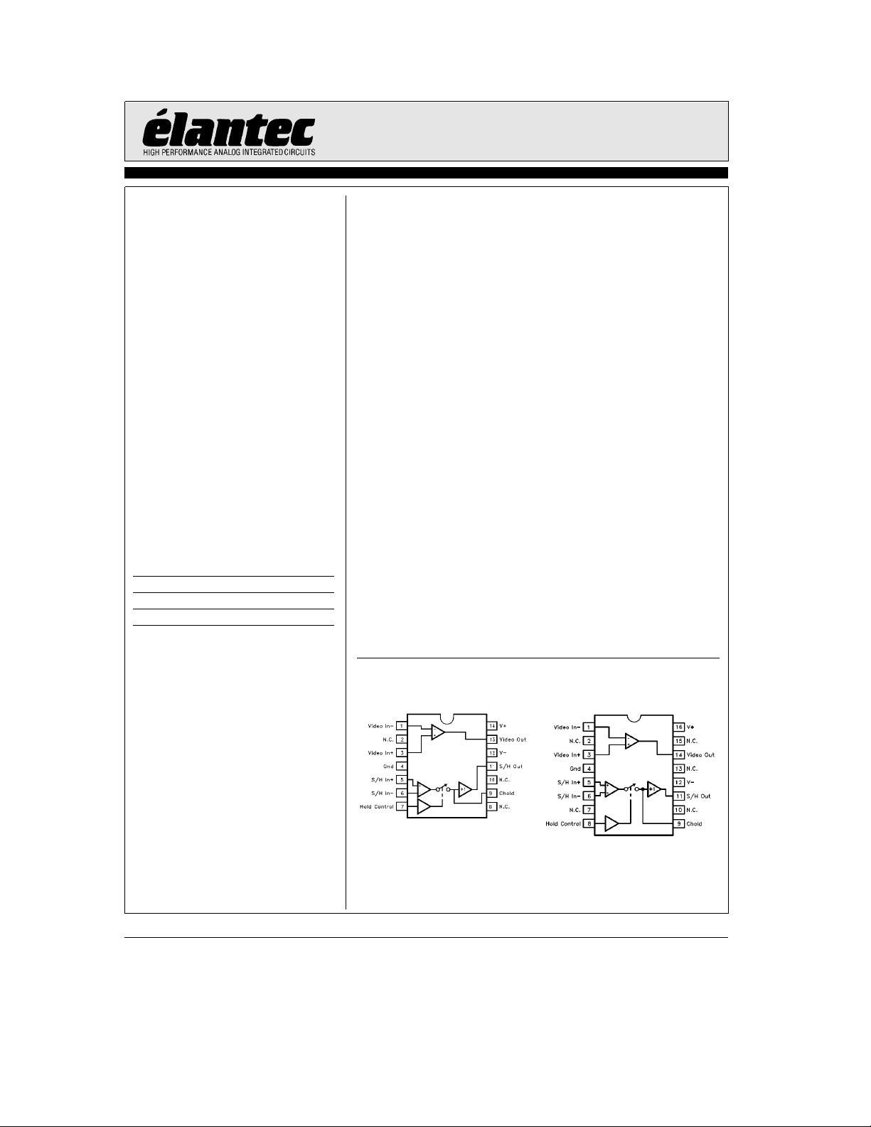
Connection Diagrams
14-Pin DIP Package 16-Pin SOL Package
2090– 1
2090– 2
Note: All information contained in this data sheet has been carefully checked and is believed to be accurate as of the date of publication; however, this data sheet cannot be a ‘‘controlled document’’. Current revisions, if any, to these
specifications are maintained at the factory and are available upon your request. We recommend checking the revision level before finalization of your design documentation. Patent pending.
©
1990 Elantec, Inc.
CMSÝ2090DS
Page 2
EL2090C
100 MHz DC-Restored Video Amplifier
Absolute Maximum Ratings
a
Voltage between V
Voltage between V
V
Current into V
Important Note:
All parameters having Min/Max specifications are guaranteed. The Test Level column indicates the specific device testing actually
performed during production and Quality inspection. Elantec performs most electrical tests using modern high-speed automatic test
equipment, specifically the LTX77 Series system. Unless otherwise noted, all tests are pulsed tests, therefore T
Test Level Test Procedure
,C
S/H
b
IN
HOLD
Current 60 mA
OUT
b
IN
I 100% production tested and QA sample tested per QA test plan QCX0002.
II 100% production tested at T
III QA sample tested per QA test plan QCX0002.
IV Parameter is guaranteed (but not tested) by Design and Characterization Data.
V Parameter is typical value at T
b
and V
, S/H
a
IN
, and GND pins (Va)a0.5V
,
a
IN
and HOLD Pins 5 mA
T
MAX
and T
MIN
A
per QA test plan QCX0002.
e
(T
25§C)
A
36V
Current S/H
Internal Power Dissipation See Curves
to (V
b)b
0.5V
Operating Ambient Temperature Range 0
Operating Junction Temperature
Plastic DIP or SOL 150
Storage Temperature Range
e
25§C and QA sample tested at T
e
25§C for information purposes only.
A
OUT
b
e
T
J
C
e
25§C,
A
16 mA
Cto75§C
§
65§Ctoa150§C
e
TA.
§
Open Loop DC Electrical Characteristics
e
g
V
S
Parameter Description Temp Min Typ Max Test Level Units
I
S
Video Amplifier Section (Not Restored)
V
OS
I
a
B
I
b
B
R
OL
A
VOL
V
O
I
SC
Sample-And-Hold Section
V
OS
I
B
I
OS
R
IN, DIFF
R
IN, COMM
V
CM
15V; R
L
e
150X,T
e
25§C unless otherwise specified
A
Total Supply Current Full 14 17 II mA
Input Offset Voltage Full 8 70 II mV
a
VINInput Bias Current Full 2 15 II mA
b
VINInput Bias Current Full 30 150 II mA
Transimpedance 25§C 300 V V/mA
Open-Loop Voltage Gain;
e
g
V
OUT
2V
Output Voltage Swing
e
g
V
S
e
g
V
S
15V; R
5V; R
e
2kX
L
e
150X
L
Full 56 65 II dB
Full
Full
g
g
3.0
g
12
13 II V
g
3.5 II V
Short-Circuit Current;
a
VINSet tog2V;bV
to Ground through 1 kX
IN
25§C
g
g
50
g
90
160 II mA
Input Offset Voltage Full 2 10 II mV
Input Bias Current Full 0.5 2.5 II mA
Input Offset Current Full 0.05 0.5 II mA
Input Differential Resistance 25§C 200 V kX
Input Common-Mode Resistance 25§C 100 V MX
Common-Mode Input Range Full
g
g
11
12.5 II V
C
TDis 3.9in
2
Page 3
EL2090C
100 MHz DC-Restored Video Amplifier
Open Loop DC Electrical Characteristics
e
g
V
S
Parameter Description Temp. Min Typ Max Test Level Units
Sample-And-Hold Section Ð Contd.
A
VOL
CMRR Common-Mode Rejection Ratio
PSRR Power-Supply Rejection Ratio
V
thresh
I
droop
I
charge
V
O
I
SC
Closed Loop AC Electrical Characteristics
e
g
V
S
Parameter Description Min Typ Max Test Level Units
Video Amplifier Section
SR SlewRate; V
BW Bandwidth;b3 dB 75 100 III MHz
Peaking
dG Differential Gain;
di Differential Phase;
Sample-And-Hold Section
BW Gain-Bandwidth Product 1.3 V MHz
DQ Sample to Hold Charge
DT Sample to Hold or Hold to
T
s
Note 1: The logic input is between 0V and 5V, with a 220X resistor in series with the HOLD pin and 39 pF capacitor from HOLD pin
15V; R
L
15V; C
L
to ground.
e
150X,T
e
25§C unless otherwise specified Ð Contd.
A
Large Signal Voltage Gain Full 15k 50k II V/V
V
V
CM
S
e
e
g
11V
g
5V tog15V
Full 75 95 II dB
Full 75 95 II dB
HOLD Pin Logic Threshold Full 0.8 1.4 2.0 II V
Hold Mode Droop Current Full 10 50 II nA
Charge Current Available to
Chold
Output Swing; R
e
2k Full
L
Short-Circuit Current 25§C
e
15 pF; C
(bVIN)e2.5 pF; R
stray
fromb2toa2V 600 V V/ms
OUT
g
1 dB 35 60 III MHz
g
0.1 dB 10 20 III MHz
F
Full
e
e
R
G
300X;R
g
g
g
L
90
10
10
e
g
135 II mA
g
13 II V
g
150X;C
17
hold
g
40 II mA
e
100 pF; T
e
25§C
A
VINfromb0.7V to 0.7V; 0.01 V %
e
F
3.58 MHz
V
fromb0.7V to 0.7V; 0.02 V
IN
Fe3.58 MHz
Injection (Note 1)
Sample Delay Time
Sample to Hold Settling
Time to 2 mV
1.5 5 III pC
20 V ns
200
V
§
ns
TDis 2.3inTDis 3.4in
3
Page 4
EL2090C
100 MHz DC-Restored Video Amplifier
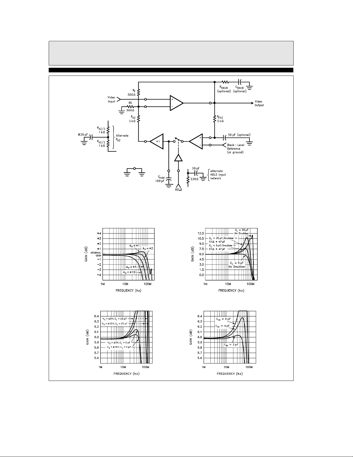
Figure 1. Typical Application (A
Typical Performance Curves
Relative Frequency Response
for Various Gains
Frequency Response Flatness
for Various Load
and Supply Conditions
ea
2)
V
Frequency Response with
Different Loads (A
Frequency Response Flatness vs
C
ea
,A
b
IN
V
ea
V
2
2090– 3
2)
2090– 4
2090– 5
4
Page 5

EL2090C
100 MHz DC-Restored Video Amplifier
Typical Performance Curves
Differential Gain and Phase vs
Supply Voltage; A
e
R
150X,VINfrom 0 toa0.7 V
L
Differential Gain vs DC Input
Offset; A
V
e
3.58 MHz, R
F
O
ea
ea
2,
V
2,
e
150X
L
Ð Contd.
DC
Deviation from Linear
Phase vs Frequency
Differential Phase vs DC Input
Offset; A
F
e
O
ea
V
3.58 MHz, R
2,
e
150X
L
Differential Gain vs DC Input Offset;
ea
A
2 and F
V
e
O
30 MHz, R
e
L
150X
2090– 12
Differential Phase vs DC Input Offset;
ea
A
V
2, F
e
O
30 MHz, R
e
150X
L
2090– 6
5
Page 6

EL2090C
100 MHz DC-Restored Video Amplifier
Typical Performance Curves
Sample-to-Hold Change
Injection vs Temperature
Ð Contd.
S/H Available Charge Current
vs Temperature
2090– 7
Typical Droop Current vs
Temperature, V
e
g
15V
S
Supply Current vs
Supply Voltage
Supply Current vs Temperature;
e
g
V
15V
S
2090– 8
2090– 9
6
Page 7

EL2090C
100 MHz DC-Restored Video Amplifier
Typical Performance Curves
Maximum Power Dissipation
vs Ambient TemperatureÐ
14-Pin PDIP and 16-Pin SOL
Ð Contd.
2090– 10
Applications Information
The EL2090C is a general purpose component
and thus the video amplifier and sample-andhold pins are uncommitted. Therefore much of
the ultimate performance as a DC-restored video
amplifier will be set by external component values and parasitics. Some application considerations will be offered here.
The DC feedback from the sample-and-hold can
be applied to either positive or negative inputs of
the video amplifier (with appropriate phasing of
the sample-and-hold amplifier inputs). We will
consider feedback to the inverting video input.
During a sample mode (the HOLD input at a logic low), the sample-and-hold acts as a simple nulling op-amp.
Ideally, the DC feedback resistor Raz is a high
value so as not to couple a large amount of the
AC signal on the video input back to the sampleand-hold amplifier output. The sample-and-hold
output is a low impedance at high frequencies,
but variations of the DC operating point will
change the output impedance somewhat. No
more than a few ohms output impedance change
will occur, but this can cause gain variations in
the 0.01% realm. This DC-dependent gain
change is in fact a differential gain effect. Some
small differential phase error will also be added.
The best approach is to maximize the DC feedback resistor value so as to isolate the sampleand-hold from the video path as much as possible. Values of 1 kX or above for Raz will cause
little to no video degradation.
This suggests that the largest applicable power
supply voltages be used so that the output swing
of the sample-and-hold can still correct for the
variations of DC offset in the video input with
large values of Raz. The typical application circuit shown will allow correction of
g
1V inputs
with good isolation of the sample-and-hold output. Good isolation is defined as no video degradation due to the insertion of the sample-andhold loop. Lower supply voltages will require a
smaller value of DC feedback resistor to retain
correction of the full input DC variation. The
EL2090 differential phase performance is optimum at
g
9V supplies, and differential gain only
marginally improves above this voltage. Since all
video characteristics mildly degrade with increasing die temperature, the
what better than
g
15V supplies are quite usable.
g
g
9V levels are some-
15V supplies. However,
Ultimate video performance, especially in HDTV
applications, can also be optimized by setting the
black-level reference such that the signal span at
the video amplifier’s output is set to its optimum
range. For instance, setting the span to
output is preferable to a span of 0V to
g
a
2V. The
1V of
curves of differential gain and phase versus input
DC offset will serve as guides.
The DC feedback resistor may be split so that a
bypass capacitor is added to reduce the initially
small sample-and-hold transients to even smaller
levels. The corruption can be reduced to as low as
1 mV peak seen at the video amplifier output.
The size of the capacitor should not be so large as
to de-stabilize the sample-and-hold feedback
loop, nor so small as to reduce the video amplifier’s gain flatness. A resistor or some other video
isolation network should be inserted between the
video amplifier output and the sample-and-hold
input to prevent excessive video from bleeding
through the autozero section, as well as preventing spurious DC correction due to video signals
confusing the sample-and-hold during autozero
events. Figure 1 shows convenient component
values. A full 3.58 MHz trap is not necessary for
suppressing NTSC chroma burst interaction with
the sample-and-hold input; the simple R-C network suggested in Figure 1 suffices.
7
Page 8

EL2090C
100 MHz DC-Restored Video Amplifier
Applications Information
The HOLD input to the sample-and-hold has a
1.4V threshold and is clamped to a diode below
ground and 6V above ground. The hold step characteristics are not sensitive to logic high nor low
levels (within TTL or CMOS swings), but logic
slewrates greater than 1000V/ms can couple noise
and hold step into the sample-to-hold output
waveforms. The logic slewrate should be greater
than 50V/ms to avoid hold jitter. To avoid artificially high droop in hold mode, the Chold pin
and Chold itself should be guarded with circuit
board traces connected to the output of the sample-and-hold. Low-leakage hold capacitors should
be used, such as mica or mylar, but not ceramic.
The excellent properties of more expensive polystyrene, polypropylene, or teflon capacitors are
not needed.
The user should be aware of a combination of
conditions that may make the EL2090 operate incorrectly upon power-up. The fault condition can
be described by noticing that the sample-andhold output (pin 11) appears locked at a voltage
close to V
less of changes at the inputs to the sample-andhold (pins 5 and 6) or to the HOLD control input
(pin 7). Two conditions must occur to bring this
about:
1. A large value of CholdÐusually values of
1000 pF or more. This is not an unusual situation. Many users want to reduce the size of the
. This voltage is maintained regard-
CC
Ð Contd.
hold step and increasing Chold is the most direct way to do this. Increasing Chold also reduces the slew rate of the sample and hold section but because of the limited size of the video signal, this is usually not a limitation.
2. A sampling interval (dictated by the HOLD
pin) that is too small. By small, we mean less
than 2 ms.
For a sampling interval that is wide enough,
there is enough time for the loop to close and for
the amplifier to discharge whatever charge was
dumped onto Chold it during the initial power
spike and to then ramp up (or down) to the voltage that is proper for a balanced loop. When the
sampling interval is too small, there is insufficient time for internal devices to recover from
their initial saturated state from power-up because the feedback is not closed long enough.
Therefore, typical recovery times for the loop are
2 ms or greater. Summarizing, the two things
that could prevent proper saturation recovery are
(as mentioned above) too large a capacitor which
slows the charge and discharge rate of the stored
voltage at Chold and too small a sampling interval in which the entire feedback loop is closed.
The circuit shown below prevents the fault condition from occurring by preventing the node from
ever saturating. By clamping the value of Chold
to some value lower than the supply voltage less
2090– 13
8
Page 9

EL2090C
100 MHz DC-Restored Video Amplifier
Applications Information
a saturation voltage, we prevent this node from
approaching the positive rail. The maximum
voltage is set by the resistive voltage divider (between V
This value can be adjusted if the maximum size
of the input signal is known. The diode used is an
off-the-shelf 1N914 or 1N916.
As is true of all 100 MHz amplifiers, good bypassing of the supplies to ground is mandatory.
1 mF tantalums are sufficient, and 0.01 mF leaded
chip capacitors in parallel with medium value
electrolytics are also good. Leads longer than (/2
can induce a characteristic 150 MHz resonance
and ringing.
The V
absolute minimum of parasitic capacitance. Stray
capacitance of more than 3 pF will cause peaking
and compromise the gain flatness. The bandwidth of the amplifier is fundamentally set by
the value of Rf. As demonstrated by the frequen-
a
and GND) R1 and R2 plus a diode.
of the video amplifier should have the
b
IN
Ð Contd.
cy response versus gain graph, the peaking and
bandwidth is a weak function of gain. The
EL2090 was designed for Rf
mum gain flatness at Av
sponse is flattest for Rf
e
use Rf
is accentuated by load capacitance or
pacitance the value of Rf will have to be increased, and some bandwidth will be sacrificed.
The V
into an inductive source impedance. If the source
is physically remote and a terminated input line
is not provided, it may be necessary to connect
an input ‘‘snubber’’ to ground. A snubber is a resistor in series with a capacitor which de-Q’s the
input resonance. Typical values are 100X and
30 pF.
The output of the video amplifier is sensitive to
capacitive loads greater than 25 pF, and a snubber to ground or a resistor in series with the output is useful to isolate reactive loads.
270X. In situations where the peaking
of the video amplifier should not look
a
IN
e
300X giving opti-
ea
e
2. Unity-gain re-
360X; gains ofa5 can
b
input ca-
9
Page 10

EL2090C
100 MHz DC-Restored Video Amplifier
EL2090 Macromodel
* Revision A, October 1992
.param vclamp
*
* Connections: Vidin
*
*
*
*
*
*
*
*
*
*
.subckt EL2090/EL 3 1 14 12 13 5 6 11 7 9
**
******** Video Amplifier ******************* ************ Sample & Hold *************************
**
e1200301.0 g40490561e-3
vis 20 34 0V vcur 49 42 0v
h2 34 38 vxx 1.0 r43 6 0 100Meg
r10 1 36 25 r44 5 0 100Meg
l1 36 38 20nH r40 42 0 4K
iinp3010mA d41 50 42 diode
iinm105mA d42 42 51 diode
h1 21 0 vis 600 v41 50 0
r2 21 22 1K v42 0 51Àvclamp
d1 22 0 dclamp g41 44 0 42 0 200e-6
d2 0 22 dclamp r42 44 0 31Meg
e2 23 0 22 0 0.00166666666 d45 9 14 diode
l5 23 24 0.7mH d46 12 9 diode
c5 24 0 0.5pF s1 44 9 48 0 swa
r5240600 e40460900.95
g1 0 25 24 0 1.0 i40 0 9 10nA
rol 25 0 400K r45 46 47 70
cdp 25 0 7.7pF l40 47 11 70nH
q1 12 25 26 qp c40 7 9 0.32pF
q2 14 25 27 qn r47 7 48 10K
q3 14 26 28 qn c41 48 0 3pF
q4 12 27 29 qp *
r7 28 13 4 * Models
r8 29 13 4 *
ios1 14 26 2.5mA .model qn npn(is
ios2 27 12 2.5mA .model qp pnp(is
ips 14 12 7.2mA .model dclamp d(is
ivos 0 33 5mA .model diode d
vxx 33 0 0V .model swa vswitch(von
r11 33 0 1K .ends
eÀb
0.002 * (TEMPb25)
a
Vidin
l
ll
lll
lll l
lll l l
lll l l l
lll l l l l
lll l l l l l
b
a
Vsupply
Ó
b
Vsupply
Vid Out
S/H In
a
S/H In
b
S/H Out
Hold Control
lll l l l l l l
lll l l l l l l l
À
Ó
vclamp
Ó
e
5e-15 bfe500 tfe0.1nS)
e
5e-15 bfe500 tfe0.1nS)
e
1e-30 ibve0.02 bve2.75 ne4)
e
1.2v voffe1.6v roffe1e12 rone100)
Chold
TDis 6.6in
10
Page 11

EL2090C
100 MHz DC-Restored Video Amplifier
EL2090 Macromodel
Ð Contd.
2090– 15
Sample and Hold Amplifier
11
Page 12

EL2090C
100 MHz DC-Restored Video Amplifier
EL2090CJanuary 1996 Rev D
EL2090 Macromodel
Ð Contd.
2090– 14
Video Amplifier
General Disclaimer
Specifications contained in this data sheet are in effect as of the publication date shown. Elantec, Inc. reserves the right to make changes
in the circuitry or specifications contained herein at any time without notice. Elantec, Inc. assumes no responsibility for the use of any
circuits described herein and makes no representations that they are free from patent infringement.
WARNING Ð Life Support Policy
Elantec, Inc. products are not authorized for and should not be
used within Life Support Systems without the specific written
consent of Elantec, Inc. Life Support systems are equipment in-
Elantec, Inc.
1996 Tarob Court
Milpitas, CA 95035
Telephone: (408) 945-1323
(800) 333-6314
Fax: (408) 945-9305
European Office: 44-71-482-4596
tended to support or sustain life and whose failure to perform
when properly used in accordance with instructions provided can
be reasonably expected to result in significant personal injury or
death. Users contemplating application of Elantec, Inc. products
in Life Support Systems are requested to contact Elantec, Inc.
factory headquarters to establish suitable terms & conditions for
these applications. Elantec, Inc.’s warranty is limited to replacement of defective components and does not cover injury to persons or property or other consequential damages.
Printed in U.S.A.12
 Loading...